Article

Ultraviolet Laser Sintering of Printed Nickel Oxide Nanoparticles for Thin-Film Thermistor via Aerosol Jet Printing Technology

1
Department of Mechanical Engineering, National Taiwan University, No. 1, Section 4, Roosevelt Road, Taipei 10617, Taiwan
2
Taiwan Instrument Research Institute (TIRI), National Applied Research Laboratories (NARLabs), No. 20, R&D Road VI, Hsinchu Science Park, Hsinchu City 30076, Taiwan
*
Authors to whom correspondence should be addressed.
Appl. Sci. 2022, 12(14), 7206; https://doi.org/10.3390/app12147206
Submission received: 23 June 2022 / Revised: 11 July 2022 / Accepted: 15 July 2022 / Published: 17 July 2022

Abstract

:
In this study, nickel oxide (NiO) thin films were printed by an aerosol jet printer, which is capable of fabricating thin films on the curve substrate via air stream. To approach high efficiency fabricating thin film thermistors in small batch sizes, the printed NiO nanoparticle thin films were sintered by using a 355 nm wavelength ultraviolet (UV) laser; this novel fabrication method reduced several steps of the conventional manufacturing process of the thermistor. Compared with furnace heat treatments of the NiO thermistor in previous studies, the UV laser sintering not only significantly improved the electrical properties but decreased the treatment time from an hour to a second. Since the resistance declined, the thermistor has been operated at an ambient temperature, which provides ready measurement. The resistance and morphology of the thin films were analyzed for evaluating the effect of the laser treatment. To identify the proper UV laser parameters, three laser parameters, including laser output energy, frequency, and scanning speed, were studied. Due to the laser-sintering parameters, namely, 2 W, 150 mm/s, 90 kHz, and a B value of 4683 K, the resistance has been reduced from 106.8 MΩ to 6.15 MΩ at 100 °C. The experiments exhibited a series of analyses for sintering states and defects of printed NiO nanoparticle thin film, which were sintered by UV laser. For NiO nanoparticles, UV laser has higher absorption energy than that of other wavelength lasers, when excess laser output was applied to the NiO thin film, cracks were observed on the surface. It was found that the crystal plane distances were not affected by recrystallization, but the cracks were based on the XRD analysis. Based on the analysis, there were obvious regional compressive stains before the appearance of cracks, and the uneven shrinking strains caused the cracks on the surface as energy irradiation increased.

1. Introduction

Temperature sensors are widely used in research and industrial applications, such as IC (integrated circuit) chip, micro-resistance temperature detector array [1], and metal cutting [2]. There are four types of commercial temperature sensors: thermocouple, thermistor, resistance temperature detector (RTD), and IC sensor [3]. The thermistor is the only sensor that can be printed as a thin film. NiO is a readily obtained material that is low in toxicity. NiO nanoparticles can be synthesized through several processes, such as the sol–gel and electric arc discharge methods [4,5]; therefore, over the past few decades, NiO has been frequently used in research concerning gas sensors [6,7,8], lactate sensors [9], P-type semiconducting materials [10], supercapacitors [11,12], catalysts [13], electrodes of battery [14], and resistive switching memories [15].
Additive manufacturing (AM) has been extensively studied [16,17]; Khorasani et al. [18] indicated that additive manufacturing (AM) prevented expensive tool-making procedures and increased the efficiency of the manufacturing process. For the thin film fabrication techniques of AM, such as aerosol jet and inkjet, these two printing methods have been applied for printing NiO thermistors in previous studies. NiO is sensitive to temperature variation, which makes it a suitable material for fabricating thermistors. Huang et al. [19] used inkjet to fabricate nickel oxide (NiO) nanoparticle thermistors on flexible substrates. The printed NiO thermistors exhibited good reliability when they were bent, making them suitable temperature sensors for devices with curved surfaces. Wang et al. [20] used aerosol jet printing to print NiO thermistors on three types of turning inserts with different geometric surfaces and successfully achieved high accuracy of measurement of cutting temperatures. The heat treatment of NiO thin films is frequently executed in a furnace [3,4]. Furnace calcining is a common method for the annealing or sintering of printed thin films [6,7,8,9,11,12,13,14,15,16,17,18,19,20,21]. However, thermal treatment in a furnace is typically time-consuming and can last for several hours [21]. If there are only a few NiO thin film sensors to be heat-treated at a time, it is not economical. Furthermore, there was a phenomenon called necking [22,23]. It appeared while the energy of sintering or calcination was too large, the adjacent nanoparticles merged into big particles, and the original position of nanoparticles became holes or defects. Therefore, this study analyzed the morphology and strain of UV laser-sintered NiO thin films.
Therefore, to improve the efficiency of manufacturing NiO thermistors, laser treatment was used in sintering or annealing NiO thin film sensors. Kemary et al. [24] established the optical absorption spectra of NiO nanoparticles, the strongest absorption wavelength of which was approximately 329.5 nm (~3.75 eV), and it was within the UV region (200–400 nm). Based on the research results, this study investigated how UV laser treatment was applied in converting thin films into functional thermistors. Lee et al. applied a continuous wave (wavelength: 514.5 nm) laser to fabricate Ni electrodes by sintering NiO nanoparticle thin films. Through a photothermal reaction of NiO, the agents in the solvent were reduced and the results demonstrated that the Ni thin films had high electrical conductivity and transmittance [25]. Paeng et al. modulated the power density and illumination time of the 514.5 nm continuous-wave laser. To analyze the sintering state and mechanism of the photo-physical reductive process of Ni, the study estimated the temporal evolution of transmittance, reflectance, and electrical conductance to establish a diagnostic process as four states: oxidation, reduction, sintering, and reoxidation [22]. In the aforementioned studies about making Ni thin films [22,25], a 514.5 nm laser was applied to form a conducting Ni thin film, while a stronger energy absorption wavelength, a 355 nm laser, was used in this study to improve the electrical properties of NiO by advancing the connection of nanoparticles without reductive sintering.
To achieve a repeatable and stable manufacturing process of the thermistor, this study focused on the optimization of ultraviolet (UV) laser-sintering parameters, which provided better electrical properties and manufacturing efficiency. Thus, after the fabrication of NiO thin films and UV laser sintering, the electrical properties of sintered thin films were measured by multimeter at two different temperatures for resistance performance and sensitivity calculation. Each laser parameter setting was executed three times for the estimation of stability and repeatability, which was exhibited by error bars. The shorter error bars indicated low deviation of experimental replications, while the longer ones represented high deviation. For the effect analyses of UV laser sintering on NiO, the morphology performances and Williamson–Hall plots from XRD patterns were applied to illustrate the sintering states and mechanism of cracks on the sintered thin films.
The resistances and sensitivity of NiO thin film sensors were studied for understanding the effects of UV laser on NiO thin films. Through finding an NiO thin film with low resistance and high sensitivity, the optimal laser treatment setting was obtained within the decided range of the laser parameters.

2. Method

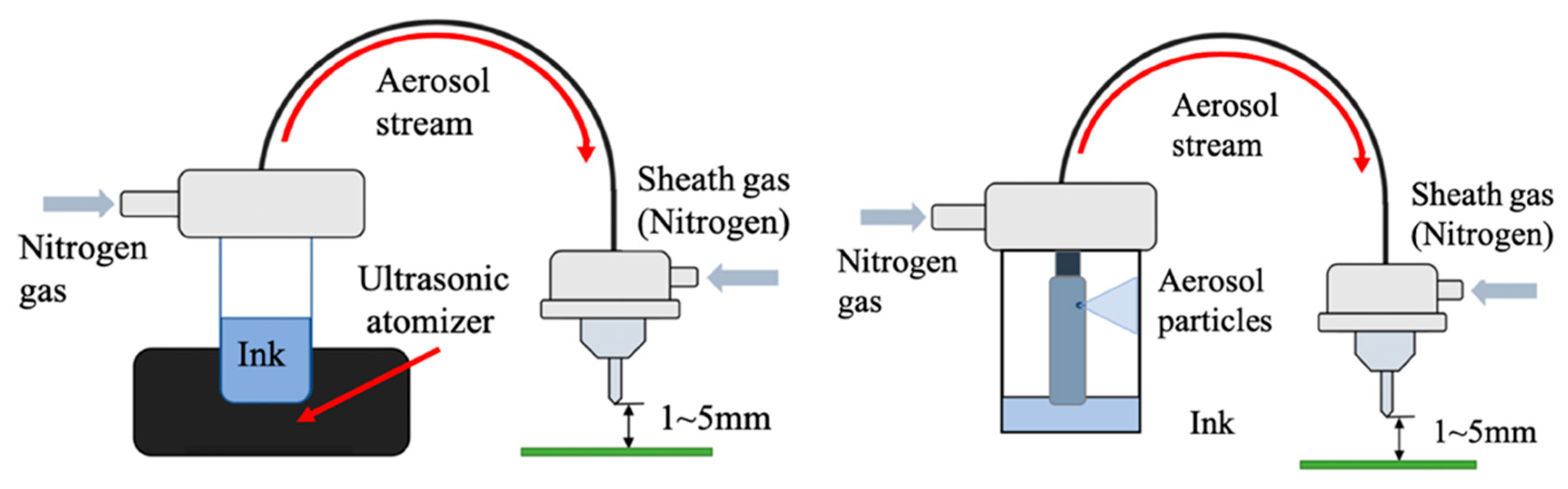
2.1. NiO Ink Preparation and Fabrication Process of Thin Film

For NiO nanoparticle ink preparation, the ink formula consisted of 0.5 g of NiO nanoparticles (Sigma-Aldrich, Burlington, MA, USA), 8 g of deionized water, and 2 g of propylene glycol methyl ether. The ink formula was referred to that of Huang et al. [19]. However, the particle size distribution was altered for the aerosol jet printer (AJP) with an average particle size of < 50 nm. NiO nanoparticles are insoluble in water, and the pH value of the recipe was adjusted to avoid particle aggregation and precipitation, achieving a stable suspension of nanoparticles. In a previous study [20], the suggested pH value for AJP ink was 3 to 5.
An AJP with a nozzle diameter of 150 μm (Optomec, Albuquerque, NM, USA) was used to print NiO nanoparticle thin films in this study. An AJP features an atomizer that turns ink into small droplets; then, N2 pressure transfers the droplets to the nozzle, and the nitrogen flow is used to focus the aerosol stream by controlling the width of the print track [26].The AJP used in this study has two atomizer modules, namely, an ultrasonic atomizer (Figure 1 left) and a pneumatic atomizer (Figure 1 right). Viscosity is the main determinant of which module should be employed. An ultrasonic atomizer is only capable of operating with low viscosity (1–10 cP), whereas a pneumatic atomizer is made for high-viscosity ink (1–2500 cP); the ultrasonic atomizer module was applied in this study. An AJP can operate on curved surfaces, the printed ink tracks can be formed without aligning the nozzle on the substrate; aerosol jet printing differs starkly from conventional printing techniques.
For the detailed information of printing process, the width of printing the NiO track was 30 μm, the printing speed was 2 mm/s, and the spacing of tracks was 20 μm; therefore, the overlap of the tracks was 10 μm, which produced even NiO thin films. In Table 1, the detailed information of the raw NiO thin films was exhibited.
The substrates used for printing NiO thin films were commercial flat glasses with indium tin oxide (ITO) interdigital electrodes that were designed for resistance signal detection, as shown in Figure 2b. In Figure 2a, the printed NiO thin films are shown by 4 mm2 gray dashed square. These ITO interdigital electrodes were open circuit, and thus the resistance signal can only be detected after sintered NiO thin films were fabricated on the electrodes. In our previous study [21], NiO thin films were fabricated over the silver electrodes and the substrates were thermal resistant tape, Kapton® (DuPontTM, Inc., Wilmington, DE, USA). The study found that the thermal resistant tape could be deformed under 80% UV LED light irradiation. Furthermore, in Figure 3b, height differences were clearly visible on the surface. In this color map, the red color indicated the highest spot, while blue represented lowest spot. According to the result, the thickness of NiO thin films was only 15 microns thick, yet the sliver electrodes were approximately 15~17 microns. The overlap of NiO and sliver caused a significant height difference, which might have affected the results of UV laser sintering. Therefore, the commercial ITO glass substrates were applied to eliminate the factor of height difference and substrate deformation in this study (see Figure 3a).
Furthermore, some satellite points were found in the printed raw NiO thin films. The results of the height analysis from confocal microscopy showed the height of satellite points were 1 to 5 μm. Compared with silver electrodes, the satellite points did not cause significant uneven surface.

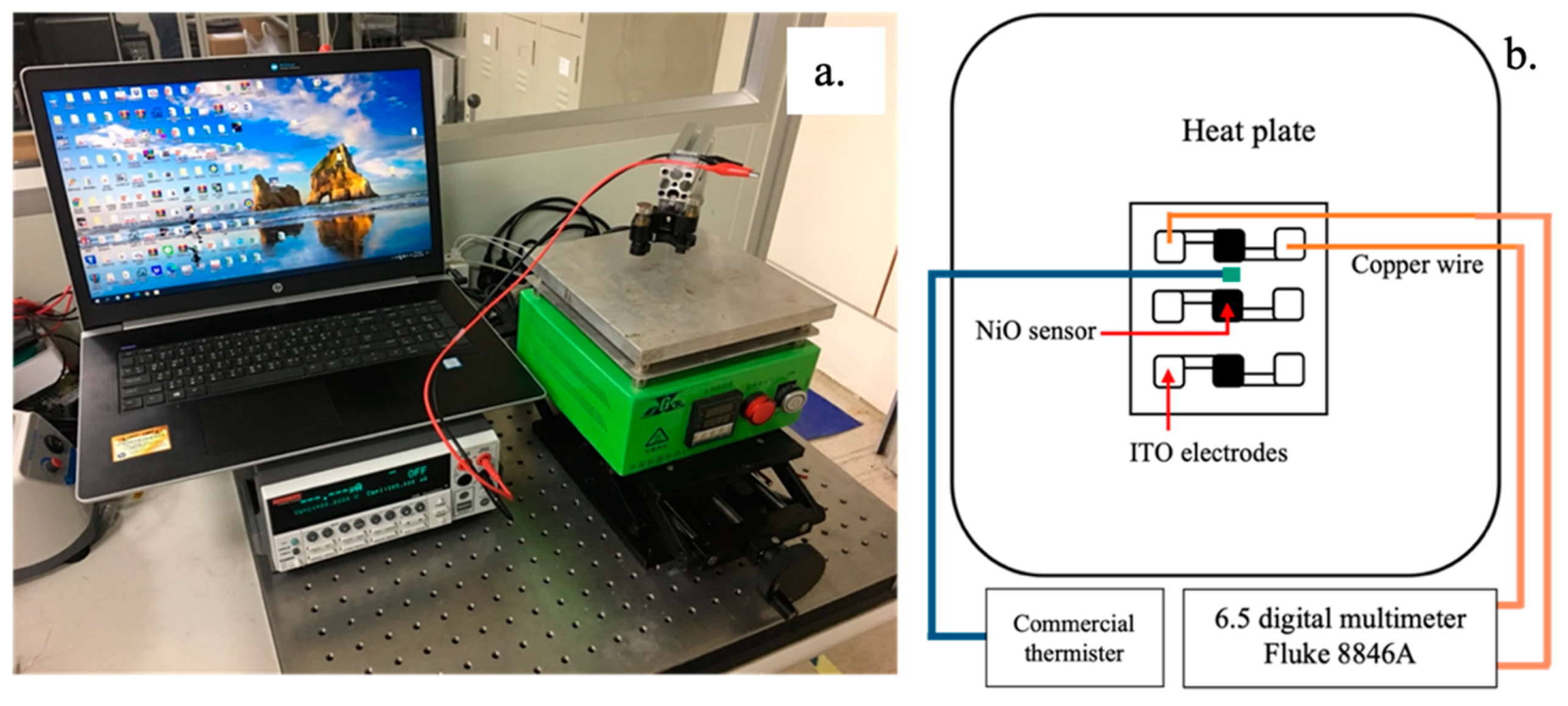
2.2. Experimental Design

The galvo scanning system of the UV laser device included a two-axis XY scanner (Raylase AG model SS-15) with a Nd:YVO4 solid-state Q-switched UV laser source (AVIA 355-14; Coherent Inc., Santa Clara, CA, USA) that emits a 355 nm wavelength and whose focal length is 110 mm. The laser parameters of interest in the experiments were laser power output, frequency, and scanning speed. The working distance was 150 mm, which used a defocused laser beam. The scanning speeds were 100 mm/s, 125 mm/s, and 150 mm/s. Laser power output of 1 W, 1.5 W, 2 W, 2.5 W, and 3 W were used for prior experiments, which were done for selecting the range of laser power output with 100 mm/s and 90 k Hz. The results showed the 3 W power output was too powerful and thus impaired the integrity of the printed NiO thin films. The cracks and flakes on the surface caused an open circuit (see Figure 4b). On the contrary, the 1 W laser output had an inefficient effect on sintering NiO nanoparticles in a laser scanning speed 100 mm/s (Figure 4a); thus, thin films remained insulated. The characteristic of these thin films was similar to the electrical property of the furnace-curried NiO thin films at ambient temperature, where the resistances were too high to be measured [21]. Therefore, the laser power outputs were determined to be 1.5 W, 2 W, and 2.5 W. The laser settings are summarized in Table 2, and each setting was executed three times for experimental replications and statistical difference (p value). The rest of the parameters of the laser system remained the same.
In order to define the optimal parameters setting from the experiments, the optimized condition was determined as the lowest resistance with the lowest error bar since the short error bar represents low deviation in the same laser parameters setting. Besides electrical analysis, the other characterization analyses of sintered NiO thin films were studied, including the morphology form SEM and confocal microscopy, the XRD pattern for sintering states and defect analyses, these analyses are introduced and further illustrated in the next section.

2.3. Characterization of NiO Thin Films

The sensitivity of the thermistor is generally presented as a B value. For a commercial thermistor, the B value must exceed 3500 K [27], which ensures the thermistor has adequate sensitivity. The B value is calculated using the Arrhenius equation [19,27]:
B = ln ( R 1 ) ln ( R 2 ) 1 T 1 1 T 2
where resistances R1 and R2 are measured at temperatures T1 and T2, respectively (temperature unit: Kelvin). T1 is the initial temperature, and T2 is the final temperature. These two temperatures were set at 35 °C and 100 °C in this study. The samples were heated on a heat plate (Figure 5), and a commercial thermistor was placed alongside the glass substrates to monitor temperature variation. For the resistance measurement, a Fluke 8846A 6.5 digital multimeter (Fluke Corporation, Everett, Washington, DC, USA; Figure 5a) was used to detect the resistance in a steady state. Single-factor analysis of variance was conducted to identify statistical differences between laser parameters (significance level set at p < 0.05) [28].
A confocal microscopy (Keysight VK-X200, Keyence Corporation, Osaka, Japan) and a scanning electron microscope (SEM) (S-4800, Hitachi, Japan Tokyo) were applied to investigate the surface of the objects. In addition, XRD patterns were used to measure the crystal plane distance and strain of the NiO thin films. The crystal plane distances were acquired by Scherrer equation
D = kλ/βcosθ
D is the crystal plane distance, λ is the wavelength of the X-ray, k is the shape factor, β is the full width at half maximum of characteristic peaks, and θ is the angle of incidence (Bragg angle); as the XRD pattern is applied, the strain ( ε ) of the NiO thin films is calculated using the Williamson–Hall equation:
β cos θ = k λ D + 4 ε sin θ
where k is the shape factor, λ is the X-ray wavelength, θ is the Bragg angle, and D is the crystal plane distance that can be acquired by Bragg’s law:
2 D   sin θ = n λ
Therefore, the micro-strain ε could be estimated from the slope of the linear regression of the Williamson–Hall plots ( β cos θ versus 4 sin θ ).

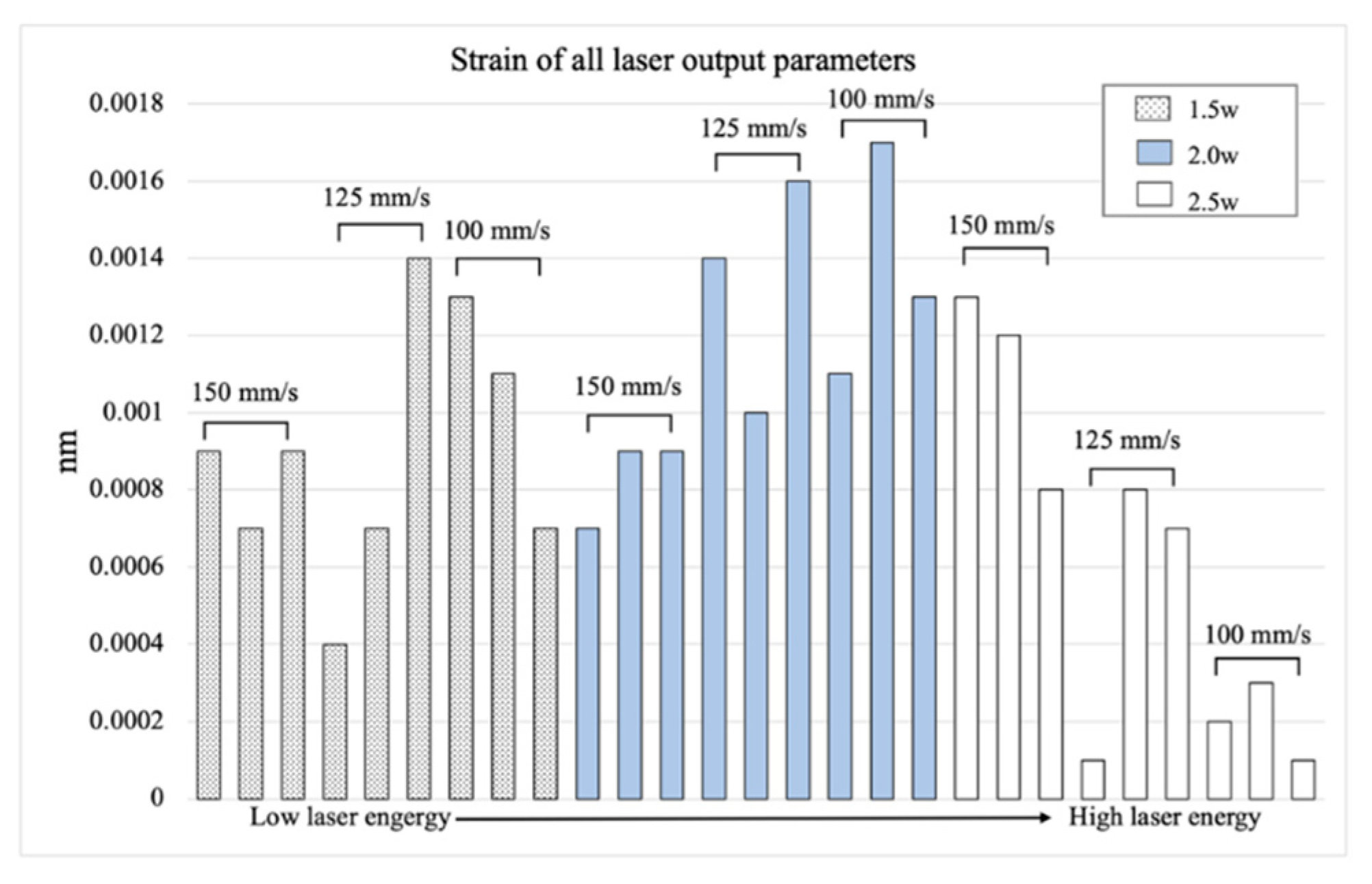
3. Results and Discussion

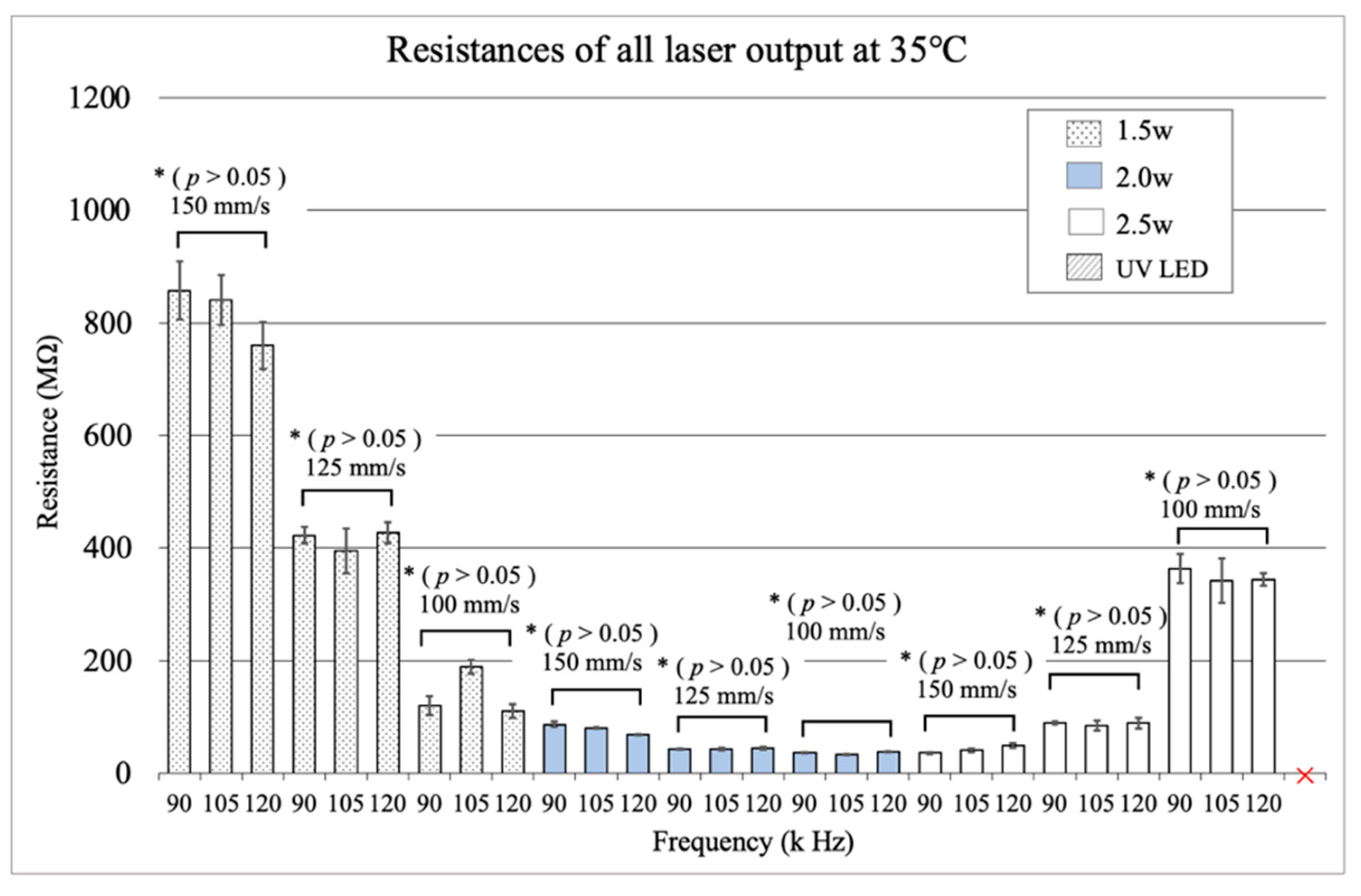
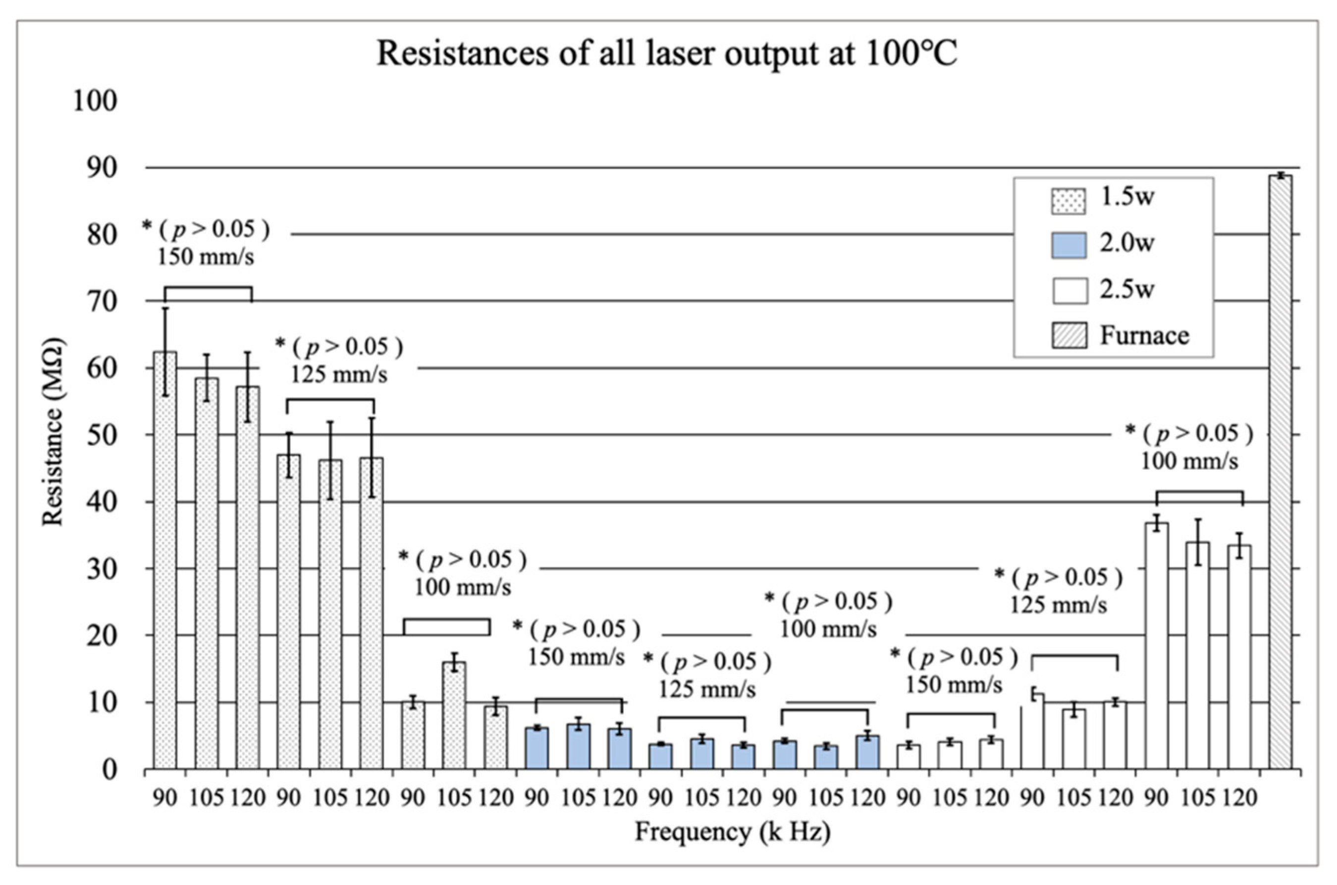
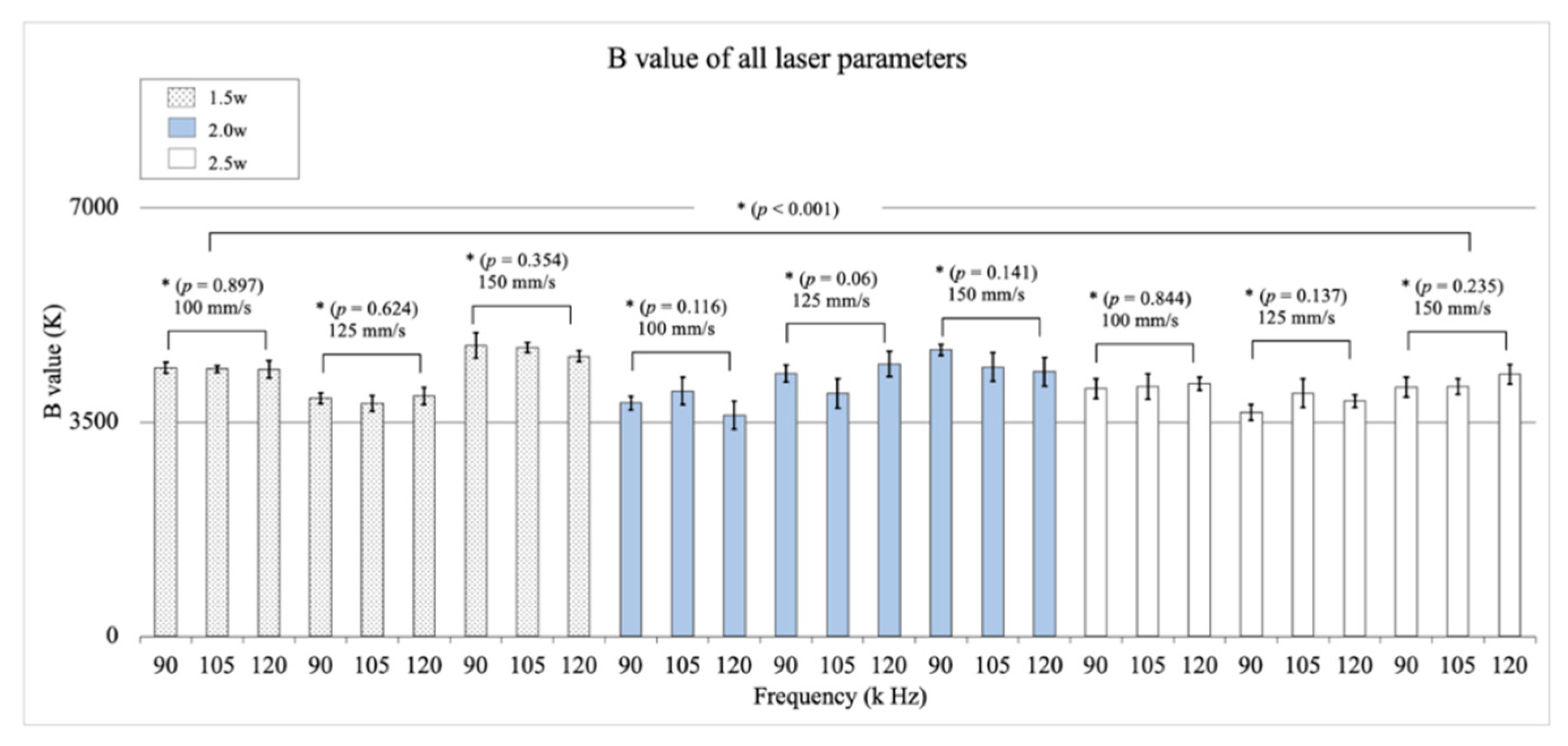
3.1. Resistance Experiments

Our previous study [21] showed that NiO thin film sensors cured in a furnace have extremely high resistance and can thus be considered insulators at atmospheric temperature. Therefore, the resistances of furnace-cured and UV laser-sintered NiO sensors were compared in this study. Figure 6 and Figure 7 present the resistance of laser-sintered NiO thin films that were measured at 35 °C and 100 °C, respectively; the sintered NiO thin film showed better sensitivity in the range of 35 °C to 100 °C.
In Figure 6, the 1.5 W laser output with the low scanning speed resulted in low resistance. The resistance dramatically declined while increasing laser energy (lower scanning speed). It exhibited the adjacent nanoparticles rapidly and massively joined together. Therefore, slowing down the scanning speed or delivering more energy on the thin films efficiently reduced the resistance of the NiO thin film sensors. Additionally, the error bars of experimental replications were much larger than those of the NiO thin films sintered at other laser powers, which means the manufacturing process was not stable under the scanning speeds of 100 mm/s to 150 mm/s, the frequencies of 90 k to 120 k Hz, while the energy output was set at 1.5 W. Compared with parameters with 2W laser output, the NiO thin films was not fully sintered by 1.5 W laser output with any scanning speed or frequency.
In the 2 W laser output experiments (blue bar chart), as scanning speed increased, the decrease of resistances tendency was slowed and the energy absorption of NiO thin films approached the saturation state. The variations of experimental replications of NiO thin film resistance decreased significantly; it is inferred that 2 W laser output with a scanning speed of 100 mm/s to 150 mm/s weas the adequate energy for the stable sintering process. The variations of experimental replications of parameters with 2.5 W laser output were also small; however, the trend of resistances increased while the scanning speed accelerated. The excess energy absorption resulted in diminished electrical performance. This phenomenon was also observed in previous research [22,23].
Regarding the effect of the laser frequency setting, the variation of frequency did not affect any trend of resistances in Figure 6 and Figure 7. Thus, a single-factor analysis of variance (ANOVA) was performed to evaluate the statistical difference of frequency variation (p value < 0.05). The conditions of single-factor analysis were fixed laser outputs and fixed scanning speeds; frequency was the only varied factor. Figure 6 and Figure 7 show the p values of laser frequency settings (90 k to 120 k Hz) with identical laser output and speed; the result indicated all p values of frequencies were above 0.05, which means the influence of frequency variation on the resistance performance was insignificant in this study.
The equation of laser pulse overlapping rate explained why the frequency variation did not affect the results—laser pulse overlapping rate directly affects the energy adsorption. The higher overlapping rate causes higher irradiation energy per area, while the lower overlapping rate represents lower energy absorption. The laser pulse overlapping rate equation can be defined as (Equation (5)) [29]:
R overlapping = ( 1 v D × f )   100 %
where D is the spot size (mm), ν is the scanning speed (mm/s), and f is the frequency (pulse repetition rate) in Hz (1/s). The distance between the focal lens and workpiece was fixed at 150 mm; thus, the laser spot size (D) was identical in each experiment. For the same scanning speed, the only factor that affects the overlapping rate is frequency in Equation (5). The maximum frequency variation was 30 k Hz (90 k Hz to 120 k Hz) in the experiments, which caused the similar overlapping rates. Taking D as 0.1 mm and ν as 100 mm/s, the calculated laser pulse overlapping rates of 90 k, 105 k, and 120 k Hz were 98.9%, 99%, and 99.1%, respectively.
In Figure 8, the sensitivity results had no tendency within the entire range of the laser parameters. Since the tendency of resistance variations at 35 °C and 100 °C were similar, the sensitivities did not show an obvious difference. All sensitivities (B values), however, meet the minimum requirement (B value: 3500 K) of commercial negative temperature coefficient (NTC) thermistors [19]. According to the above experimental results, the optimal laser parameters were determined to be 2 W, 150 mm/s, and 90 kHz, and the corresponding B value was 4683 K.

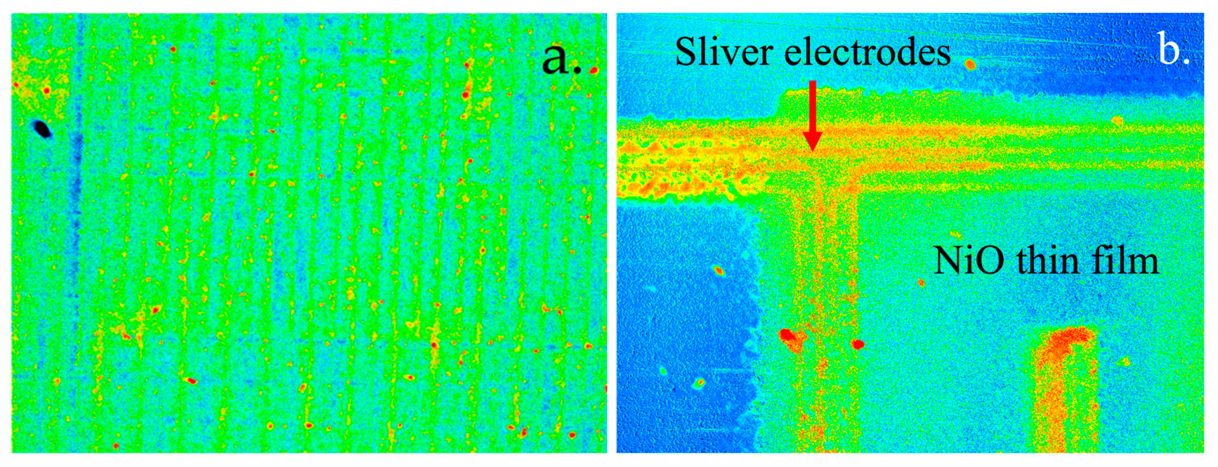
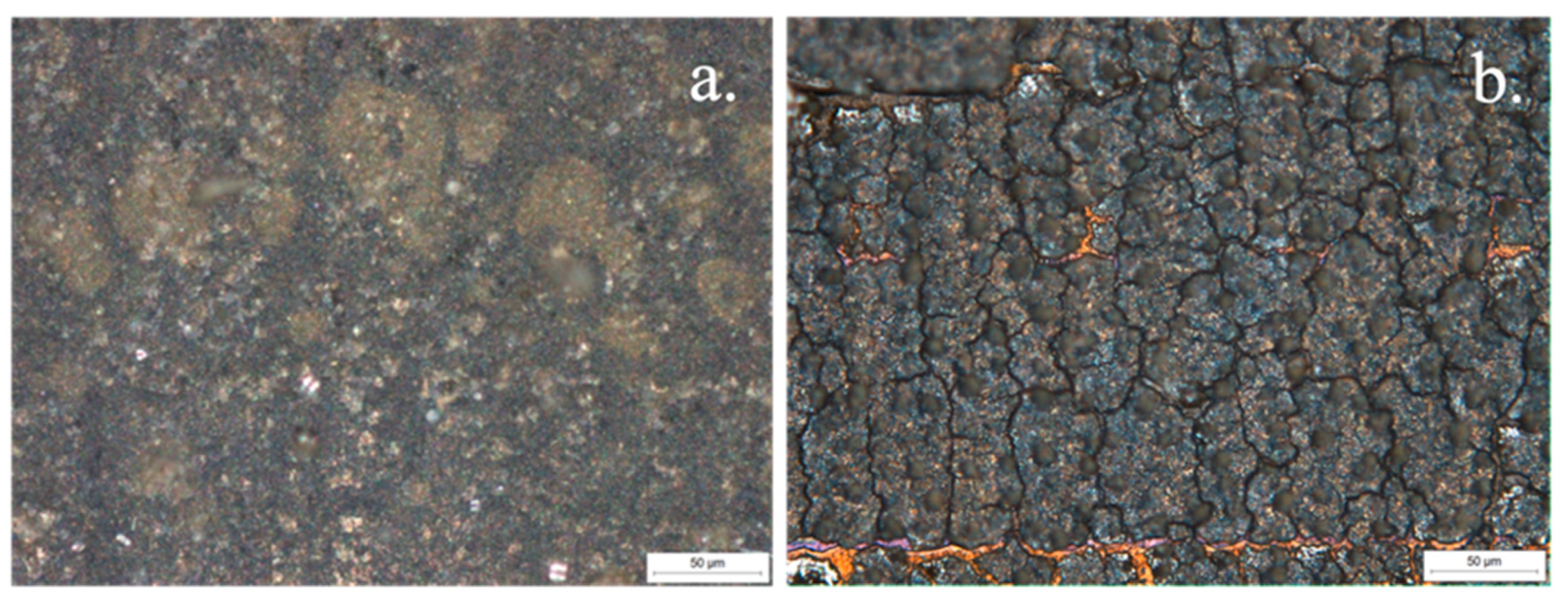
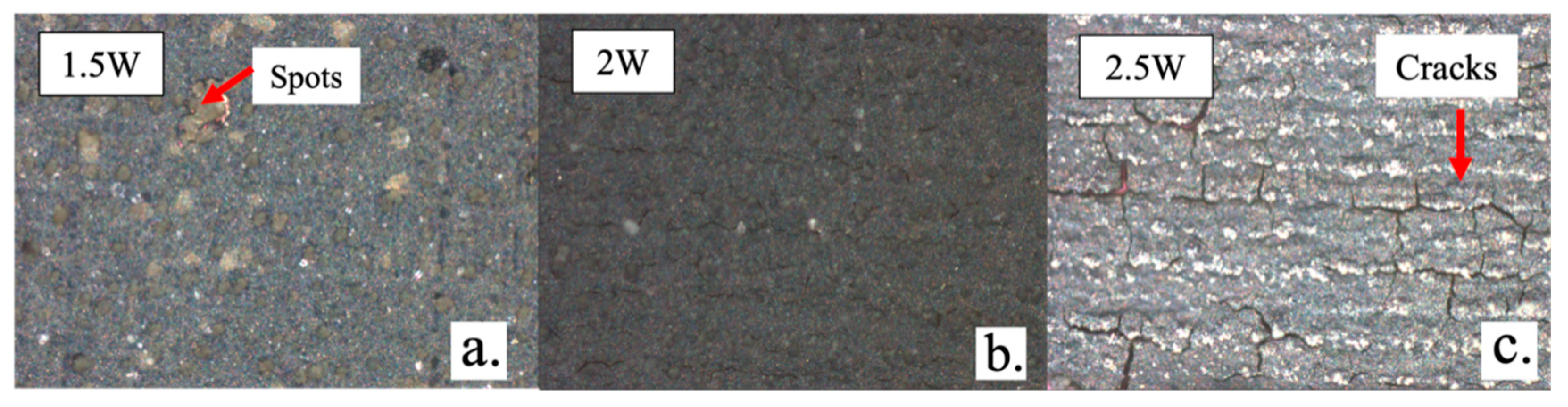
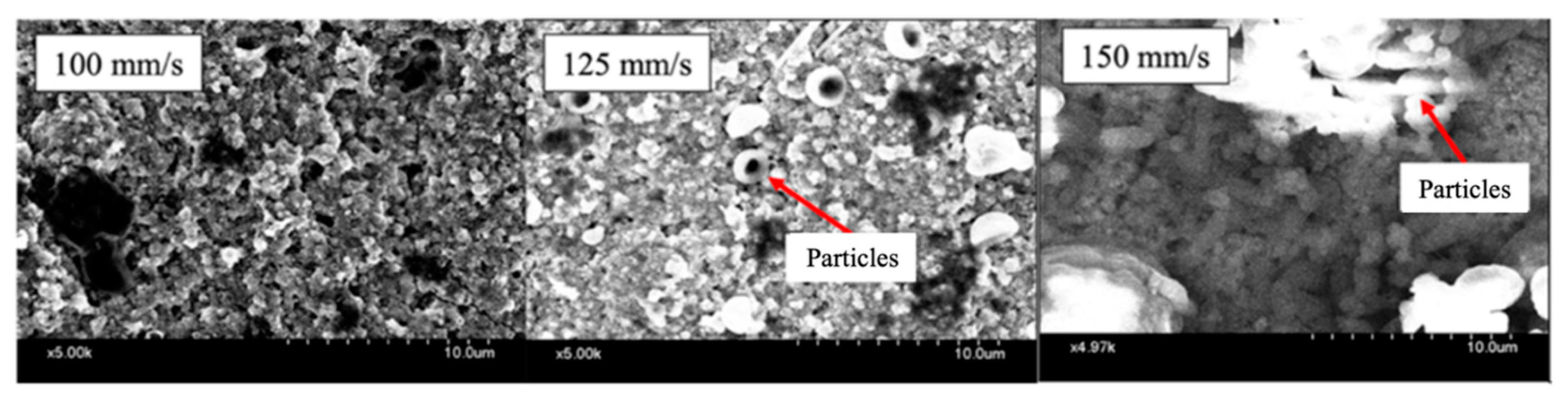
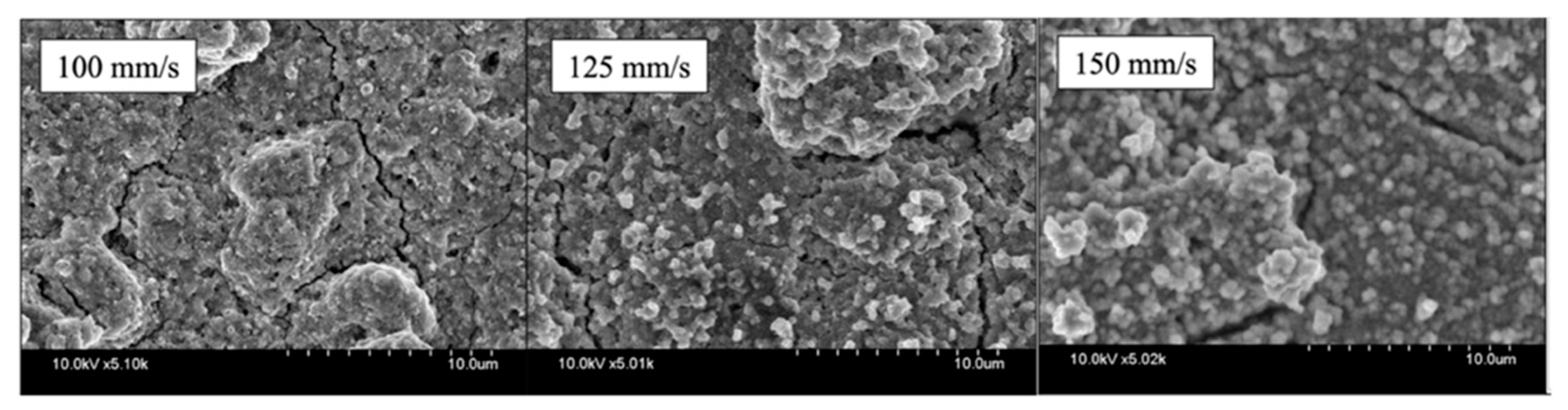
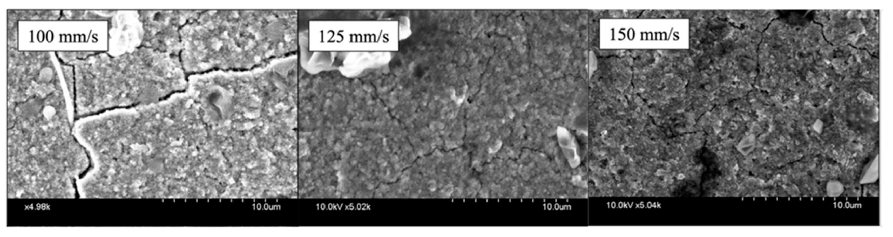
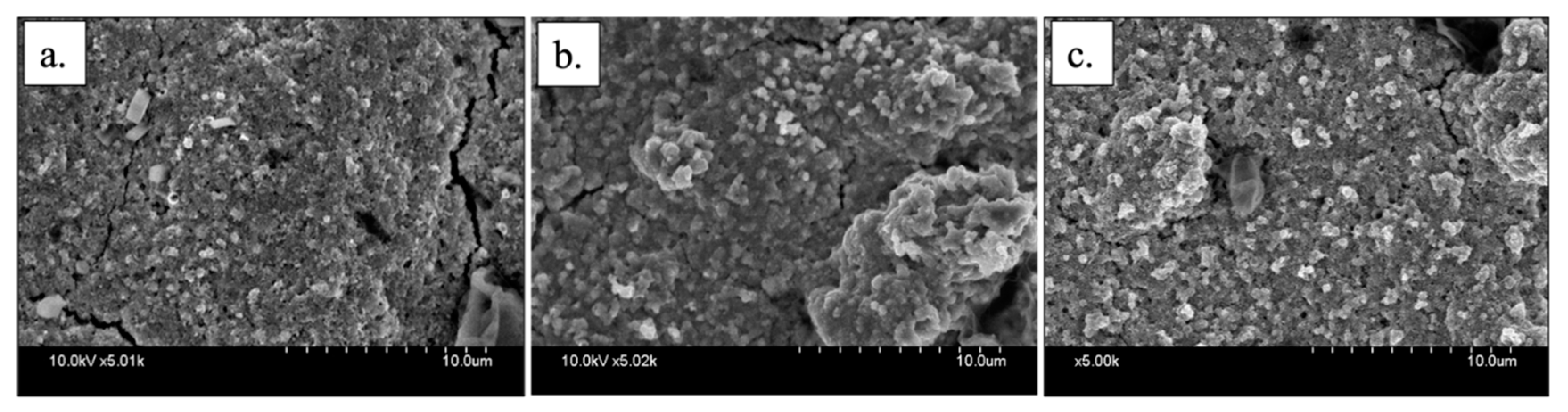
3.2. Morphology of the Printed NiO Thin Films
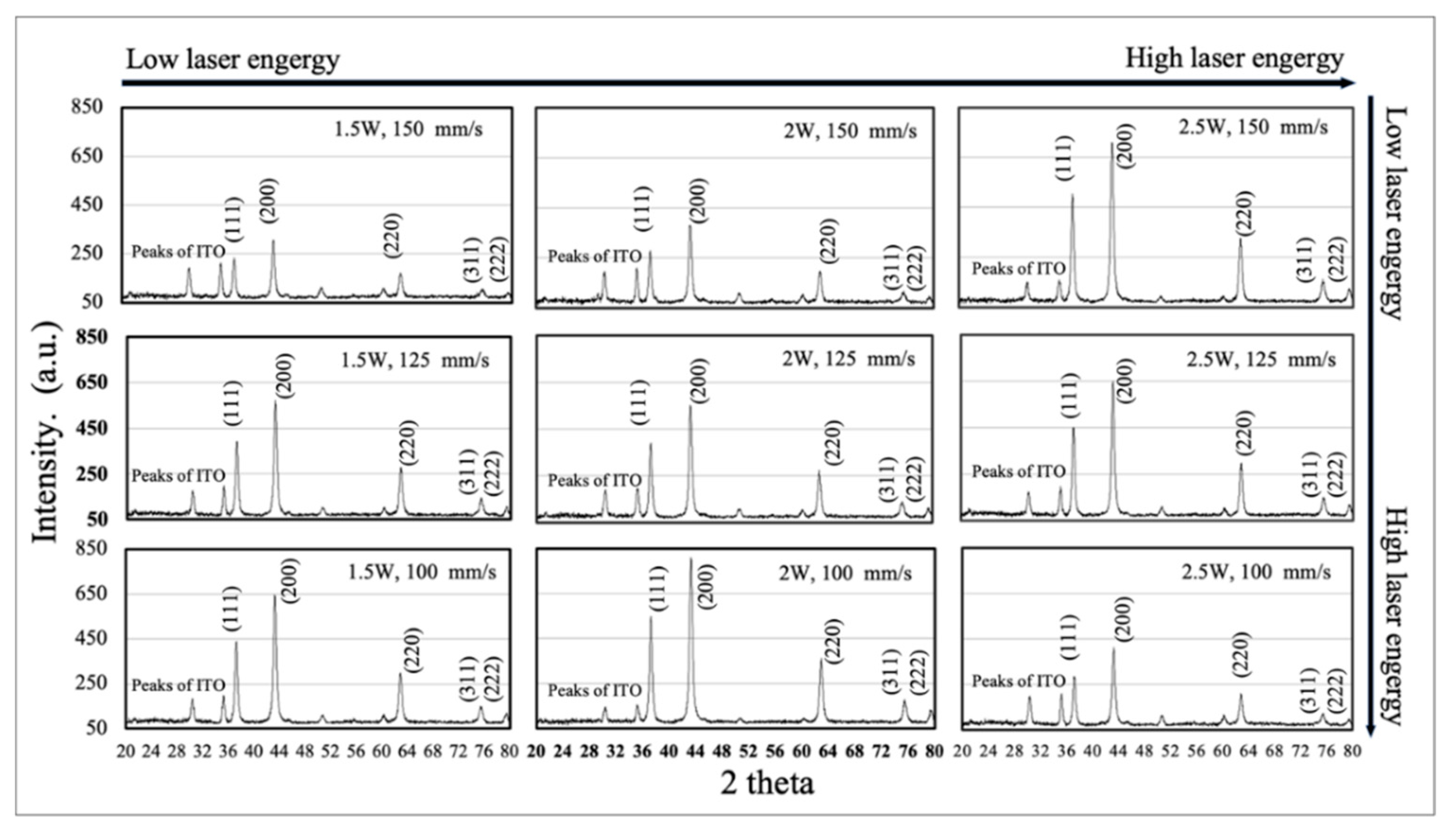
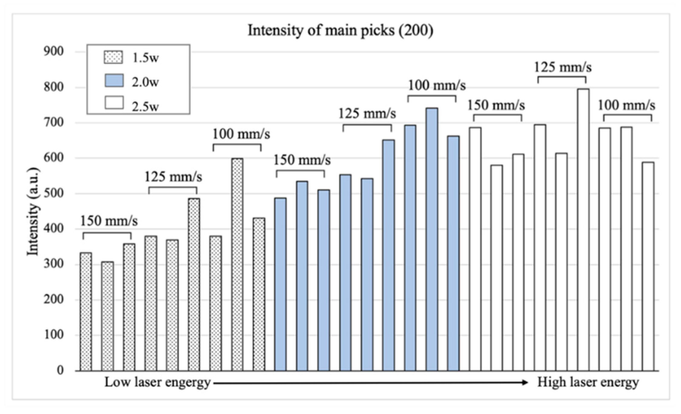
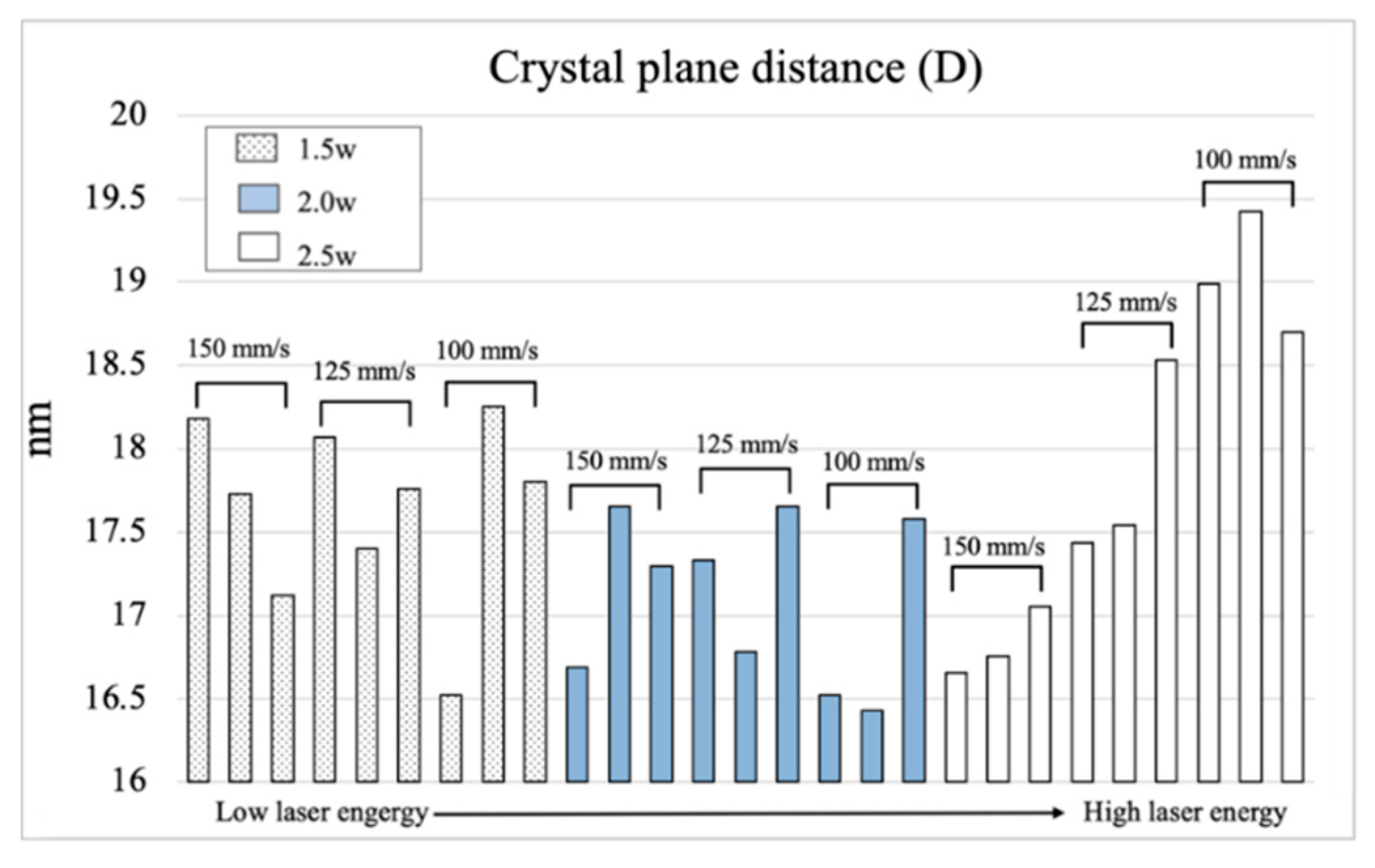
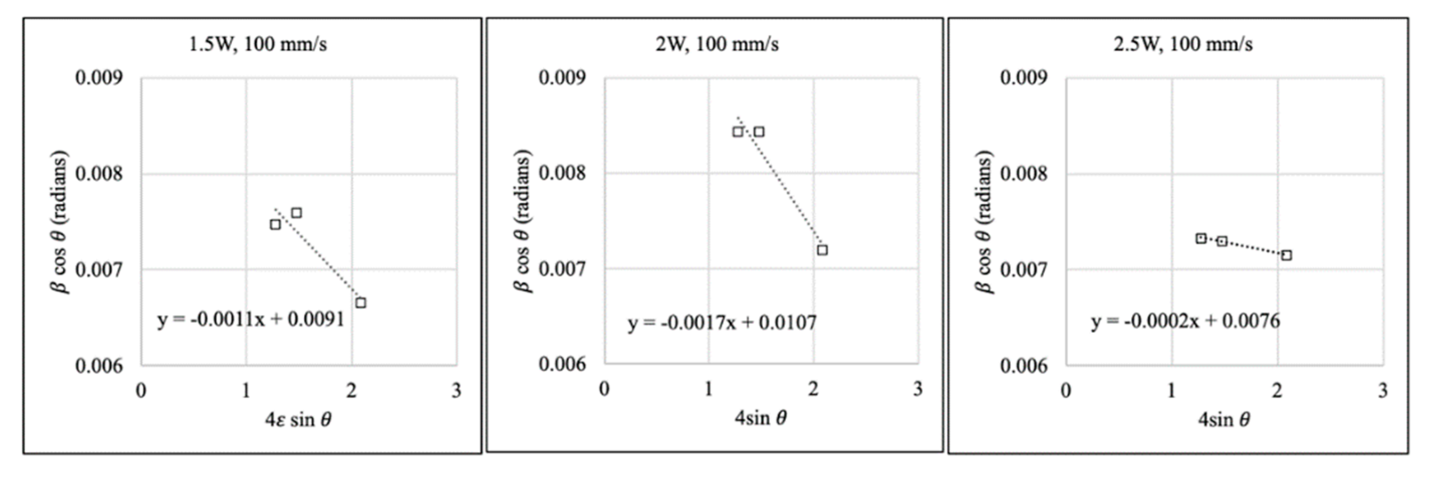
On the basis of the results of electrical properties analysis, laser output was the most influential factor. Therefore, Figure 9 and Figure 10 shows the morphologies of sintered NiO thin films, which were classified by laser output with identical scanning speed (100 mm/s) and frequency (105 k Hz). The confocal microscopy images of the thin films subjected to the 1.5 W output is shown in Figure 9a. The surface exhibited several light color spots, which were residual solution and nonuniform particle accumulation. According to the resistance values with 1.5 W laser output, the laser energy settings were too low to completely sinter the NiO thin films, which caused defects to remain on the surface and high resistance performance. On the other hand, the surface, the 2 W sintered thin film, was even and without visible defects in Figure 9b. According to the aforementioned resistance results, this smooth surface responded to high electrical properties. On the contrary, the significant cracks observed in the NiO thin films subjected to the 2.5 W output (Figure 9c) led to the increase of resistance. In Figure 10, the SEM images with higher resolution provided us with more comprehensive analyses of microscopic morphologies. The SEM morphology of NiO thin film with the 1.5 W output shown in Figure 10 had a porous and uneven surface. Since inadequate sintering energy irradiated on the NiO thin films, the incomplete sintering of original NiO nanoparticles kept the surface rough, causing high resistance. The morphologies were clearly superior in the cases of the 2 W and 2.5 W laser outputs. The surface of the thin film to which the 2 W laser output was applied showed that the particles were joined and merged, while some negligible cracks were observed. Compared with the electrical performance of 1 W and 2.5 W, the electrical properties of 2 W sintered NiO thin films were the greatest. Although the surface of the thin film, to which the 2.5 W laser output was applied, displayed a more even surface, the cracks were obvious, which were sufficiently large to reduce the electrical conduction [30]. Since the adjacent particles were joining together and holes and defects were left at the original positions of the merged particles, the cracks were formed by uneven stress and thus caused the resistance to increase.
To observe the effect of scanning speed variation from each laser output, Figure 11, Figure 12 and Figure 13 show the morphologies that were sintered by 1.5 W, 2 W, and 2.5 W with different scanning speeds, respectively. The SEM photographs of NiO thin films with 1.5 W output are shown in Figure 11. Since the particles were barely sintered, the surfaces of the thin films retained the shape of nanoparticle agglomerations. Moreover, according to the resistance experimental results, the resistances decreased drastically as the speed increased. The significant morphological change illustrated that the sintering process was in an initial stage, where the particles rapidly joined together [31]. Figure 12 shows the micro-surface of the NiO thin films sintered by varied scanning speeds with 2 W. The change of morphologies was not obvious under different scanning speeds. The minor cracks observed on the surface did not extend when the scanning speeds were reduced. According to the resistance experimental results, the effect of tiny cracks on electrical property was negligible. For the 2.5 W laser output, the surfaces were fairly even, and the particles were closely joined together. The level of flatness was even higher than that of the 2 W sintered surface (Figure 13, SEM images). However, the resistances’ performance subject to the 2.5 W output increased, while the scanning speed slowed down. Cracks extended due to excessively high-intensity energy, which eventually affected the electrical conductivity.
As mentioned earlier, the effect of laser frequency variation on the electrical properties in the experiments was not significant. The SEM photographs showed the similar results of frequency’s effect. In Figure 14, NiO thin films were sintered by varied frequencies with 2 W laser output and 150 mm/s scanning speed. The morphologies show that the influence of frequency variation was insignificant not only on resistance and sensitivity but the morphologies. According to Equation (5), the variation of laser frequency should be amplified to efficiently affect the laser sintering performance.

3.3. XRD Analysis

Besides morphology, XRD analyses assisted us to obtain a better understanding of the reaction of UV laser to the NiO particles and the mechanism of cracks. The XRD patterns of NiO thin films are shown in Figure 15. These detected 2θ at 37.2°, 43.3°, 62.9°, 75.5°, and 79.5° respond to the diffraction signals of crystal planes (111), (200), (220), (311), and (222), respectively. Since XRD penetrated the thin films and reflected the signal of ITO electrodes, there were redundant peaks that represented the diffraction of the ITO electrodes and glass substrate at 2θ at 30.32 and 35.22, although the XRD operation was a grazing incidence small angle. Yet, these unwanted signals did not take effect on the NiO peaks and could be ignored. The 2θ results illustrated that there were no redox reactions in NiO, and unpredictable peaks did not appear. Moreover, the diffraction intensities enhanced as the UV laser energy absorption increased. This phenomenon indicated the signals of crystal planes were enhanced because of the increasing combination of particles; however, Figure 15 shows the intensity slightly declined in the experimental group of 2.5 W laser output since the uneven thickness, defects, and strains affected the diffraction intensity [32], causing peak shifting and broadening [33]. Therefore, according to SEM photographs, the micro-strains of 2.5 W sintered thin films were more likely to reduce the diffraction intensity (Figure 16).
In Figure 17, the crystal plane distances exhibited that there was no significant increase while laser energy increased. The maximum difference of crystal plane distances was only approximately 3 nm. There was no obvious recrystallization or growth of the grain in the films since the excessive laser energy damaged the fragile printed thin films easily. However, there was a trend that crystal plane distances slightly declined at laser power 2.5 W while scanning speed accelerated. According to Scherrer’s equation (Equation (2)), the longer crystal plane distances can be stretched; thus, the larger β (FWHM) of peaks are broadened [33]. In the status of no recrystallization occurrence, the strain was the reason that broadens the β (FWHM). Therefore, the strains were built in the NiO thin films during the sintering process in the range of laser energy from 1.5 W to 2 W, causing the crystal plane distances to raise slightly. However, as significant cracks appeared, the stress between boundaries was released. In conclusion, the cause of the varied crystal plane distance was not recrystallization but strains. It eventually formed the cracks, which decreased the electrical conduction of the thin films.
For the mechanism of the strain analyses, the Williamson–Hall plots were drawn to analyze the strain in the thin films. By applying this method, the strain can be acquired from the slope of the linear regression in the plots. Figure 18 shows the examples of the Williamson–Hall plot from results of varied laser output with 100 mm/s scanning speed. The positive slope of linear regression indicated tensile stress in the Williamson–Hall plot. In previous NiO thin film studies, tensile strain frequently occurred while the furnace sintering processes were applied [34,35,36] because of the long calcination time and high furnace temperature, which provided adequate conditions for grain growth. However, the slopes of linear regression were negative in this study, which means the strain of the NiO thin films was compressive strain. In Figure 19, there was a turning point at 2 W, 100 mm/s; the tendency of strain increased with the raising of laser energy and declined after 2.5 W, 150 mm/s. Since the energy merged the nanoparticles together, eliminating the pores among them, a bulk NiO thin film was formed. However, residual strain caused severe nonuniform shrinkage that produced cracks on the NiO nanoparticle thin films because there was no occurrence of recrystallization. From the perspective of SEM images, Figure 20 illustrates the nonuniform shrinkage of compression strain from 2 W and 2.5 W sintered NiO thin films; laser spots induced the volume change of the thin film, resulting in the regional compression strains, which caused tension force among themselves. In Figure 20a, the protruding reginal compression strains were obvious since the NiO thin films were composed by nanoparticles. The thin films had pores and vacancy, which were partially removed by laser spots. The effect of the elimination of defects causes nonuniform compression strain in the films. To improve the electrical properties, the issue of the shrinkage should be solved. Accelerating scanning speed and significantly increasing the frequency of laser pulses might achieve a better sintering state and morphology. Regarding printing technology, if it was not for aerosol jet, which created low roughness of the thin films (approximately 1.6 μm), the uneven compress strain might have been even more severe. Take inkjet, for example, the print nozzle of piezoelectric inkjet intermittently presses the droplets on the substrates, which causes the rough surface [19].

4. Conclusions

The study applied the UV laser to sintering NiO thin film sensors to achieve efficient a manufacturing process involving small batch sizes. Compared to the furnace curing process, laser sintering reduces hours of furnace treatment time to a few seconds. The 355 nm wavelength UV laser was applied in this study. In this study, the 2-W laser output could provide the lowest average of resistance results compared to the other laser energy output settings. The small variations of resistance for 2-W laser output indicated the sintering process was stable. In addition to the resistance results, the optimal laser parameters setting was also determined by the highest sensitivity. The corresponding process parameters were 2-W laser output, 150 mm/s, and 90Hz. Compared to the previous studies involving the furnace curing process in the literature, the resistance of laser-sintered sensors decreased up to 96%, which allowed the NiO thin films thermistor to be easily operated.
SEM and confocal microscopy were used to investigate the relationship between the surface morphology and electrical properties of NiO thin films under different laser outputs. For the 1.5-W laser output, the surface of the thin films retained the shape of the nanoparticle agglomeration. It was indicated that the energy absorption was insufficient. As to 2.5-W, cracks were observed on the surface. Although the thin-film surfaces were even, the resistances were high due to the cracks. To figure out the effect of cracks on resistance, XRD analysis was performed. It was found that the crystal plane distances were not affected by recrystallization but the cracks. Based on the analysis, there were obvious regional compressive stains before the appearance of cracks, and the uneven shrinking strains caused the cracks on the surface as energy irradiation increased.

Author Contributions

Formal analysis, Y.-T.C., K.-Y.H. and C.-H.C.; resources, W.-T.H.; writing—original draft preparation, Y.-T.C.; writing—review and editing, Y.-T.C., H.-T.Y., W.-T.H. and K.-M.L.; supervision, H.-T.Y., W.-T.H. and K.-M.L.; funding acquisition, W.-T.H. All authors have read and agreed to the published version of the manuscript.

Funding

This research was funded by [Ministry of Science and Technology] grant number [MOST 110-2622-E-492-016].

Institutional Review Board Statement

Ethical review and approval were waived for this study due to REASON (please provide a detailed justification).

Informed Consent Statement

Not applicable.

Data Availability Statement

Not applicable.

Conflicts of Interest

The authors declare no conflict of interest.

References

  1. Han, I.Y.; Kim, S.J. Diode temperature sensor array for measuring micro-scale surface temperatures with high resolution. Sens. Actuators A Phys. 2008, 141, 52–58. [Google Scholar] [CrossRef]
  2. Li, K.-M.; Liang, S.Y. Modeling of Cutting Temperature in Near Dry Machining. J. Manuf. Sci. Eng. 2006, 128, 416–424. [Google Scholar] [CrossRef]
  3. Feteira, A. Negative Temperature Coefficient Resistance (NTCR) Ceramic Thermistors: An Industrial Perspective. J. Am. Ceram. Soc. 2009, 92, 967–983. [Google Scholar] [CrossRef]
  4. Mateos, D.; Valdez, B.; Castillo, J.R.; Nedev, N.; Curiel, M.; Perez, O.; Arias, A.; Tiznado, H. Synthesis of high purity nickel oxide by a modified sol-gel method. Ceram. Int. 2019, 45, 11403–11407. [Google Scholar] [CrossRef]
  5. Farbod, M.; Dehbidi, V.K.; Shoushtari, M.Z. Size dependence of optical and magnetic properties of nickel oxide nanoparticles fabricated by electric arc discharge method. Ceram. Int. 2017, 43, 13670–13676. [Google Scholar] [CrossRef]
  6. Hotovy, I.; Rehacek, V.; Siciliano, P.; Capone, S.; Spiess, L. Sensing characteristics of NiO thin films as NO2 gas sensor. Thin Solid Film. 2002, 418, 9–15. [Google Scholar] [CrossRef]
  7. Hotovy, I.; Huran, J.; Spiess, L.; Hascik, S.; Rehacek, V. Preparation of nickel oxide thin films for gas sensors applications. Sens. Actuators B Chem. 1999, 57, 147–152. [Google Scholar] [CrossRef]
  8. John, R.A.B.; Shruthi, J.; Ramana Reddy, M.V.; Ruban Kumar, A. Manganese doped nickel oxide as room temperature gas sensor for formaldehyde detection. Ceram. Int. 2022, 48, 17654–17667. [Google Scholar] [CrossRef]
  9. Kim, S.; Yang, W.S.; Kim, H.-J.; Lee, H.-N.; Park, T.J.; Seo, S.-J.; Park, Y.M. Highly sensitive non-enzymatic lactate biosensor driven by porous nanostructured nickel oxide. Ceram. Int. 2019, 45, 23370–23376. [Google Scholar] [CrossRef]
  10. Ohta, H.; Hirano, M.; Nakahara, K.; Maruta, H.; Tanabe, T.; Kamiya, M.; Kamiya, T.; Hosono, H. Fabrication and photoresponse of a pn-heterojunction diode composed of transparent oxide semiconductors, p-NiO and n-ZnO. Appl. Phys. Lett. 2003, 83, 1029–1031. [Google Scholar] [CrossRef]
  11. Wei, T.-Y.; Chen, C.-H.; Chien, H.-C.; Lu, S.-Y.; Hu, C.-C. A Cost-Effective Supercapacitor Material of Ultrahigh Specific Capacitances: Spinel Nickel Cobaltite Aerogels from an Epoxide-Driven Sol-Gel Process. Adv. Mater. 2010, 22, 347–351. [Google Scholar] [CrossRef] [PubMed]
  12. Wang, D.-W.; Li, F.; Cheng, H.-M. Hierarchical porous nickel oxide and carbon as electrode materials for asymmetric supercapacitor. J. Power Sources 2008, 185, 1563–1568. [Google Scholar] [CrossRef]
  13. Kim, T.W.; Hwang, S.-J.; Jhung, S.H.; Chang, J.-S.; Park, H.; Choi, W.; Choy, J.H. Bifunctional Heterogeneous Catalysts for Selective Epoxidation and Visible Light Driven Photolysis: Nickel Oxide-Containing Porous Nanocomposite. Adv. Mater. 2008, 20, 539–542. [Google Scholar] [CrossRef]
  14. Liu, H.; Wang, G.; Liu, J.; Qiao, S.; Ahn, H. Highly ordered mesoporous NiO anode material for lithium ion batteries with an excellent electrochemical performance. J. Mater. Chem. 2011, 21, 3046. [Google Scholar] [CrossRef]
  15. Seo, S.; Lee, M.J.; Seo, D.H.; Jeoung, E.J.; Suh, D.-S.; Joung, Y.S.; Yoo, I.K.; Hwang, I.R.; Kim, S.H.; Byun, I.S.; et al. Reproducible resistance switching in polycrystalline NiO films. Appl. Phys. Lett. 2004, 85, 5655–5657. [Google Scholar] [CrossRef]
  16. Li, Y.; Zhou, K.; Tan, P.; Tor, S.B.; Chua, C.K.; Leong, K.F. Modeling temperature and residual stress fields in selective laser melting. Int. J. Mech. Sci. 2018, 136, 24–35. [Google Scholar] [CrossRef]
  17. Linares, J.; Chaves-Jacob, J.; Lopez, Q.; Sprauel, J.-M. Fatigue life optimization for 17-4Ph steel produced by selective laser melting. RPJ 2022, 28, 1182–1192. [Google Scholar] [CrossRef]
  18. Khorasani, M.; Ghasemi, A.; Rolfe, B.; Gibson, I. Additive manufacturing a powerful tool for the aerospace industry. RPJ 2022, 28, 87–100. [Google Scholar] [CrossRef]
  19. Huang, C.-C.; Kao, Z.-K.; Liao, Y.-C. Flexible Miniaturized Nickel Oxide Thermistor Arrays via Inkjet Printing Technology. ACS Appl. Mater. Interfaces 2013, 5, 12954–12959. [Google Scholar] [CrossRef]
  20. Chia Wang; Guan-Yi Hong; Kuan-Ming Li; Hong-Tsu Young A Miniaturized Nickel Oxide Thermistor via Aerosol Jet Technology. Sensors 2017, 17, 2602. [CrossRef] [Green Version]
  21. Chang, Y.-T.; Hung, K.-Y.; Young, H.-T.; Li, K.-M.; Chen, R.K. Aerosol jet printing of nickel oxide nanoparticle ink with ultraviolet radiation curing for thin-film temperature sensors. Int. J. Adv. Manuf. Technol. 2021, 118, 1957–1965. [Google Scholar] [CrossRef]
  22. Paeng, D.; Lee, D.; Yeo, J.; Yoo, J.-H.; Allen, F.I.; Kim, E.; So, H.; Park, H.K.; Minor, A.M.; Grigoropoulos, C.P. Laser-Induced Reductive Sintering of Nickel Oxide Nanoparticles under Ambient Conditions. J. Phys. Chem. C 2015, 119, 6363–6372. [Google Scholar] [CrossRef]
  23. Zheng, H.; Li, L.; Yu, S.; Lu, T.; Sun, Z.; Chen, S.; Wu, M. Low voltage driven NiO thin film capacitors for tunable applications. Thin Solid Film. 2019, 669, 151–156. [Google Scholar] [CrossRef]
  24. El-Kemary, M.; Nagy, N.; El-Mehasseb, I. Nickel oxide nanoparticles: Synthesis and spectral studies of interactions with glucose. Mater. Sci. Semicond. Processing 2013, 16, 1747–1752. [Google Scholar] [CrossRef]
  25. Lee, D.; Paeng, D.; Park, H.K.; Grigoropoulos, C.P. Vacuum-Free, Maskless Patterning of Ni Electrodes by Laser Reductive Sintering of NiO Nanoparticle Ink and Its Application to Transparent Conductors. ACS Nano 2014, 8, 9807–9814. [Google Scholar] [CrossRef]
  26. Salary, R.; Lombardi, J.P.; Tootooni, M.S.; Donovan, R.; Rao, P.K.; Poliks, M.D. In Situ Sensor-Based Monitoring and Computational Fluid Dynamics (CFD) Modeling of Aerosol Jet Printing (AJP) Process. In Proceedings of the Volume 2: Materials; Biomanufacturing; Properties, Applications and Systems; Sustainable Manufacturing, Blacksburg, VA, USA, 27 June 2016; American Society of Mechanical Engineers: Blacksburg, VA, USA, 2016; p. V002T04A049. [Google Scholar] [CrossRef]
  27. Kang, J.-E.; Ryu, J.; Han, G.; Choi, J.-J.; Yoon, W.-H.; Hahn, B.-D.; Kim, J.-W.; Ahn, C.-W.; Choi, J.H.; Park, D.-S. LaNiO3 conducting particle dispersed NiMn2O4 nanocomposite NTC thermistor thick films by aerosol deposition. J. Alloy. Compd. 2012, 534, 70–73. [Google Scholar] [CrossRef]
  28. Montgomery, D.C. Design and Analysis of Experiments; John Wiley & Sons: Hoboken, NJ, USA, 2017; ISBN 978-1-119-11347-8. [Google Scholar]
  29. Schnell, G.; Duenow, U.; Seitz, H. Effect of Laser Pulse Overlap and Scanning Line Overlap on Femtosecond Laser-Structured Ti6Al4V Surfaces. Materials 2020, 13, 969. [Google Scholar] [CrossRef] [Green Version]
  30. Ponmudi, T.S.; Lee, C.-W.; Lai, C.-C.; Tsai, C.-H. Comparative study on the effect of annealing temperature on sol–gel-derived nickel oxide thin film as hole transport layers for inverted perovskite solar cells. J. Mater. Sci. Mater. Electron. 2021, 32, 8157–8166. [Google Scholar] [CrossRef]
  31. Coble, R.L. A Model for Boundary Diffusion Controlled Creep in Polycrystalline Materials. J. Appl. Phys. 1963, 34, 1679–1682. [Google Scholar] [CrossRef]
  32. Malliga, P.; Pandiarajan, J.; Prithivikumaran, N.; Neyvasagam, K. Influence of Film Thickness on Structural and Optical Properties of Sol—Gel Spin Coated TiO2 Thin Film. IOSRJAP 2014, 6, 22–28. [Google Scholar] [CrossRef]
  33. Muhammed Shafi, P.; Chandra Bose, A. Impact of crystalline defects and size on X-ray line broadening: A phenomenological approach for tetragonal SnO2 nanocrystals. AIP Adv. 2015, 5, 057137. [Google Scholar] [CrossRef]
  34. Madhu, G.; Bose, V.C.; Maniammal, K.; Aiswarya Raj, A.S.; Biju, V. Microstrain in nanostructured nickel oxide studied using isotropic and anisotropic models. Phys. B Condens. Matter 2013, 421, 87–91. [Google Scholar] [CrossRef]
  35. Biju, V.; Sugathan, N.; Vrinda, V.; Salini, S.L. Estimation of lattice strain in nanocrystalline silver from X-ray diffraction line broadening. J. Mater. Sci. 2008, 43, 1175–1179. [Google Scholar] [CrossRef]
  36. Maniammal, K.; Madhu, G.; Biju, V. X-ray diffraction line profile analysis of nanostructured nickel oxide: Shape factor and convolution of crystallite size and microstrain contributions. Phys. E Low-Dimens. Syst. Nanostruct. 2017, 85, 214–222. [Google Scholar] [CrossRef] [Green Version]
Figure 1. The aerosol jet printer modules. Ultrasonic atomizer (left) and pneumatic atomizer (right).
Applsci 12 07206 g001
Figure 2. (a) ITO interdigital electrodes of partial enlargement with schematic of printing position of NiO thin film. (b) ITO interdigital electrodes on glass substrate.
Applsci 12 07206 g002
Figure 3. The colormaps of confocal microscopy to show the height difference of NiO thin film which were caused by electrodes (a) on ITO electrodes (b) on silver electrodes.
Applsci 12 07206 g003
Figure 4. (a) Microscope photography of 1 W sintered thin film with 100 mm/s laser scanning speed (scale bar 50 μm). (b) microscope photography of 3 W sintered thin film with 100 mm/s laser scanning speed (scale bar 50 μm).
Applsci 12 07206 g004
Figure 5. (a) Experimental setup for NiO resistance measurement. (b) Schematic of measurement setup for NiO thin films characterization.
Applsci 12 07206 g005
Figure 6. Resistance experimental results of all laser parameters that were measured at 35 °C and compared with furnace 260 °C calcination process (far right in each chart).
Applsci 12 07206 g006
Figure 7. Resistance experimental results of all laser parameters that were measured at 100 °C and compared with furnace calcination process (far right in each chart).
Applsci 12 07206 g007
Figure 8. Sensitivity of all laser parameters.
Applsci 12 07206 g008
Figure 9. Confocal microscope photographs (magnification 20× images) of thin films were sintered by same scanning speed and frequency but with different power output. Laser parameters 100 mm/s, 105 k Hz with 1.5W (a), 2W (b) and 2.5W (c).
Applsci 12 07206 g009
Figure 10. The SEM photographs (magnification 5k× images) of thin films were sintered by same scanning speed and frequency but with different power output. Laser parameters 100 mm/s, 105 k Hz with 1.5W (a), 2W (b) and 2.5W (c).
Applsci 12 07206 g010
Figure 11. SEM morphologies of 1.5W sintered thin films with varied scanning speeds.
Applsci 12 07206 g011
Figure 12. SEM morphologies of 2 W sintered thin films with varied scanning speeds.
Applsci 12 07206 g012
Figure 13. SEM morphologies of 2.5 W sintered thin films with varied scanning speeds.
Applsci 12 07206 g013
Figure 14. SEM morphologies (magnification 5k×) of 2W sintered thin films with scanning speed 150mm/s, and frequencies 90 k Hz (a), 105 k Hz (b), and 120k Hz (c).
Applsci 12 07206 g014
Figure 15. XRD patterns of sintered NiO thin films, which were sintered by different laser power outputs and scanning speeds. The results illustrated that there were no redox reactions in NiO, and unpredictable peaks.
Applsci 12 07206 g015
Figure 16. Intensity of main picks of all laser output parameters.
Applsci 12 07206 g016
Figure 17. Crystal plane distance of all laser parameters.
Applsci 12 07206 g017
Figure 18. Williamson−Hall plots of NiO thin films, which were sintered by 1.5 W, 2 W, and 2.5 W, with 100 mm/s laser scanning speed (the squares were from XRD peaks 111, 200 and 220).
Applsci 12 07206 g018
Figure 19. Strain results of all laser output parameters.
Applsci 12 07206 g019
Figure 20. (a) 2-W laser output causes reginal compression strain; (b) excess reginal strains result in significant cracks, which were created by 2.5-W laser output.
Applsci 12 07206 g020
Table 1. Detailed information of non-sintered NiO nanoparticle thin films as fabricated by aerosol jet.
Raw NiO Thin FilmsAverage Thickness of NiO Thin FilmsResistance at 100 °C Height of Satellite Particles Average of Roughness
15 μm106.8 MΩ1~5 μm1.63 μm
Table 2. Laser parameters experiments setting.
Laser ParametersSetting
Distance (lens-thin film) Out of focus (150 mm)
Laser power output1.5 W, 2 W, and 2.5 W
Frequency (kHz)90, 105, and 120
Scanning speed100 mm/s, 125 mm/s, and 150 mm/s
Laser trajectory spacing5 μm
Publisher’s Note: MDPI stays neutral with regard to jurisdictional claims in published maps and institutional affiliations.

