Article

A High-Throughput Vernier Time-to-Digital Converter on FPGAs with Improved Resolution Using a Bi-Time Interpolation Scheme

1
School of Mechanical Engineering, Nanjing University of Science and Technology, Nanjing 210094, China
2
Science and Technology on Electromechanical Dynamic Control Laboratory, Xi’an 710000, China
3
Shanghai Aerospace Control Technology Institute, Shanghai 201109, China
*
Author to whom correspondence should be addressed.
Appl. Sci. 2022, 12(15), 7674; https://doi.org/10.3390/app12157674
Submission received: 3 July 2022 / Revised: 25 July 2022 / Accepted: 27 July 2022 / Published: 29 July 2022

Abstract

:
A novel ring oscillator-based Vernier-type time interpolation method, known as the fine-timestamp maker, is proposed for field programmable gate array (FPGA)-based time-to-digital converters (TDCs). This method determines lower measurement dead time and improves resolution by using a bi-time interpolation scheme, first presented in this paper. Additionally, a group of cascaded delay units are packaged as an intellectual property core (DU-IP) to form a ring delay line and to adjust its length via the engineering change order (ECO) tool, which makes the adjustment of the ring oscillator’s frequency more linear and less position dependent. A prototype TDC was implemented on a Kintex-7 FPGA. The experimental results demonstrate that a single TDC channel only consumes 35 DFFs, 31 LUTs, and 16 CARRY4 logics after specific adjustment. The results, with a time resolution of 20 ps, dead time of 58 ns, and a root-mean-square error of 15–20 ps, show a significant performance improvement compared to traditional Vernier-type TDCs.

1. Introduction

Time-to-digital converters (TDCs) are core components of timing-related systems and are used to convert a time interval into a digital one with sub-nanosecond accuracy. Initially, TDC technology was investigated in high-energy nuclear science experiments to measure charged-particle time-of-flight (ToF) [1]. Then, momentum and trajectory data were obtained to determine the particle type [2,3]. TDC is often used in other fields, such as positron emission tomography (PET) [4], laser radar [5], and all-digital phase-locked loops [6].
Currently, TDCs are primarily implemented on either application-specific integrated circuits (ASICs) or field-programmable gate arrays (FPGAs). Although ASIC-based TDCs can achieve picosecond-level precision [7], the unique reconfigurability of FPGA technology makes its design extraordinarily flexible. Additionally, with the continuous development of FPGA technology, cost performance has been continuously improved so that FPGAs are excellent for low development cost and fast prototyping [8]. Therefore, FPGA-based TDCs have become more and more popular in the past decade [9,10,11,12,13,14,15,16,17,18,19,20,21,22,23].
A typical FPGA-based TDC structure contains a coarse counter and a time interpolation module. The former provides a more extended measurement range, which runs at the system clock rate, and the latter yields a sub-clock period resolution. Then, the coarse timestamp (given by the coarse counter) and the fine timestamp (given by the time interpolation module) are combined to obtain the timestamp representing the moment when a hit signal arrives. The time interpolation method of FPGA-based TDCs is mainly focused on the tapped delay line (TDL) [9,10,11,12,13,14,15,16,17], which exploits the fast carry-chain resources inside the FPGA as a delay unit to form a long delay line, covering one system clock cycle. However, ultra-wide bins, which are natural TDL and TDC bottlenecks, inevitably deteriorate the time resolution, differential nonlinearity (DNL) error, and integral nonlinearity (INL) error. To extend the resolution beyond its intrinsic cell delay, researchers have been investigating WU-A and WU-B methods proposed by Wu in 2008 [10], as the accuracy could be enhanced to less than 10 ps [13,15]. However, its DNL is more than two least significant bits (LSBs). In addition, to achieve a desirable resolution, relatively long delay lines (including more than 100 delay units) must be built, which would consume a lot of the FPGA’s internal resources. Therefore, TDL-based TDCs are not the best choice due to the performance of DNL and resource cost. It is necessary to find a TDC structure that would be well balanced in terms of resolution, dead time, and resource consumption for medium performance requirements.
From a structural point of view, there are mainly two resource-saving time interpolation methods of FPGA-based TDCs. Firstly, the multi-phase clock TDC samples the hit signal simultaneously via a few phase-shifted clocks. The result indicates the fine timestamp of the hit signal. Since multi-phase clocks are easy to implement in FPGA and are almost insensitive to changes in temperature and supply voltage, this method has a short dead time and better DNL performance. However, because the setup time is challenging for high-frequency systems, a relatively poor resolution (between 80–100 ps) is obtained, limiting the range of applications [18,19,20]. Secondly, the ring oscillator (RO) method follows the Vernier principle and saves resources by folding the TDL’s long carry-chains into a looped structure. Its resolution is the period difference between two ROs working in Vernier mode. Smaller DNL and INL (less than one LSB) will be obtained due to the disappearance of the ultra-wide bins. This method could have potentially achieved a resolution of lower than 10 ps. However, since the uncompensated delay jitter accumulates gradually when the oscillation number increases, the root-mean-square error (RMSE) will worsen proportionally and greatly limit the achievable resolution. Thus, measurement results will be meaningless when the RMSE is greater than one LSB. To avoid this effect, the key to improving this TDC structure’s performance is to reduce the required oscillation number without changing the resolution goal.
Cui and Li [23] proposed a method of bidirectional operation on the Vernier delay lines, which could halve the oscillation number, but with double the resources consumed and a long dead time. In summary, the few tentative studies based on Vernier-type TDC did not thoroughly investigate methods to improve resolution, dead time, and resource consumption simultaneously, i.e., when the selected resolution is small, the resource consumption and dead time are large, and vice versa [21,22,23]. These are the cases that significantly limit the practical applications.
This study proposes a fine-timestamp maker that uses a bi-time interpolation scheme (first presented in this paper), to alleviate resolution problems without adding extra resource consumption and dead time. Therefore, a relatively high-precision and high-throughput Vernier-type TDC would be achieved. Typically, the TDC’s resolution is adjusted by the multiplexer or recompilation processes; instead of this approach, we design a linearly adjustable RO structure packaged as an IP core with less position dependence, to ensure the ideal resolution can be selected. Previous publications on FPGA-based Vernier TDC mainly adopt two ring oscillators working in Vernier mode [21,22,23], and its resolution is the period difference between two ring oscillators. Taking the system clock as the reference, this paper only needs one ring oscillator so that some factors incurring metastability risk can be avoided, which will also save the resource consumption of one RO. In conclusion, due to the resource-saving characteristics of the proposed method, the TDC design can attain an excellent multi-channel capability to realize more functions. Additionally, a resource-saving TDC structure with balanced performance can also achieve an ideal power consumption.
The remaining structure of this paper is as follows. Section 2 describes the principle and structure of the fine-timestamp maker, including its composition, circuitry, and performance evaluation. Section 3 presents the design and time-interval experiments of the TDC. Section 4 discusses the experimental results and outlook on future research. Section 5 provides a summary and conclusions.

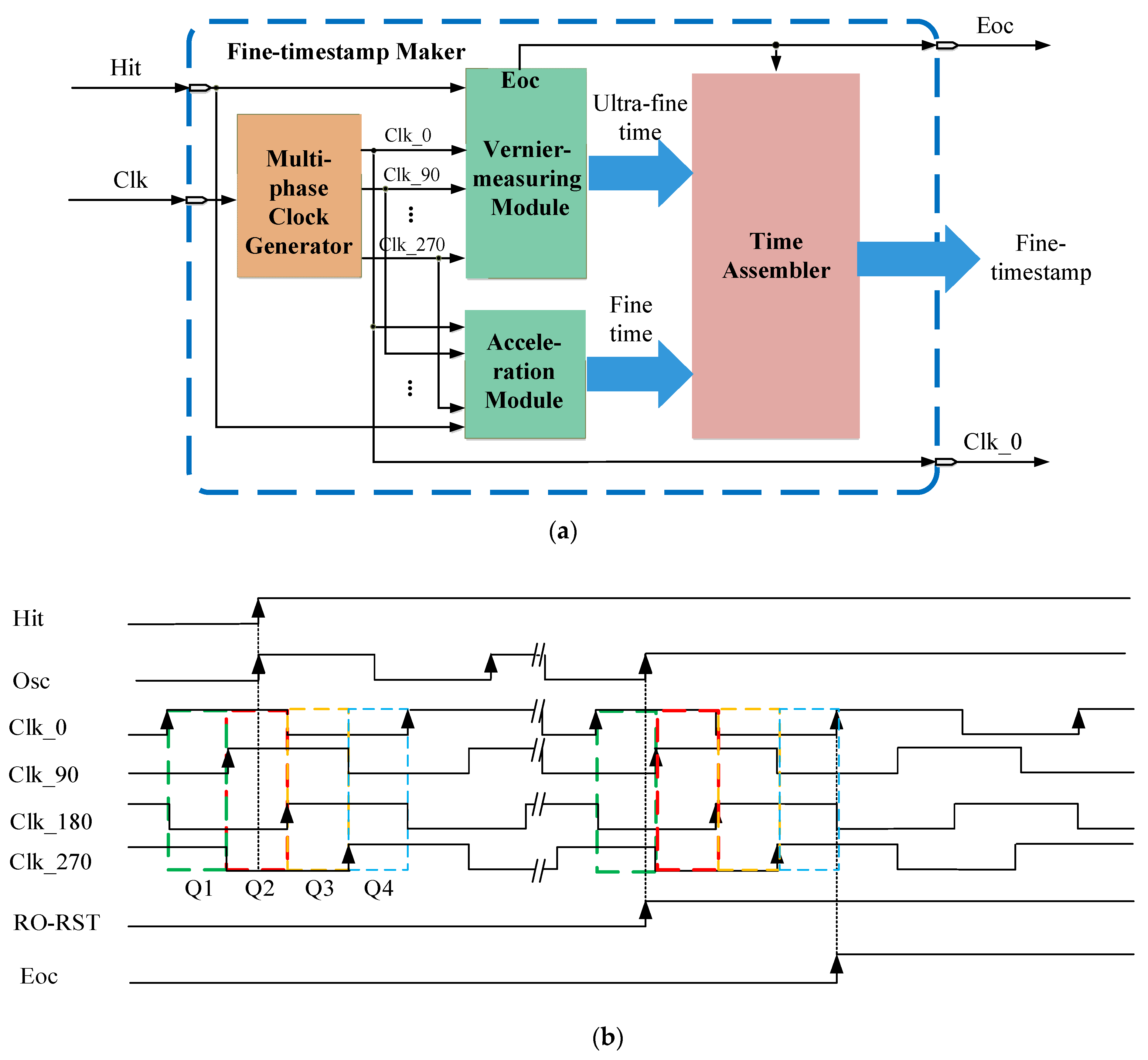
2. Fine-Timestamp Maker Design

2.1. Architecture and Circuit Design

The fine-timestamp maker measures the time interval between the hit signal and the system clock’s preceding rising edge; the complete circuit structure is shown in Figure 1a. It mainly contains two steps of time interpolation. First, one acceleration module primarily aims to reduce the maximal working time of the Vernier-measuring module and preliminarily interpolate the whole period of the system clock via four multi-phase clocks. However, the measurement result, called fine time, has a relatively lower resolution. Second, to achieve higher measurement precision, one Vernier-measuring module is investigated to interpolate fine time again for the ultimate resolution. It determines the highest measurement capabilities of the TDC in this design.
When the Eoc (representing the end of conversion) signal becomes one, the time assembler combines the fine time and the ultra-fine time as the fine timestamp representing the time interpolation results. The entire process flows are shown in Figure 2. Additionally, the multi-phase clock generator (via the phase-locked loops (PLLs) inside the FPGA) synthesizes the input clk signal (provided by a differential active crystal oscillator of 500 MHz) to generate four outputs (clk_0-clk_270) with the same frequency but at 90-degree phase shifts from each other, where clk_0 is the system clock signal of the whole TDC.
The main principle of the acceleration module shown in Figure 3 is that the four phase-shifted clocks directly sample the hit signal simultaneously. When the rising edge of the hit signal arrives, one clock cycle of the system clock clk_0 is divided into four regions according to the results of Q1–Q4, as shown in Figure 1b. Therefore, if using these region boundaries to stop the Vernier-measuring module, its maximal process time could be reduced by a factor of four, thus, the performance of RMSE could be improved significantly for the same resolution goal. Using the method in [20], Q1–Q4 can be synchronized to the system clock clk_0 within three clock cycles, and the four-bit one-hot code can be converted into a two-bit binary code as the fine time, i.e., the first time interpolation is finished. However, its resolution is only in the unit of ¼ of the system clock period.
The composition details of the Vernier-measuring module are shown in Figure 4, which mainly consists of a ring oscillator (RO), an ultra-fine counter, and a coincidence circuit. This module exploits the single ring oscillator working in Vernier mode to generate the ultra-fine time representing the TDC’s highest resolution. The RO is triggered by the hit signal to start oscillation (Osc). Instead of two ROs as used in [21,22,23], the system clock signal clk_0 is directly used as the reference clock signal, so that some factors incurring metastability risk can be avoided. In addition, as the structure of the Vernier-measuring module becomes simpler, it can save the resource consumption of one RO and the position dependence would also be reduced.
The principle of the Vernier-measuring module requires the oscillation period to be different from the reference clock signal (clk_0), then the rising edge of the oscillation signal will gradually move from one region of clk_0 to an adjacent region. The coincidence circuit is designed to determine whether the rising edge of the oscillation signal crosses over any region boundaries of the clk_0 signal as shown in Figure 1b. After they become aligned, the coincidence circuit immediately issues the RO-RST signal to reset the RO and avoid the accumulations of the jitter. After clk_0 synchronizes the RO-RST signal, the end of the current conversion (Eoc) signal is also sent out. In this process, the eight-bit ultra-fine counter records the number of oscillation cycles continuously, and its result also indicates the ultra-fine time in units of the period difference between the oscillation signal and clk_0. Taking the case shown in Figure 1b as an example, the acceleration module indicates that the rising edge of the oscillation signal is in the second of the four regions of clk_0. The oscillation frequency is slightly faster than that of clk_0. Therefore, when the rising edge of the oscillation signal becomes aligned with the first region of clk_0 after a few clock periods, the coincidence circuit immediately sends out the RO-RST signal to stop the RO from initiating oscillation and stop the ultra-fine counter from counting. Therefore, the delay jitter accumulations could be controlled as early as possible. The coincidence circuit then sends an Eoc signal to the time assembler, which means the fine timestamp is ready for output, i.e., the second time interpolation is finished.
The specific implementation of the coincidence circuit is shown in Figure 5. Where the rising edge of the oscillation signal samples each phase-shifted clock, the successive sampling results of the two cascaded flip-flops are output through an XOR gate (S1–S4). When the rising edge of the oscillation signal moves from one region of clk_0 to another, as shown in Figure 1b, we can detect the alignment between the oscillation rising edge and the region boundary by connecting S1–S4 with a four-input OR gate. Two flip-flops, FF0 and FF1, and one AND gate prevents the error that occurs when the RO-RST directly becomes one for the first sampling. The RO-RST signal is output as the Eoc signal after being synchronized by the system clock clk_0.

2.2. Ring Oscillator Design

The TDC’s ultimate resolution is determined by the frequency difference between the ring oscillator and the system clock, clk_0. Since the frequency of clk_0 is constant, the oscillation frequency must be controlled accurately to achieve an ideal resolution of TDC. Therefore, the RO plays an essential role in the Vernier-measuring module.
The traditional structure of an RO is shown in Figure 6 [21,22,23]. Its elemental compositions are the cascaded delay units connected in a looped structure through a NAND gate, where the delay units are the dedicated fast carry-chains in the FPGA. Each delay unit is connected to the n-input multiplexer so that the ring delay line’s actual length could be selected conveniently by changing the four-bit control word (Sel in Figure 6) via the PC. Due to the fast propagation attribute of the delay unit, the frequency of the ROs can be controlled finely. However, the addition of multiplexers incurs a more complex layout and routing of the RO, introducing variable delay fluctuations when they are implemented in different locations on the FPGA.
The most commonly used oscillation frequency adjustment method is via a multiplexer; in this paper, we conduct the comparison test using both this method and RO-IP. As shown in Figure 7, the PC is used to adjust the parameters of both ring oscillators to be tested via USB. The frequency of oscillation output by RO-IP and the traditional method can be observed using a high-bandwidth (1.5 GHz) oscilloscope (Tektronix MSO46 made in U.S.A.).
The oscillation period statistics of the conventional method are depicted in the red curve in Figure 8. The Figure 8 indicates many unreasonable situations have occurred, such as the oscillation period generated by the RO with more delay units is smaller than those with fewer delay units. It means that there is a non-negligible difference in the delay between the delay units and the multiplexer when different Sel values are selected. Although the period of oscillation is mainly trending upward as the Sel value increases, its actual delay value fluctuates wildly when adjusting it.
To make the oscillation period more insensitive to the different implementation locations in FPGA, we should use simpler peripheral circuits as much as possible. Based on this principle, we propose a new delay unit cascading structure called “DU-IP”, consisting of only 16 cascaded delay units as shown in Figure 9. Instead of using the multiplexer, we adjust the length of the ring delay line through the engineering change order (ECO) tool in the Xilinx Vivado design suite without the process of re-layout.
In addition, to ensure that the delay units cascaded inside the DU-IP remain in the same relative position with a different layout, we use a relatively paced macro (RPM) tool in Vivado. In this work, we position each delay unit in the DU-IP next to each other (as shown in Figure 10) so that the delay between them is almost consistent, allowing the oscillation period to be adjusted more linearly. Then, we package these relative position constraints of the delay units to form an IP core (intellectual property core). The end users only need to instantiate this IP core when they use it. The absolute position of the DU-IP in the FPGA must then be determined.
The delay units can only be cascaded upwards, but there is a larger gap for every 25 configurable logic blocks (CLBs) in each clock region’s CLB columns. We adopt the manual routing method (setting the P block constraint) during the instantiation process of the DU-IP to ensure that the starting position of the cascaded delay units is implemented as far from the bottom of the clock region as possible. Therefore, those cases where the cascaded delay units in DU-IP generate ultra-wide bins due to spanning across these gaps or even two clock regions can be avoided. As shown in the blue curve in Figure 8, the adjustment of the oscillation period is improved when using the DU-IP in this paper.

2.3. Performance Evaluation

One fine-timestamp maker was implemented on a homemade development board with a Xilinx Kintex-7 FPGA (xc7k325tfgg900 made in U.S.A.). We conducted a code density test via an arbitrary waveform generator to evaluate its various performances. Following this, the hit signals were generated with a frequency of 100.11 KHz to ensure there was no relation to the system clock and fed into the FPGA through the SMA connector. Hence, the time distance to be measured by the fine-timestamp maker is evenly distributed across one clock cycle. Accordingly, the bin widths in the fine-timestamp maker are proportional to the number of hit signals that fell into these bins. Let the actual bin width be W, the total number of samples input in the code density test be N, and n is the number of hit signals falling into these bins. Then,
W = n Δ T max N
where Δ T max represents the maximum working time of a certain module. This code density test was conducted at an ambient temperature of 20 °C with a sample size of one million. Theoretically, the width of each bin should be the resolution of the TDC, but not all bin widths are equal due to some noise and jitter. Therefore, differential nonlinearity (DNL) error and integral nonlinearity (INL) is introduced to quantify these differences. The DNL is defined as the difference between actual bin width and standard bin width, and the INL is defined as the summation of the DNL from the first bin to the current bin. The performance evaluation of the fine-timestamp maker includes two parts: the acceleration module and the Vernier-measuring module. The DNL and INL of the acceleration module are shown in Figure 11, where the DNL ranges from −0.15 LSB to 0.14 LSB, and INL ranges from −012 LSB to 0.15 LSB.
It seems that the measurement accuracy of the Vernier-measuring module could become better when a higher resolution is selected. However, since it will incur a larger oscillation number and jitter accumulations for the same working time, the worsening RMSE could not be ignored. The RMSE value of the Vernier-measuring module is shown in equation [21]:
σ = k Δ T max r e s T c y c = k σ 0
where k is a circuit-dependent constant factor only affected by the whole circuit noise. The res represents the resolution of ultra-fine time and Tcyc is the oscillation period of ROs. σ 0 is the measurement error factor (the larger the value means the larger the measurement error under the same circuit).
In this design, since the reference clock signal for the ring delay line is the system clock signal with a constant period of 2000 ps, then Tcyc = 2000 − res. Accordingly, reducing the Δ T max for the same resolution goal plays a crucial role in the improvement of the measurement error factor σ 0 . For the conventional RO-based TDCs [21,22,23], the maximum working time for Δ T max to be measured by the Vernier-measuring module is the entire clock period of the system clock. In this study, with the help of the acceleration module, the clock period of the system clock could be divided into four parts (as shown in Figure 1b). The value of Δ T max is only T clk /4, and the σ 0 of the Vernier-measuring module could also be reduced by half for the same res target. We could potentially select the double higher resolution without worrying about its RMSE exceeding 1 LSB. Previously, a more appropriate resolution was between 30 ps and 40 ps to ensure a reasonable RMSE [21]. Note that this resolution range will be reduced to 15–20 ps now. When the number of delay units in DU-IP is six, the period of oscillation is approximately 1979 ps, the closest to the optimal resolution range.
According to the code density test, the result statistics from the ultra-fine counter are shown in Figure 12. Its count range is between three and 27. There are 25 bins in ultra-fine time and its standard bin width (i.e., the TDC’s ultimate resolution) is 500 ps/25 = 20 ps.
The DNL and INL results of the Vernier-measuring module are shown in Figure 13, where DNL ranges from −0.51 LSB to 0.06 LSB, and INL ranges from 0 LSB to 0.94 LSB.
The dead time of the acceleration module is three system clock cycles. The maximum oscillation number in the Vernier-measuring module is 27 and the minimum number is three. Additionally, the coincidence circuit needs two additional clock cycles to complete its work. So, the dead time of the Vernier-measuring module is 29 clock cycles. Then the maximum dead time of the fine-timestamp maker is 58 ns.

3. Results

3.1. TDC Design

The fine-timestamp maker is only used to achieve the time interpolation covering the whole period of the system clock. A coarse counter is needed to ensure the TDC obtains a more extensive dynamic measurement range. The coarse-timestamp with a resolution of the system clock period generated by the coarse counter is combined with the fine timestamp in Section 2 to form the ultimate measurement of the moment when a hit signal arrives (i.e., the timestamp of the hit signal), the complete flow of which is shown in Figure 14.
Using the ring counter run at the system clock signal, which is automatically cleared to zero and starts counting again, the start and stop signals are synchronized with the system clock for each latch of a coarse timestamp. The difference between these coarse timestamps is the coarse time. This work uses the Eco signal to retrieve the coarse timestamp.
Since the bin widths of both the fine time and ultra-fine time are not equal everywhere, an offline bin-by-bin calibration is required to improve the measurement accuracy of the TDC. The timestamp (t) is calculated as shown in Equation (3):
t = { ( c u ) T clk + j = 1 m 1 W j + ( i = 1 u 1 W i + W u 2 ) ,   T osc < T clk ( c u ) T clk + j = 1 m W j ( i = 1 u 1 W i + W u 2 ) ,   T osc > T clk
where c is the coarse counter count result, u is the ultra-fine counter count result, m is the fine time result, and Tosc is the period of oscillation.
Two identical TDC channels are necessary to measure a time interval, one measuring the timestamp of the start signal and the other measuring the stop signal. The difference between the two timestamps is the measured time interval.

3.2. Time Interval Test Results

The compilation results show that one TDC channel consumes 35 DFFs, 31 LUTs, and 16 CARRY4 logics, with a less than 0.02% resource occupation rate. We conducted a time interval test to evaluate the RMSE performance of one TDC channel. In the time interval test, we used two channels of the arbitrary waveform generator to provide the start and stop signals. Their time interval was selected by adjusting the start and stop signal phases. To reduce the effect of statistical errors, the sample number for each experiment was 500,000. First, we tested a moderately long time interval; its distribution histogram of measurement results is shown in Figure 15, with a mean value of 15,521 ps and an RMSE of 18.9 ps.
In addition, a time interval test every 1.375 ns in the range of 0 to 30 ns was conducted to observe the performance of the TDC when measuring time intervals of different lengths. The test results are shown in Figure 16, and both the resolution and RMSE could reach the level of 15–20 ps when using the new methods presented in this paper.
The effect of temperature is almost negligible for the acceleration module [20]. Additionally, for the Vernier-measuring module, its Vernier-type delay line is affected by the temperature to a very small extent, approximately 0.1 ps/°C [21]. Therefore, it is unnecessary for this design to adopt any corrections that balance the measurement errors caused by different operating temperatures. To verify the reliability of the experimental results, we add the performance analysis of the proposed method when mounted on different FPGA models (Artix-7). Additionally, we also provide the performance comparison to similar works as shown in Table 1.

4. Discussion and Future Work

Theoretically, the bin widths of the Vernier-type TDC could have been significantly uniform due to the absence of ultra-wide bins. However, according to the performance evaluation results of the fine-timestamp maker, the bin widths at the back part of the ultra-fine counter (25~27) show a remarkable decrease compared with those of other counting ranges (as shown in Figure 11 and Figure 12). This could incur poor DNL performance. As the delay of RO in this design is not compensated, its jitters will gradually accumulate with the increases of the oscillation number. Accordingly, for the hit signals falling into different bins, their position determinations also have different uncertainties. This phenomenon causes some hit signals to be captured by other adjacent bins instead of their target bins. Although the bins located in front will lose some hit signals due to these uncertainties, they will also receive hit signals from neighboring bins as compensation, so it seems that the bin widths in front are generally uniform. Thus, the compensation from adjacent bins will be less than others, and there is a large jitter due to the previous accumulation; the last three TDC bins are therefore more likely to miss their hit signals. For these uneven widths of bins, this study adopts the bin-by-bin calibration method, but both the online and offline calibrations will consume a lot of block RAM resources inside the FPGA. In addition, improving the linearity of the ring oscillator by using the Xilinx Engineering Change Order (ECO) tool in this paper offers significant benefits, but also introduces the drawback of manual tuning of the FPGA bitstream, limiting its potential for large-scale use. Therefore, to further improve the performance of the TDC, we can investigate a jitter compensation method of the ring oscillator and a method that does not require manual adjustment when configuring the ring oscillator length accurately in the subsequent work.
In conclusion, due to low resource consumptions, we could achieve multi-channel designs of TDC to perform more functions. For example, multiple channels measuring the same hit signal simultaneously could improve measurement accuracy, and the multiple channels taking turns to measure different hit signals could reduce the dead time. Note that the existing design in this work is the result of a trade-off between the performance of resolution, resource cost, dead time, and RMSE. However, the improvement in the resolution is at the expense of the increase in the dead time and RMSE. Therefore, if there is a specific demand, the frequency of the ring oscillator can be adjusted to achieve higher measurement accuracy or less dead time.
The system clock signal usually pursues a faster frequency to reduce the length of time interpolation. If its frequency is limited and the BUFG resources in the FPGA are not tight, we can add more phase-shifted clocks so that the TDC could operate at a lower system clock frequency and still maintain high accuracy. To ensure a lower dead time without reducing the measurement accuracy, we can add a slow RO (compared to the “fast RO” in this paper) with a slower oscillation frequency than the reference clock. The oscillation generated by slow RO and fast RO would move in the two opposite directions of the reference clock simultaneously when the rising edge of the hit signal arrives, which can halve the dead time again.

5. Conclusions

In this paper, a resource-saving time interpolation method, called a fine-timestamp maker, was proposed and implemented on a Xilinx Kintex-7 FPGA. A bi-time interpolation scheme adopted in the fine-timestamp maker effectively reduces the required oscillation number of the ring oscillator to 1/4 and the root-mean-square error to 1/2 to break through intrinsic bottlenecks in the traditional Vernier TDC. Taking the system clock signal as the reference clock, the time interpolation module uses less resources and is more reliable. Additionally, the proposed DU-IP can ensure the adjustment of TDC’s resolution is more linear and position independent. The experiment results demonstrate that a TDC channel only consumes 35 DFFs, 31 LUTs, and 16 CARRY4 logics. At the same time, its resolution is 20 ps, dead time is only 58 ns, and the root-mean-square error is between 15 and 20 ps. We believe that this study could be a reference for the design of resource-saving TDCs.

Author Contributions

Conceptualization, G.X., T.X. and B.Z.; methodology, G.X., B.Z., T.X. and Z.Z.; software, G.X., T.X. and B.Z.; validation, G.X. and B.Z.; data curation, G.X. and B.Z.; writing—original draft preparation, G.X.; writing—review and editing, G.X., B.Z., T.X., Z.Z. and H.Z.; funding acquisition, B.Z. and H.Z. All authors have read and agreed to the published version of the manuscript.

Funding

The research in this article was funded by the 2021 Open Project Fund of Science and Technology on Electromechanical Dynamic Control Laboratory, grant number 212-C-J-F-QT-2022-0020; China Postdoctoral Science Foundation, grant number 2021M701713; the Foundation of JWKJW Field 2020-JCJQ-JJ-392; the Jiangsu Funding Program for Excellent Postdoctoral Talent, grant number 20220ZB245.

Institutional Review Board Statement

Not applicable.

Informed Consent Statement

Not applicable.

Data Availability Statement

The data presented in this study are available on request from the corresponding author. The data are not publicly available due to privacy.

Acknowledgments

The authors would like to thank the peer reviewers and editors for their hard work and constructive feedback, which will make a significant contribution to improving the paper.

Conflicts of Interest

The authors declare that they have no known competing financial interests or personal relationships that could have appeared to influence the work reported in this paper.

References

  1. Zhang, M.; Zhao, Y.; Han, Z.; Zhao, F. A 19 ps Precision and 170 M Samples/s Time-to-Digital Converter Implemented in FPGA with Online Calibration. Appl. Sci. 2022, 12, 3649. [Google Scholar] [CrossRef]
  2. Prasad, K.H.; Chandratre, V.; Sukhwani, M. An FPGA based 33-channel, 72 ps LSB time-to-digital converter. Methods Phys. Res. Sect. A Accel. Spectrom. Detect. Assoc. Equip. 2022, 1027, 166052. [Google Scholar] [CrossRef]
  3. Fan, H.H.; Cao, P.; Liu, S.B.; An, Q. TOT measurement implemented in FPGA TDC. Chin. Phys. C 2015, 39, 116101. [Google Scholar] [CrossRef]
  4. Yousif, A.S.; Haslett, J.W. A fine resolution TDC architecture for next generation PET imaging. IEEE Trans. Nucl. Sci. 2007, 54, 1574–1582. [Google Scholar] [CrossRef]
  5. Zheng, Z.; Zha, B.; Zhou, Y.; Huang, J.; Xuchen, Y.; Zhang, H. Single-Stage Adaptive Multi-Scale Point Cloud Noise Filtering Algorithm Based on Feature Information. Remote Sens. 2022, 14, 367. [Google Scholar] [CrossRef]
  6. Zanuso, M.; Madoglio, P.; Levantino, S.; Samori, C.; Lacaita, A.L. Time-to-digital converter for frequency synthesis based on a digital bang-bang DLL. IEEE Trans. Circuits Syst. I Regul. Pap. 2009, 57, 548–555. [Google Scholar] [CrossRef]
  7. Kim, J.-S.; Seo, Y.-H.; Suh, Y.; Park, H.-J.; Sim, J.-Y. A 300-MS/s, 1.76-ps-resolution, 10-b asynchronous pipelined time-to-digital converter with on-chip digital background calibration in 0.13-µm CMOS. IEEE J. Solid-State Circuits 2012, 48, 516–526. [Google Scholar] [CrossRef]
  8. Jung, S.; Kim, E.-S.; Yoo, J.; Kim, J.-Y.; Choi, J.G. An evaluation and acceptance of COTS software for FPGA-based controllers in NPPs. Ann. Nucl. Energy 2016, 94, 338–349. [Google Scholar] [CrossRef]
  9. Machado, R.; Cabral, J.; Alves, F.S. Recent developments and challenges in FPGA-based time-to-digital converters. IEEE Trans. Instrum. Meas. 2019, 68, 4205–4221. [Google Scholar] [CrossRef]
  10. Wu, J.; Shi, Z. The 10-ps wave union TDC: Improving FPGA TDC resolution beyond its cell delay. In Proceedings of the 2008 IEEE Nuclear Science Symposium Conference Record, Dresden, Germany, 19–25 October 2008; pp. 3440–3446. [Google Scholar]
  11. Szplet, R.; Sondej, D.; Grzeda, G. Subpicosecond-resolution time-to-digital converter with multi-edge coding in independent coding lines. In Proceedings of the 2014 IEEE International Instrumentation and Measurement Technology Conference (I2MTC) Proceedings, Montevideo, Uruguay, 12–15 May 2014; pp. 747–751. [Google Scholar]
  12. Won, J.Y.; Kwon, S.I.; Yoon, H.S.; Ko, G.B.; Son, J.-W.; Lee, J.S. Dual-phase tapped-delay-line time-to-digital converter with on-the-fly calibration implemented in 40 nm FPGA. IEEE Trans. Biomed. Circuits Syst. 2015, 10, 231–242. [Google Scholar] [CrossRef] [PubMed]
  13. Wang, Y.; Kuang, J.; Liu, C. A 3.9-ps RMS precision time-to-digital converter using ones-counter encoding scheme in a Kintex-7 FPGA. IEEE Trans. Nucl. Sci. 2017, 64, 2713–2718. [Google Scholar] [CrossRef]
  14. Zheng, J.; Cao, P.; Jiang, D.; An, Q. Low-cost FPGA TDC with high resolution and density. IEEE Trans. Nucl. Sci. 2017, 64, 1401–1408. [Google Scholar] [CrossRef]
  15. Wang, Y.; Zhou, X.; Song, Z.; Kuang, J.; Cao, Q. A 3.0-ps rms precision 277-MSamples/s throughput time-to-digital converter using multi-edge encoding scheme in a Kintex-7 FPGA. IEEE Trans. Nucl. Sci. 2019, 66, 2275–2281. [Google Scholar] [CrossRef]
  16. Portaluppi, D.; Pasquinelli, K.; Cusini, I.; Zappa, F. Multi-Channel FPGA Time-to-Digital Converter With 10 ps Bin and 40 ps FWHM. IEEE Trans. Instrum. Meas. 2022, 71, 1–9. [Google Scholar] [CrossRef]
  17. Tancock, S.; Rarity, J.; Dahnoun, N. The Wave-Union Method on DSP Blocks: Improving FPGA-based TDC resolutions by 3x with a 1.5 x area increase. IEEE Trans. Instrum. Meas. 2022, 71, 1–11. [Google Scholar] [CrossRef]
  18. Fries, M.D.; Williams, J.J. High-precision TDC in an FPGA using a 192 MHz quadrature clock. In Proceedings of the 2002 IEEE Nuclear Science Symposium Conference Record, Norfolk, VA, USA, 10–16 November 2002; pp. 580–584. [Google Scholar]
  19. Büchele, M.; Fischer, H.; Herrmann, F.; Königsmann, K.; Schill, C.; Schopferer, S. The GANDALF 128-channel time-to-digital converter. Phys. Procedia 2012, 37, 1827–1834. [Google Scholar] [CrossRef] [Green Version]
  20. Wang, Y.; Kuang, P.; Liu, C. A 256-channel multi-phase clock sampling-based time-to-digital converter implemented in a Kintex-7 FPGA. In Proceedings of the 2016 IEEE International Instrumentation and Measurement Technology Conference Proceedings, Taipei, Taiwan, 23–26 May 2016; pp. 1–5. [Google Scholar]
  21. Cui, K.; Ren, Z.; Li, X.; Liu, Z.; Zhu, R. A high-linearity, ring-oscillator-based, Vernier time-to-digital converter utilizing carry chains in FPGAs. IEEE Trans. Nucl. Sci. 2017, 64, 697–704. [Google Scholar] [CrossRef]
  22. Cui, K.; Ren, Z.; Li, X.; Liu, Z.; Zhu, R. Toward implementing multichannels, ring-oscillator-based, Vernier time-to-digital converter in FPGAs: Key design points and construction method. IEEE Trans. Radiat. Plasma Med. Sci. 2017, 1, 391–399. [Google Scholar] [CrossRef] [Green Version]
  23. Cui, K.; Li, X. A high-linearity Vernier time-to-digital converter on FPGAs with improved resolution using bidirectional-operating Vernier delay lines. IEEE Trans. Instrum. Meas. 2019, 69, 5941–5949. [Google Scholar] [CrossRef]
Figure 1. The overall structure of the fine-timestamp maker showing (a) circuit composition and (b) time diagram. The four different colored dashed lines in figure (b) represent the four regions into which the clk_0 signal is divided.
Applsci 12 07674 g001
Figure 2. Flow chart of the bi-time interpolation scheme.
Applsci 12 07674 g002
Figure 3. Schematic diagram of the acceleration module.
Applsci 12 07674 g003
Figure 4. The overall structure of the Vernier-measuring module.
Applsci 12 07674 g004
Figure 5. Schematic diagram of the coincidence circuit.
Applsci 12 07674 g005
Figure 6. Schematic diagram of the traditional ring oscillator.
Applsci 12 07674 g006
Figure 7. Diagram of experimental block.
Applsci 12 07674 g007
Figure 8. Oscillation period statistics.
Applsci 12 07674 g008
Figure 9. Schematic diagram of the DU-IP-based RO.
Applsci 12 07674 g009
Figure 10. Schematic diagram of the ring oscillator.
Applsci 12 07674 g010
Figure 11. Measured (a) DNL and (b) INL for the acceleration module.
Applsci 12 07674 g011
Figure 12. Measured Vernier-measuring module bin widths.
Applsci 12 07674 g012
Figure 13. Measured (a) DNL and (b) INL for the Vernier-measuring module.
Applsci 12 07674 g013
Figure 14. Flow chart of the timestamp calculation.
Applsci 12 07674 g014
Figure 15. Histogram of a measured time interval.
Applsci 12 07674 g015
Figure 16. Measured RMS precisions of different time intervals.
Applsci 12 07674 g016
Table 1. Performance comparison to similar works.
Ref.ChipMethodResolution
(ps)
RMS
(ps)
DNL
(LSB)
INL
(LSB)
Dead
Time
(ns)
Registers
Cost
LUTs
Cost
[11]Spartan-6TDL+
multi-edge coding
0.9<6<2.91<15.73N/S144
SLICES
[13]Kintex-7TDL+
Ones-Counter coding
3.9<3<6<18.83.6N/S200
SLICES
[15]Kintex-7TDL+
multi-edge coding
3.0<3<4.5<37.73.6N/S144
SLICES
[21]Stratix IIIRing Oscillator3136.1<0.073<0.091256319104
[22]Stratix IIIRing Oscillator3739−0.4~0.4−0.7~0.7400319104
[23]Stratix IIIRing Oscillator
+Bidirectional operating
24.528−0.20~0.250.03~0.82602986172
This workArtix-7Ring Oscillator
+Bi-time interpolation
2015–21−0.71~0.060~1.04583531
This workKintex-7Ring Oscillator
+Bi-time interpolation
2015–20−0.51~0.060~0.94583531
Publisher’s Note: MDPI stays neutral with regard to jurisdictional claims in published maps and institutional affiliations.

