Article

Contribution to Excitonic Linewidth from Free Carrier–Exciton Scattering in Layered Materials: The Example of hBN

by
Maurício F. C. Martins Quintela
1,2,* and
Nuno M. R. Peres
1,2
1
Department of Physics, Physics Center of Minho, Campus of Gualtar, Porto Universities (CF–UM–UP), 4710-057 Braga, Portugal
2
International Iberian Nanotechnology Laboratory (INL), Av. Mestre José Veiga, 4715-330 Braga, Portugal
*
Author to whom correspondence should be addressed.
Appl. Sci. 2022, 12(15), 7872; https://doi.org/10.3390/app12157872
Submission received: 18 July 2022 / Revised: 2 August 2022 / Accepted: 3 August 2022 / Published: 5 August 2022
(This article belongs to the Section Nanotechnology and Applied Nanosciences)

Abstract

:
Scattering of excitons by free carriers is a phenomenon, which is especially important when considering moderately to heavily doped semiconductors in low-temperature experiments, where the interaction of excitons with acoustic and optical phonons is reduced. In this paper, we consider the scattering of excitons by free carriers in monolayer hexagonal boron nitride encapsulated by a dielectric medium. We describe the excitonic states by variational wave functions, modeling the electrostatic interaction via the Rytova–Keldysh potential. Making the distinction between elastic and inelastic scattering, the relevance of each transition between excitonic states is also considered. Finally, we discuss the contribution of free carrier scattering to the excitonic linewidth, analyzing both its temperature and carrier density dependence.

1. Introduction

Scattering between excitons and free carriers has been observed experimentally since the 1960s in highly excited bulk semiconductors [1,2,3,4,5,6,7,8]. In these bulk semiconductor systems, the scattering cross sections have been studied previously [9,10], with the distinction between elastic and inelastic scattering fundamental for the interpretation of the experimental data.
Recently, the quality of monolayer semiconductor samples has drastically increased [11,12,13,14,15], with advances in techniques such as molecular beam epitaxy [16], chemical vapor deposition [17], or solution methods [18]. The improved quality of these samples allows for a much more detailed study of excitons in mono- and few-layer materials, where well-defined resonance peaks are experimentally identifiable even at room temperature [19,20,21,22]. This then creates the necessity of calculating and measuring the excitonic linewidth.
Several mechanisms contribute to the excitonic linewidth, such as acoustic [23] and optical [24] phonon scattering [25], radiative recombination [26,27], as well as scattering in semiconductor alloys [28,29]. In addition to these mechanisms, others can play a part in determining the exciton linewidth. In this paper, we focus our attention on one of these mechanisms, namely scattering with free carriers. This scattering mechanism can play an important part in determining the excitonic linewidth, especially in systems with a high density of free carriers and excitons [30], high pump fluences [31], in tunneling experiments [32,33], or when an electric field is applied to the semiconductor [34,35]. Additionally, electron exciton scattering processes also play an important role when studying exciton–polaron systems [36].
This paper is structured as follows. In Section 2, we briefly review the approach outlined by Feng and Spector in Ref. [37] to the scattering between free carriers and excitons in semiconducting quantum wells. This derivation was performed in the central field [38] and Born approximations [39]. In Section 3, we turn our discussion to the total scattering cross section. We discuss the distinction between elastic and inelastic scattering, briefly reviewing the variational exciton wave functions for various states. We then explicitly compute the total cross section for a few select transitions, discussing the thresholds present in inelastic scattering processes. Finally, in Section 4, we compute the contribution to excitonic linewidth from the scattering cross section with free carriers, analyzing its dependence on both the temperature of the system and the free carrier density in the monolayer.

2. Free Carrier–Exciton Scattering

In this section, we follow the expressions derived by Feng and Spector in Ref. [37] for free carrier–exciton scattering, based on assuming two-dimensional (2D) gases of free carriers (electrons or holes) and excitons interacting with one another. The obtained expressions are derived following the same approach as those discussed by Mott and Massey for the general theory for tridimensional (3D) two-body collisions [40]. The cross sections due to collisions between the carriers and excitons are then calculated using the central field [38] and Born approximations [39].

Differential Scattering Cross Section

Let us begin by considering a two-body system consisting of an exciton and a free carrier (electron or hole). The reduced mass of such a system is given by
M = m c m e + m h m c + m e + m h ,
where m c / e / h is the mass of the free carrier/electron/hole.
Following the derivations by Feng and Spector [37,41] detailed in Appendix A, the differential scattering cross section for our free carrier–exciton system is written as
I f i θ = M 2 2 π 4 k i d 2 r d 2 R e i q · R V r , R χ f r χ i r 2 ,
where q = k i k f is the difference between the initial and final relative momentum of the system, χ i / f represent the initial/final exciton wave functions, and V r , R represents the interaction potential between the free carrier and the exciton. In Equation (2), r is the relative position vector of the electron and the hole in the exciton, and R is the relative position vector from the free carrier to the center of mass of the exciton.
The interaction potential between the free carrier and the exciton in the central field approximation [38] will be modeled by the Rytova–Keldysh potential [42,43], usually employed to describe excitonic phenomena in mono- and few-layer materials and obtained by solving the Poisson equation for a charge embedded in a thin film of vanishing thickness. In real space, the Rytova–Keldysh potential is given by
V R K ( r ) = c α ϵ π 2 r 0 H 0 ϵ r r 0 Y 0 ϵ r r 0 ,
where α = 1 / 137 is the fine-structure constant, ϵ is the mean dielectric constant of the medium above/below the layered material, H 0 x is the zeroth-order Struve function, and Y 0 x is the zeroth-order Bessel function of the second kind. The parameter r 0 corresponds to an in–plane screening length related to the 2D polarizability of the material and can be calculated from the single particle Hamiltonian of the system [44]. Additional contributions to this screening length can also originate from the 2D free carriers gas of varying density [45]. In the limit of zero screening length, the Rytova–Keldysh potential becomes the Coulomb potential. Considering again the interaction between the free carrier and the exciton, the interaction potential is
V r , R = ± V R K ( r ch ) V R K ( r ce ) ,
where ± distinguishes between the free carrier being a hole (+) or an electron (−), r ch is the distance between the free carrier and the hole of the exciton, and r ce is the distance between the free carrier and the electron of the exciton. These two vectors can be written from r and R as in [37]
r ch = R σ 1 + σ r , r ce = R + 1 1 + σ r ,
where σ = m e / m h is the ratio between the effective electron and hole masses. Returning to the discussion on the scattering cross section from Equation (2), the integration over R reads
d 2 R e i q · R V r , R = ± d 2 R e i q · R V R K ( r ch ) d 2 R e i q · R V R K ( r ce ) ,
which can be computed directly [41] by performing a change in integration variables back to r ch , r ce and reads
± e i q σ 1 + σ r cos ϕ r e i q 1 1 + σ r cos ϕ r 2 π c α ϵ 1 q 1 + r 0 q ,
with ϕ r as the angle between r and q , and
V R K q = 2 π c α ϵ 1 q 1 + r 0 q
the Fourier transform of the Rytova–Keldysh potential. Finally, the differential scattering cross section can be written as
I f i θ = M 2 2 π 4 k i 2 π c α ϵ 1 q 1 + r 0 q J i f 2 .
with the dependence on the initial and final exciton states included in J i f , defined as
J i f = 0 + r d r 0 2 π d ϕ r e i σ 1 + σ q r cos ϕ r e i 1 1 + σ q r cos ϕ r χ f r χ i r .

3. Total Cross Section

Knowing the differential cross section given by Equation (9), we can now compute the full scattering cross section. To this effect, we must simply perform an angular integration in θ as
Q i f = π π d θ I i f θ
and, explicitly substituting Equation (9), the full cross section is given by
Q i f k i = 2 π M 2 c α 2 4 ϵ 2 k i π π d θ J i f q ( 1 + r 0 q ) 2 .
To compute this integral, however, we must first define the exciton wave functions, which we will consider when computing Equation (10). We must also define the type of scattering in question, as it will introduce both the specific θ dependence in q as well as specific thresholds for the relative momentum of the free carrier–exciton system from conservation of energy.

3.1. Elastic Scattering

In an elastic scattering process, the exciton remains in its ground state after the collision, meaning k i = k f . As such, we can write
q = 2 sin θ 2 k i .
Additionally, we also have χ f , i r = χ 1 s r , where we consider a simple variational ansatz [46,47] based on the eigenfunctions of the two-dimensional hydrogen atom [48,49] and given by
χ 1 s r = N 1 s e r γ 1 s / 2 ,
with N 1 s a normalization constant given by
N 1 s = r d r d θ e r γ 1 s / 2 2 1 / 2 = γ 1 s 2 π
and γ 1 s a variational parameter. This variational parameter is computed by minimization of the energy expectation value of the Wannier Equation [50]
H = 2 c 2 2 μ 2 + V R K ( r ) ,
with V R K ( r ) the Rytova–Keldysh potential.
With this ansatz, we can directly substitute the wave function into J i f , given by Equation (10), and obtain
J elast q = J 1 s 1 s = γ 1 s 3 1 σ 1 + σ q 2 + γ 1 s 2 3 / 2 1 1 1 + σ q 2 + γ 1 s 2 3 / 2
after integration. This is then substituted into Equation (12), reading
Q elast k i = 2 π M 2 c α 2 4 ϵ 2 k i π π d θ J elast q q ( 1 + r 0 q ) 2 ,
where q is given by Equation (13). This integral has no analytical solution and must be computed numerically.
To finalize the computation of the elastic cross section, we must choose a set of material specific parameters. We consider those corresponding to monolayer hexagonal boron–nitride ( hBN ) encapsulated in fused quartz, with dielectric constant ϵ = 3.8 [51]. The electron and hole masses in this material are m e = 0.83 m 0 , m h = 0.63 m 0 [52], with m 0 the electron rest mass, and screening length r 0 = 10 Å [53]. This material was chosen, as both the screening length and the electron/hole masses are known accurately. The obtained variational energy for the 1 s excitonic state is E 1 s = 58.9 meV .
Varying the initial relative wave vector, we obtain the plot of the total elastic cross section from Equation (12) in Figure 1. We can see that the cross section for electron scattering is always larger than that for hole scattering, as expected from the fact that the reduced mass of the system is larger when the free carrier considered is an electron. A very quick increase from zero relative momentum up to a global maximum is also observed, consistent with the results of Feng and Spector [41] for elastic scattering.

3.2. Inelastic Scattering

Let us now consider inelastic scattering between free carriers and the exciton. The relative momenta is now given by
q 2 = k f 2 + k i 2 2 k i k f cos ( θ ) ,
with k f obtained from the conservation of energy as
k f 2 = k i 2 2 M 2 ( E f E i ) .
Here, E f / i is the energy of the final/initial state of the exciton, respectively. Substituting this relation into Equation (19), we obtain
q 2 = 2 k i 2 2 M 2 Δ f , i 2 k i 2 1 2 M 2 Δ f , i k i 2 cos ( θ ) ,
with Δ f , i = E f E i . A threshold in k i below which no scattering is allowed, is immediately evident, obtained from Equation (21) as
k min = 2 M 2 ( E f E i ) .
Below this threshold, there is not enough energy in the scattering process to allow the jump between excitonic states i f .
Besides knowing the energies of the final states, we must also know their wave functions. These are obtained [46,47,48] in a similar form to Equation (14) and are given by
χ 2 s r = N 2 s 1 r d e r γ 2 s / 2 ,       χ 2 p ± r = N 2 p r e ± i θ e r γ 2 p / 2 ,
where γ 2 s , γ 2 p are variational parameters, N 2 s , N 2 p are normalization constants given by
N 2 s = 2 γ 2 s 2 π 3 γ 1 s 2 2 γ 1 s γ 2 s + 3 γ 2 s 2 ,       N 2 p = γ 2 p 2 2 3 π ,
and d is a parameter obtained by imposing orthogonality between χ 1 s and χ 2 s , given by
d = 4 γ 1 s + γ 2 s .
These wave functions, together with the 1 s wave function, are plotted in Figure 2 for monolayer hBN encapsulated in fused quartz.

3.2.1. 1 s 2 s Transitions

We will first consider 1 s 2 s transitions. To compute J 2 s = J 1 s 2 s , we recall Equation (10) and, after integration, obtain
J 2 s = 3 γ 1 s γ 1 s + γ 2 s γ 2 s 2 6 γ 1 s 2 4 γ 1 s γ 2 s + 6 γ 2 s 2 q 2 σ 1 + σ 2 q 2 σ 1 + σ 2 + γ 1 s + γ 2 s 2 2 5 / 2 q 2 1 1 + σ 2 q 2 1 1 + σ 2 + γ 1 s + γ 2 s 2 2 5 / 2 ,
where q is obtained from Equation (21) as
q 2 = 2 k i 2 2 M 2 Δ 2 s , 1 s 2 k i 2 1 2 M 2 Δ 2 s , 1 s k i 2 cos ( θ ) .
As discussed above, the energy of the 2 s state is obtained by minimization of the Wannier equation with the variational wave functions, and its value is E 2 s = 8.83 meV for our system. Explicitly computing the thresholds from Equation (22), we obtain k min = 0.0833 Å 1 for electron–exciton scattering and k min = 0.0760 Å 1 for hole–exciton scattering.

3.2.2. 1 s 2 p Transitions

For computing J 1 s 2 p ± following Equation (10), we must consider the distinction between p ± states. This is, however, not important, as the two states are degenerate, and the two integrals J 1 s 2 p + , J 1 s 2 p are, in fact, equal. As such, we take into account the two 2 p states by multiplying the total cross section by an angular momentum degeneracy factor g = 2 .
Explicitly, J 2 p = J 1 s 2 p is given by
J 2 p = 3 γ 1 s γ 2 p 2 γ 1 s + γ 2 p 2 6 i q σ 1 + σ q 2 σ 1 + σ 2 + γ 1 s + γ 2 p 2 2 5 / 2 + i q 1 1 + σ q 2 1 1 + σ 2 + γ 1 s + γ 2 p 2 2 5 / 2 .
The relative momentum q is defined analogously to Equation (26), with the only factor missing being the energy of the 2 p ± states.
For our system, this energy is E 2 p = 10.2 meV . As such, the thresholds from Equation (22) are now k min = 0.0822 Å 1 for electron–exciton scattering and k min = 0.0749 Å 1 for hole–exciton scattering.

3.3. Joint Elastic and Inelastic Scattering

Finally, we consider the joint contribution to the scattering cross section from both elastic and inelastic scattering. This cross section will, therefore, involve a sum over final states, where only the 1 s 1 s contribution originates from elastic scattering processes. Explicitly, and for an arbitrary set of final exciton states f, the total scattering cross section is given by
Q Total = f Q 1 s f .
For the three transitions discussed previously, the sum in Equation (27) is restricted and is explicitly written as
Q Total = Q 1 s 1 s + Q 1 s 2 s + Q 1 s 2 p .
This total scattering cross section is plotted in Figure 3 for both types of free carriers, together with the dashed lines representing the thresholds for the inelastic scattering processes considered.
Analyzing Figure 3, we can see that, when the same scattering process is allowed for both types of free carriers, electron–exciton scattering has a cross section roughly 1.5 × larger. This trend is, however, inverted between the threshold momentum for hole–exciton 1 s 2 p scattering, and the threshold momentum for electron–exciton 1 s 2 p , i.e., between k i = 0.0749 Å 1 and k i = 0.0822 Å 1 . In this momentum range, the dominant 1 s 2 p process is already allowed for hole–exciton scattering, leading to a vastly superior cross section relative to that for electron–exciton scattering.
The final threshold included, visible in Figure 3 as the dashed purple lines, originates from 1 s 3 d scattering, as E 3 d = 3.74 meV is the lowest energy state after 2 s . These take place at k min = 0.0875 Å 1 for electron–exciton scattering and k min = 0.0798 Å 1 for hole–exciton scattering. These are, however, much smaller than the peaks in Figure 3, similar to what was observed in Ref. [37], and are invisible in Figure 3.

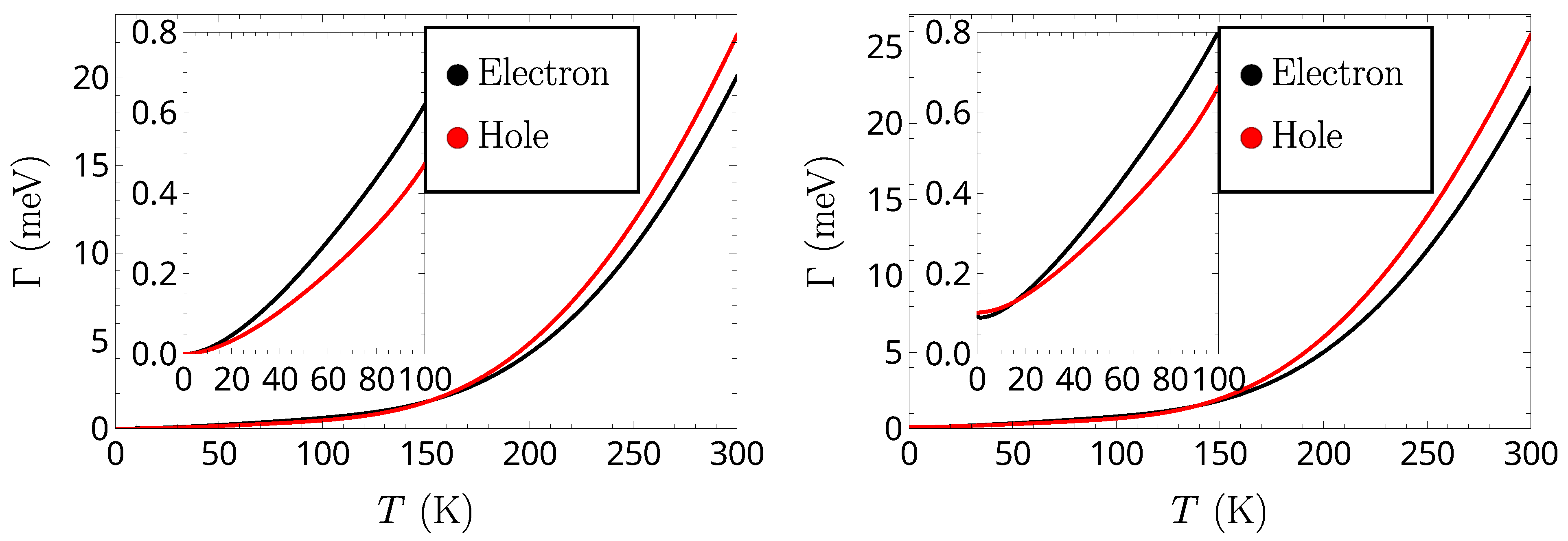
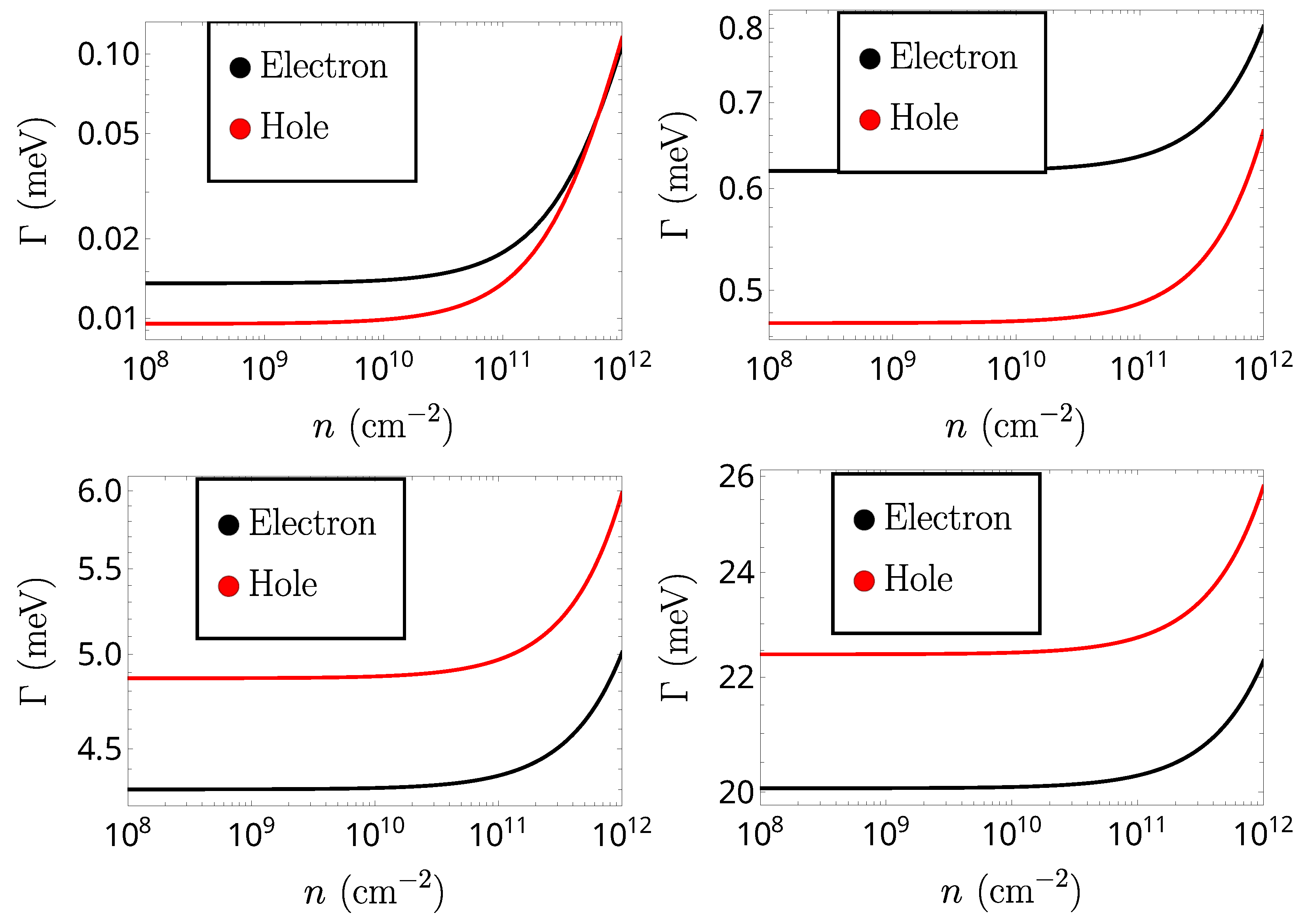
4. Scattering Contribution to Exciton Linewidth

To conclude our study of the scattering of excitons with free carriers in layered materials, we will now discuss the contribution from these scattering processes to the excitonic linewidth. This will provide a point of comparison against experimental studies [54]. Although other phenomena will also contribute to this linewidth, such as radiative lifetimes [27] and phonon scattering [25], the dependence of the free carrier scattering on both temperature and carrier density should provide a good distinction of the various contributing processes. As hBN is a large bandgap insulator, carrier doping in this material is usually performed chemically by diluting impurities [55,56,57,58].
The contribution to the excitonic linewidth from free carrier scattering is given by [24,59,60,61]
Γ Total = f 2 2 π M 0 d k k 2 f m c + m e + m h m e + m h k Q 1 s f ,
where Q 1 s f is, as described earlier, the scattering cross section associated with a specific transition from the excitonic ground state to a final state f. As we are summing over final states f, and only Q 1 s f depends on the final state, this is equivalent to switching the sum over final states and the integral and writing
Γ Total = 2 2 π M 0 d k k 2 n F m c + m e + m h m e + m h k Q Total ,
where Q Total is the total scattering cross section as plotted in Figure 3. Here, n F ( k ) is the Fermi–Dirac distribution for free carriers, given by
n F ( k ) = 1 e E k E F k B T + 1
where the dispersion relation is given by
E k = 2 2 m c k 2
and the Fermi energy is
E F = 2 π 2 2 m c n ,
with n the area density of free carriers. We consider carrier densities up to a maximum of 10 12 cm 2 , where the average separation of free carriers d c = 2 ( π n ) 1 / 2 is still larger but already of the order of the root mean square (RMS) exciton radius, given by
r RMS ; n = 0 0 2 π r d r d θ ψ n ( r , θ ) r 2 ψ n ( r , θ ) .
For the two excitonic states most relevant to the scattering cross section, 1 s and 2 p , the RMS exciton radius is r RMS ; 1 s = 19.5 Å and r RMS ; 2 p = 73.2 Å , respectively, while the average separation between free carriers is d c = 113 Å .
As before, we must compute the integral of Equation (30) numerically. The specific methodology for the discretization of Equation (30) is discussed in Appendix B. Choosing a Gauss–Legendre quadrature [62] of size N = 450 , the results for the contribution of scattering with free carriers to the excitonic linewidth are presented in Figure 4 as a function of temperature for free carrier area densities of n = 10 9 cm 2 and n = 10 12 cm 2 . In Figure 5, we present the excitonic linewidth as a function of the free carrier area density for four distinct values of the temperature T between 10 K and 300 K . As expected, the excitonic linewidth contribution increases with both temperature and carrier density as these phenomena increase the kinetic energy of the carriers and their proximity, respectively.

5. Conclusions

In this paper, we studied the effects of scattering between free carriers and excitons in monolayer materials and its contribution to the excitonic linewidth. To this end, we began by reviewing the general form of the expressions for the differential cross section between free carriers and excitons in two dimensions [37], as well as the inclusion of screening in the differential cross section. Briefly reviewing the computation of variational functions for the exciton wave functions, we discussed both elastic and inelastic scattering processes.
While elastic scattering was the sole contributor to the scattering cross section for low relative momentum, inelastic 1 s 2 p scattering dominated the total cross section when allowed by conservation of energy. This dominant scattering had a maximum cross section roughly 40 times larger than that of elastic scattering, as seen in Figure 3. Considering inelastic scattering processes to higher energy states, namely 2 s and 3 d , their amplitude was negligible when compared to the dominant process (roughly 400 times smaller). This dominant behavior of 1 s 2 p transitions was very similar to what was presented in Figures 2 and 9 of Ref. [37], although the specific ratios were highly dependent on the electron and hole masses.
After discussing the relation between the total scattering cross section and the excitonic linewidth, we considered its dependence on both temperature and free carrier density. First, looking at the exciton linewidth for reasonable values of the carrier density in layered materials [63,64,65], namely 10 9 cm 2 and 10 12 cm 2 , we observed that the difference in linewidth between the two regimes was clearly noticeable as the linewidth became finite at T = 0 K for larger carrier densities. Additionally, the contribution from exciton–hole scattering became larger than that of electron–exciton scattering slightly earlier at a higher carrier density, namely at T 150 K for n = 10 9 cm 2 and at T 140 K for n = 10 12 cm 2 . Further increasing the carrier density to values above 10 13 cm 2 would produce even greater differences. These higher carrier densities would already imply an average free carrier separation d c much smaller than the RMS exciton radius for the 2 p excitonic state, which would make more complex excitonic phenomena, such as biexcitons and trions [66,67,68,69], increasingly significant.
Regarding the excitonic linewidth at fixed temperatures, the free carrier scattering contribution remained in the 0.5–20 meV range for temperatures between 100 and 300 K. For temperatures in this range, the computed linewidth remained essentially constant at a temperature-dependent value as the carrier density increased until roughly n 10 11 cm 2 . Past n 10 11 cm 2 , the computed linewidth rapidly increased for all values of the temperature, although the growth occurred sooner and faster for lower temperatures, as can be seen in the top-left plot of Figure 5 for T = 10 K .
From these results, it should be feasible to measure the free-carrier scattering contribution to the excitonic linewidth, as good quality samples of both hBN and transition metal dichalcogenides have been grown in the past that presented excitonic linewidths in this order of magnitude [11,12,13,14,15].

Author Contributions

Formal analysis, M.F.C.M.Q.; Supervision, N.M.R.P.; Writing—original draft, M.F.C.M.Q.; Writing—review & editing, N.M.R.P. All authors have read and agreed to the published version of the manuscript.

Funding

M.F.C.M.Q. acknowledges the International Nanotechnology Laboratory (INL) and the Portuguese Foundation for Science and Technology (FCT) for the Quantum Portugal Initiative (QPI) grant SFRH/BD/151114/2021. N.M.R.P. acknowledges support by the Portuguese Foundation for Science and Technology (FCT) in the framework of the Strategic Funding UIDB/04650/2020, COMPETE 2020, PORTUGAL 2020, FEDER, and FCT through projects PTDC/FIS-MAC/2045/2021, EXPL/FIS-MAC/0953/ 2021, and from the European Commission through the project Graphene Driven Revolutions in ICT and Beyond (Ref. No. 881603, CORE 3).

Institutional Review Board Statement

Not applicable.

Informed Consent Statement

Not applicable.

Data Availability Statement

Not applicable.

Conflicts of Interest

The authors declare no conflict of interest.

Abbreviations

The following abbreviations are used in this manuscript:
hBNhexagonal boron nitride
RMSroot mean squared

Appendix A. Derivation of Differential Scattering Cross Section

For the derivation of the differential scattering cross section of Equation (2), we follow closely the derivation performed by Feng and Spector [41]. We consider an encounter between two bodies A (free carrier) and B (exciton), which are in their ground state prior to the collision. The reduced mass of this system is M = m A m B m A + m B . Prior to the collision, the internal motions of each of the two bodies are given by their independent Hamiltonians
H A χ A , n r A = E A , n χ A , n r A , H B χ B , m r B = E B , m χ B , m r B ,
where χ A , n / χ B , m are the independent wave functions for the internal motion of the two bodies A / B in the states n / m , respectively, and E A , n / E B , m their energies. In the absence of the interaction of the two bodies, their relative motion is given by
2 2 M 2 1 2 M v 2 F 11 ( R ) = 0 ,
with v and R the relative velocity and position of the two particles and F 11 ( R ) the part of the wave function related to the relative motion of the particles in their ground state.
The complete wave equation for this system is given by
2 2 M 2 1 2 M v 2 + H A E A , 1 + H B E B , 1 + V R , r A , r B Ψ R , r A , r B = 0 ,
where V R , r A , r B is the interaction potential between the two particles. The wave function can then be expanded in terms of the basis functions χ A , n / χ B , m , reading
Ψ R , r A , r B = n , m F n m ( R ) χ A , n r A χ B , m r B ,
meaning that F n m ( R ) must obey
2 + k 2 F n m ( R ) = 2 M 2 d r A d r B V r A , r B , R Ψ r A , r B , R χ A n * r A χ B m * r B ,
where
k 2 = 2 M 2 1 2 M v 2 + E A , 1 E A , n + E B , 1 E B , m .
The relation in Equation (A6) immediately leads to the thresholds for inelastic scattering, as k being real implies 1 2 M v 2 > E A , n E A , 1 + E B , m E B , 1 .
The solution to Equation (A5) reads
F n m ( R ) = i M 2 2 d r A d r B d R V r A , r B , R Ψ R , r A , r B χ A , n * r A χ B , m * r B H 0 1 k R R ,
where H 0 1 k R R is the Hankel function of the first kind, which is the solution to Equation (A2). This function satisfies the boundary condition that, for R R , the solution represents an outgoing circular wave.
Following an identical procedure to that which is used to apply the Born approximation in a 3D system, the asymptotic regime as R for F n m ( R ) reads
F n m ( R ) e i k 0 · R + e i k · R R f n m ( θ ) ,
where it was assumed that the asymptotic form of the solution is the sum of an incoming plane wave and an outgoing circular wave. In Equation (A8), k 0 / k are the initial/final wave vectors for the scattered particles, respectively, and
f n m ( θ ) = M e i π / 4 2 π k 2 d r A d r B d R e i k 0 k · R V r A , r B , R χ A , n * r A χ A , 1 r A χ B , m * r B χ B , 1 r B .
The 2D differential scattering cross section is, analogously to that of a 3D system, given by [41]
I n , m ( θ ) = k k 0 f n m ( θ ) 2 = M 2 2 π k 0 4 d r A d r B d R e i q · R V r A , r B , R χ A , n * r A χ A , 1 r A χ B , m * r B χ B , 1 r B 2 ,
with q = k 0 k . Finally, recalling that the free carrier (electron or hole) has no internal structure, the sum of the internal energies of the system reduces to that of the exciton. Furthermore, Equation (A10) can be simplified further by assuming a central field approximation, reading
I n , m ( θ ) = M 2 2 π k 0 4 d r d R e i q · R V r , R χ n * r χ 1 r 2 ,
where χ is now the wave function of the exciton, r is the relative position of the electron and hole in the exciton, and R is the relative position from the free carrier to the center of mass of the exciton.

Appendix B. Computation of Scattering Contribution to Excitonic Linewidth

We begin by changing the integration limits 0 , + to a finite limit, in this case 0 , 1 , via a change in variables defined as k = tan π x 2 . With this change in variables, the integral of Equation (30) reads
Γ Total = 2 2 π M 0 1 d x d k d x k ( x ) 2 n F m c + m e + m h m e + m h k ( x ) Q Total ( k ( x ) ) .
We can then define a grid of points x i for our discretization, meaning that
Γ Total = 2 2 π M i = 1 N w i d k d x i k i 2 n F m c + m e + m h m e + m h k i Q Total ( k i ) ,
where N is the number of points considered in the discretization, w i is the weight function of the quadrature in question, and the discretized variables are defined as q i q x i , and d k d x i d k d x x = x i . For the numerical quadrature, we employ a Gauss–Legendre quadrature [62], defined as
a b f x d x i = 1 N f x i w i ,
where
x i = a + b + b a ξ i 2 ,       w i = b a 1 ξ i 2 d P N x d x x = ξ i 2 ,
with ξ i the i-th zero of the Legendre polynomial P N x .

References

  1. Àla Guillaume, C.B.; Debever, J.M.; Salvan, F. Radiative Recombination in Highly Excited CdS. Phys. Rev. 1969, 177, 567–580. [Google Scholar] [CrossRef]
  2. Iwai, S.; Namba, S. Emission Spectra in CdS under High Excitation by Electron Beam. Appl. Phys. Lett. 1971, 19, 41–43. [Google Scholar] [CrossRef]
  3. In Yu, C.; Goto, T.; Ueta, M. Emission of Cuprous Halide Crystals at High Density Excitation. J. Phys. Soc. Jpn. 1973, 34, 693–698. [Google Scholar] [CrossRef]
  4. Braun, W.; Bille, J.; Fischer, T.; Huber, G. Laser Emission in CdSe Due to Exciton—Exciton and Exciton—Electron Interaction. Phys. Status Solidi (B) 1973, 58, 759–765. [Google Scholar] [CrossRef]
  5. Levy, R.; Grun, J.B. Optical properties of strongly excited direct band gap materials. Phys. Status Solidi (A) 1974, 22, 11–38. [Google Scholar] [CrossRef]
  6. Klingshirn, C. The Luminescence of ZnO under High One- and Two-Quantum Excitation. Phys. Status Solidi (B) 1975, 71, 547–556. [Google Scholar] [CrossRef]
  7. Hönerlage, B.; Klingshirn, C.; Grun, J.B. Spontaneous emission due to exciton—Electron scattering in semiconductors. Phys. Status Solidi (B) 1976, 78, 599–608. [Google Scholar] [CrossRef]
  8. Levy, R.; Grun, J.B.; Nikitine, S. Experimental investigation of the competition of stimulated emissions involving exciton. Excit. High Density 1975, 73, 211–219. [Google Scholar]
  9. Elkomoss, S.G.; Munschy, G. Electron-exciton elastic scattering cross sections in the central field and the exchange approximations. J. Phys. Chem. Solids 1977, 38, 557–563. [Google Scholar] [CrossRef]
  10. Elkomoss, S.G.; Munschy, G. Electron-exciton inelastic collision cross sections for different semiconductors. J. Phys. Chem. Solids 1979, 40, 431–438. [Google Scholar] [CrossRef]
  11. Reynolds, D.C.; Bajaj, K.K.; Litton, C.W.; Singh, J.; Yu, P.W.; Pearah, P.; Klem, J.; Morkoc, H. High-resolution photoluminescence and reflection studies of GaAs-AlxGa1−xAs multi-quantum-well structures grown by molecular-beam epitaxy: Determination of microscopic structural quality of interfaces. Phys. Rev. B 1986, 33, 5931–5934. [Google Scholar] [CrossRef] [PubMed]
  12. Museur, L.; Feldbach, E.; Kanaev, A. Defect-related photoluminescence of hexagonal boron nitride. Phys. Rev. B 2008, 78, 155204. [Google Scholar] [CrossRef] [Green Version]
  13. Cadiz, F.; Courtade, E.; Robert, C.; Wang, G.; Shen, Y.; Cai, H.; Taniguchi, T.; Watanabe, K.; Carrere, H.; Lagarde, D.; et al. Excitonic Linewidth Approaching the Homogeneous Limit in MoS2-Based van der Waals Heterostructures. Phys. Rev. X 2017, 7, 021026. [Google Scholar] [CrossRef] [Green Version]
  14. Elias, C.; Valvin, P.; Pelini, T.; Summerfield, A.; Mellor, C.J.; Cheng, T.S.; Eaves, L.; Foxon, C.T.; Beton, P.H.; Novikov, S.V.; et al. Direct band-gap crossover in epitaxial monolayer boron nitride. Nat. Commun. 2019, 10, 2639. [Google Scholar] [CrossRef] [PubMed] [Green Version]
  15. Li, J.; Wang, J.; Zhang, X.; Elias, C.; Ye, G.; Evans, D.; Eda, G.; Redwing, J.M.; Cassabois, G.; Gil, B.; et al. Hexagonal Boron Nitride Crystal Growth from Iron, a Single Component Flux. ACS Nano 2021, 15, 7032–7039. [Google Scholar] [CrossRef]
  16. Vuong, T.Q.P.; Cassabois, G.; Valvin, P.; Rousseau, E.; Summerfield, A.; Mellor, C.J.; Cho, Y.; Cheng, T.S.; Albar, J.D.; Eaves, L.; et al. Deep ultraviolet emission in hexagonal boron nitride grown by high-temperature molecular beam epitaxy. 2D Materials 2017, 4, 021023. [Google Scholar] [CrossRef]
  17. Kim, S.M.; Hsu, A.; Park, M.H.; Chae, S.H.; Yun, S.J.; Lee, J.S.; Cho, D.H.; Fang, W.; Lee, C.; Palacios, T.; et al. Synthesis of large-area multilayer hexagonal boron nitride for high material performance. Nat. Commun. 2015, 6, 8662. [Google Scholar] [CrossRef] [Green Version]
  18. Yano, M.; Yap, Y.K.; Okamoto, M.; Onda, M.; Yoshimura, M.; Mori, Y.; Sasaki, T. Na: A New Flux for Growing Hexagonal Boron Nitride Crystals at Low Temperature. Jpn. J. Appl. Phys. 2000, 39, L300–L302. [Google Scholar] [CrossRef]
  19. Dingle, R.; Wiegmann, W.; Henry, C.H. Quantum States of Confined Carriers in Very Thin AlxGa1−xAs-GaAs-AlxGa1−xAs Heterostructures. Phys. Rev. Lett. 1974, 33, 827–830. [Google Scholar] [CrossRef]
  20. Miller, D.A.B.; Chemla, D.S.; Eilenberger, D.J.; Smith, P.W.; Gossard, A.C.; Tsang, W.T. Large room-temperature optical nonlinearity in GaAs/Ga1−xAlxAs multiple quantum well structures. Appl. Phys. Lett. 1982, 41, 679–681. [Google Scholar] [CrossRef]
  21. Poellmann, C.; Steinleitner, P.; Leierseder, U.; Nagler, P.; Plechinger, G.; Porer, M.; Bratschitsch, R.; Schüller, C.; Korn, T.; Huber, R. Resonant internal quantum transitions and femtosecond radiative decay of excitons in monolayer WSe2. Nat. Mater. 2015, 14, 889–893. [Google Scholar] [CrossRef]
  22. Merkl, P.; Mooshammer, F.; Steinleitner, P.; Girnghuber, A.; Lin, K.Q.; Nagler, P.; Holler, J.; Schüller, C.; Lupton, J.M.; Korn, T.; et al. Ultrafast transition between exciton phases in van der Waals heterostructures. Nat. Mater. 2019, 18, 691–696. [Google Scholar] [CrossRef] [PubMed] [Green Version]
  23. Lee, J.; Koteles, E.S.; Vassell, M.O. Luminescence linewidths of excitons in GaAs quantum wells below 150 K. Phys. Rev. B 1986, 33, 5512–5516. [Google Scholar] [CrossRef] [PubMed]
  24. Spector, H.N.; Lee, J.; Melman, P. Exciton linewidth in semiconducting quantum-well structures. Phys. Rev. B 1986, 34, 2554–2560. [Google Scholar] [CrossRef]
  25. Henriques, J.C.G.; Mortensen, N.A.; Peres, N.M.R. Analytical description of the 1s exciton linewidth temperature dependence in transition metal dichalcogenides. Phys. Rev. B 2021, 103, 235402. [Google Scholar] [CrossRef]
  26. Cingolani, R.; Ploog, K. Frequency and density dependent radiative recombination processes in III–V semiconductor quantum wells and superlattices. Adv. Phys. 1991, 40, 535–623. [Google Scholar] [CrossRef]
  27. Palummo, M.; Bernardi, M.; Grossman, J.C. Exciton Radiative Lifetimes in Two-Dimensional Transition Metal Dichalcogenides. Nano Lett. 2015, 15, 2794–2800. [Google Scholar] [CrossRef] [Green Version]
  28. Singh, J.; Bajaj, K.K. Theory of excitonic photoluminescence linewidth in semiconductor alloys. Appl. Phys. Lett. 1984, 44, 1075–1077. [Google Scholar] [CrossRef]
  29. Basu, P.K. Linewidth of free excitons in quantum wells: Contribution by alloy disorder scattering. Appl. Phys. Lett. 1990, 56, 1110–1112. [Google Scholar] [CrossRef]
  30. Li, W.; Wang, Z.; Song, A.; Liang, J.; Xu, B.; Zhu, Z.; Zheng, W.; Liao, Q.; Yang, B. Photoluminescence studies on very high-density quasi-two-dimensional electron gases in pseudomorphic modulation-doped quantum wells. J. Appl. Phys. 1995, 78, 593–595. [Google Scholar] [CrossRef]
  31. Djurišić, A.B.; Kwok, W.M.; Leung, Y.H.; Chan, W.K.; Phillips, D.L.; Lin, M.S.; Gwo, S. Ultrafast spectroscopy of stimulated emission in single ZnO tetrapod nanowires. Nanotechnology 2005, 17, 244–249. [Google Scholar] [CrossRef]
  32. Young, J.F.; Wood, B.M.; Charbonneau, S. Optical Probes of Resonant Tunneling Structures. In Electronic Properties of Multilayers and Low-Dimensional Semiconductor Structures; Springer: Boston, MA, USA, 1990; pp. 331–349. [Google Scholar] [CrossRef]
  33. Teran, F.J.; Martín, M.D.; Calleja, J.M.; Viña, L.; Eaves, L.; Henini, M. Carrier injection effects on exciton dynamics in GaAs/AlAs resonant-tunneling diodes. EPL (Europhys. Lett.) 2009, 85, 67010. [Google Scholar] [CrossRef]
  34. Koh, T.S.; Feng, Y.P.; Spector, H.N. Effect of an electric field on the scattering of excitons by free carriers in semiconducting quantum-well structures. J. Appl. Phys. 1997, 81, 2704–2708. [Google Scholar] [CrossRef]
  35. Vella, D.; Barbosa, M.B.; Trevisanutto, P.E.; Verzhbitskiy, I.; Zhou, J.Y.; Watanabe, K.; Taniguchi, T.; Kajikawa, K.; Eda, G. In-Plane Field-Driven Excitonic Electro-Optic Modulation in Monolayer Semiconductor. Adv. Opt. Mater. 2022, 10, 2102132. [Google Scholar] [CrossRef]
  36. Efimkin, D.K.; Laird, E.K.; Levinsen, J.; Parish, M.M.; MacDonald, A.H. Electron-exciton interactions in the exciton-polaron problem. Phys. Rev. B 2021, 103, 075417. [Google Scholar] [CrossRef]
  37. Feng, Y.P.; Spector, H.N. Scattering of excitons by free carriers in semiconducting quantum well structures. J. Phys. Chem. Solids 1987, 48, 593–601. [Google Scholar] [CrossRef]
  38. Massey, H.S.W.; Moiseiwitsch, B.L. The application of variational methods to atomic scattering problems—I. The elastic scattering of electrons by hydrogen atoms. Proc. R. Soc. Lond. Ser. A Math. Phys. Sci. 1951, 205, 483–496. [Google Scholar] [CrossRef]
  39. Bates, D.R.; Griffing, G. Inelastic Collisions between Heavy Particles I: Excitation and Ionization of Hydrogen Atoms in Fast Encounters with Protons and with other Hydrogen Atoms. Proc. Phys. Soc. Sect. A 1953, 66, 961–971. [Google Scholar] [CrossRef]
  40. Mott, N.F.; Massey, H.S.W. Theory of Atomic Collisions, 3rd ed.; Monographs on Physics; Oxford University Press: London, UK, 1965. [Google Scholar]
  41. Feng, Y.P.; Spector, H. Scattering of screened excitons by free carriers in semiconducting quantum well structures. IEEE J. Quantum Electron. 1988, 24, 1659–1663. [Google Scholar] [CrossRef]
  42. Rytova, S.N. The Screened Potential of a Point Charge in a Thin Film. arXiv 2018, arXiv:1806.00976. [Google Scholar]
  43. Keldysh, L.V. Coulomb interaction in thin semiconductor and semimetal films. Sov. J. Exp. Theor. Phys. Lett. 1979, 29, 658. [Google Scholar]
  44. Li, P.; Appelbaum, I. Excitons without effective mass: Biased bilayer graphene. Phys. Rev. B 2019, 99, 035429. [Google Scholar] [CrossRef] [Green Version]
  45. Versteegh, M.A.M.; Kuis, T.; Stoof, H.T.C.; Dijkhuis, J.I. Ultrafast screening and carrier dynamics in ZnO: Theory and experiment. Phys. Rev. B 2011, 84, 035207. [Google Scholar] [CrossRef] [Green Version]
  46. Quintela, M.F.C.M.; Henriques, J.C.G.; Tenório, L.G.M.; Peres, N.M.R. Theoretical Methods for Excitonic Physics in 2D Materials. Phys. Status Solidi (B) 2022, 259, 2200097. [Google Scholar] [CrossRef]
  47. Gomes, J.N.S.; Trallero-Giner, C.; Vasilevskiy, M.I. Variational calculation of the lowest exciton states in phosphorene and transition metal dichalcogenides. J. Phys. Condens. Matter 2021, 34, 045702. [Google Scholar] [CrossRef]
  48. Lee, Y.C.; Lin, D.L. Wannier excitons in a thin crystal film. Phys. Rev. B 1979, 19, 1982–1989. [Google Scholar] [CrossRef]
  49. Yang, X.L.; Guo, S.H.; Chan, F.T.; Wong, K.W.; Ching, W.Y. Analytic solution of a two-dimensional hydrogen atom. I. Nonrelativistic theory. Phys. Rev. A 1991, 43, 1186–1196. [Google Scholar] [CrossRef]
  50. Wannier, G.H. The Structure of Electronic Excitation Levels in Insulating Crystals. Phys. Rev. 1937, 52, 191–197. [Google Scholar] [CrossRef]
  51. Serway, R.A.; Faughn, J.S.; Moses, C.J. College Physics; Number Volume 1 in College Physics; Brooks/Cole: Devon, UK, 2003. [Google Scholar]
  52. Ferreira, F.; Chaves, A.J.; Peres, N.M.R.; Ribeiro, R.M. Excitons in hexagonal boron nitride single-layer: A new platform for polaritonics in the ultraviolet. J. Opt. Soc. Am. B 2019, 36, 674–683. [Google Scholar] [CrossRef] [Green Version]
  53. Henriques, J.C.G.; Ventura, G.B.; Fernandes, C.D.M.; Peres, N.M.R. Optical absorption of single-layer hexagonal boron nitride in the ultraviolet. J. Phys. Cond. Matter 2020, 32, 025304. [Google Scholar] [CrossRef] [Green Version]
  54. Selig, M.; Berghäuser, G.; Raja, A.; Nagler, P.; Schüller, C.; Heinz, T.F.; Korn, T.; Chernikov, A.; Malic, E.; Knorr, A. Excitonic linewidth and coherence lifetime in monolayer transition metal dichalcogenides. Nat. Commun. 2016, 7, 13279. [Google Scholar] [CrossRef]
  55. Zhang, Z.; Guo, W. Controlling the Functionalizations of Hexagonal Boron Nitride Structures by Carrier Doping. J. Phys. Chem. Lett. 2011, 2, 2168–2173. [Google Scholar] [CrossRef]
  56. Majety, S.; Doan, T.C.; Li, J.; Lin, J.Y.; Jiang, H.X. Electrical transport properties of Si-doped hexagonal boron nitride epilayers. AIP Adv. 2013, 3, 122116. [Google Scholar] [CrossRef]
  57. He, B.; Qiu, M.; Yuen, M.F.; Zhang, W.J. Electrical properties and electronic structure of Si-implanted hexagonal boron nitride films. Appl. Phys. Lett. 2014, 105, 012104. [Google Scholar] [CrossRef]
  58. Sun, F.; Hao, Z.; Liu, G.; Wu, C.; Lu, S.; Huang, S.; Liu, C.; Hong, Q.; Chen, X.; Cai, D.; et al. p-Type conductivity of hexagonal boron nitride as a dielectrically tunable monolayer: Modulation doping with magnesium. Nanoscale 2018, 10, 4361–4369. [Google Scholar] [CrossRef]
  59. Feng, Y.P.; Spector, H.N. Exciton linewidth due to scattering from free carriers in semiconducting quantum well structures. Superlattices Microstruct. 1987, 3, 459–461. [Google Scholar] [CrossRef]
  60. Feng, Y.P. Excitons in Semiconducting Quantum Well Structures. Ph.D. Thesis, Illinois Institute of Technology, Chicago, IL, USA, 1989. [Google Scholar]
  61. Koh, T.S.; Feng, Y.P.; Spector, H.N. Exciton linewidth due to scattering by free carriers in semiconducting quantum well structures: Finite confining potential model. J. Appl. Phys. 1997, 81, 2236–2240. [Google Scholar] [CrossRef]
  62. Kythe, P.K.; Puri, P. Computational Methods for Linear Integral Equations; Birkhäuser: Boston, MA, USA, 2002. [Google Scholar]
  63. Du, Y.; Neal, A.T.; Zhou, H.; Ye, P.D. Transport studies in 2D transition metal dichalcogenides and black phosphorus. J. Phys. Condens. Matter 2016, 28, 263002. [Google Scholar] [CrossRef] [Green Version]
  64. Kuiri, M.; Srivastav, S.K.; Ray, S.; Watanabe, K.; Taniguchi, T.; Das, T.; Das, A. Enhanced electron-phonon coupling in doubly aligned hexagonal boron nitride bilayer graphene heterostructure. Phys. Rev. B 2021, 103, 115419. [Google Scholar] [CrossRef]
  65. Li, J.; Goryca, M.; Yumigeta, K.; Li, H.; Tongay, S.; Crooker, S.A. Valley relaxation of resident electrons and holes in a monolayer semiconductor: Dependence on carrier density and the role of substrate-induced disorder. Phys. Rev. Mater. 2021, 5, 044001. [Google Scholar] [CrossRef]
  66. Lampert, M.A. Mobile and Immobile Effective-Mass-Particle Complexes in Nonmetallic Solids. Phys. Rev. Lett. 1958, 1, 450–453. [Google Scholar] [CrossRef]
  67. Kheng, K.; Cox, R.T.; d’Aubigné, M.Y.; Bassani, F.; Saminadayar, K.; Tatarenko, S. Observation of negatively charged excitons X in semiconductor quantum wells. Phys. Rev. Lett. 1993, 71, 1752–1755. [Google Scholar] [CrossRef]
  68. Chen, G.; Stievater, T.H.; Batteh, E.T.; Li, X.; Steel, D.G.; Gammon, D.; Katzer, D.S.; Park, D.; Sham, L.J. Biexciton Quantum Coherence in a Single Quantum Dot. Phys. Rev. Lett. 2002, 88, 117901. [Google Scholar] [CrossRef]
  69. Li, X.; Wu, Y.; Steel, D.; Gammon, D.; Stievater, T.H.; Katzer, D.S.; Park, D.; Piermarocchi, C.; Sham, L.J. An All-Optical Quantum Gate in a Semiconductor Quantum Dot. Science 2003, 301, 809–811. [Google Scholar] [CrossRef] [Green Version]
Figure 1. Total elastic cross section for electron–exciton (black) and hole–exciton (red) scattering in hBN encapsulated in fused quartz as a function of the initial relative wave vector.
Applsci 12 07872 g001
Figure 2. Radial probability density for the 1 s (blue), 2 s (orange), and 2 p (green) states as described by the variational wave functions of Equations (14) and (23) in a hBN monolayer encapsulated in fused quartz.
Applsci 12 07872 g002
Figure 3. Total cross section for electron–exciton (black) and hole–exciton (red) scattering in hBN encapsulated in fused quartz as a function of the initial relative wave vector. Vertical dashed lines represent the electron–exciton and hole–exciton scattering thresholds for the 1 s 2 p transition, located at k min , e = 0.0822 Å 1 and k min , h = 0.0749 Å 1 .
Applsci 12 07872 g003
Figure 4. Contribution to exciton linewidth from scattering with free carriers as a function of the temperature at constant free carrier area density n = 10 9 cm 2 (left) and n = 10 12 cm 2 (right). Insets show the low–temperature region of the plot for clarity.
Applsci 12 07872 g004
Figure 5. Contribution to exciton linewidth from scattering with free carriers as a function of the free carrier area density at constant temperature T = 10 K (top-left), T = 100 K (top-right), T = 200 K (bottom-left), and T = 300 K (bottom-right).
Applsci 12 07872 g005
Publisher’s Note: MDPI stays neutral with regard to jurisdictional claims in published maps and institutional affiliations.

