
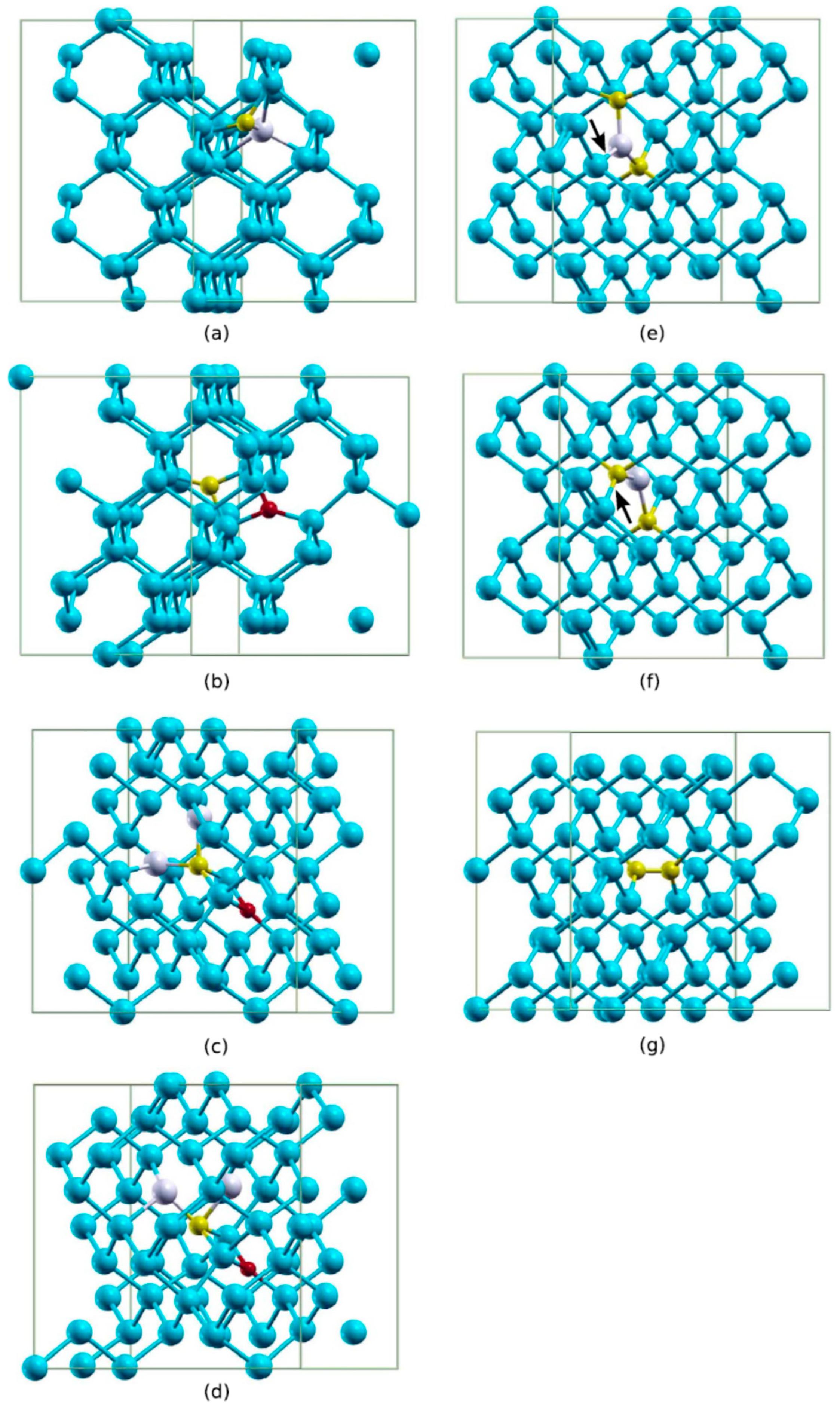
Comparative Study of Oxygen- and Carbon-Related Defects in Electron Irradiated Cz–Si Doped with Isovalent Impurities


 ,
,
Abstract
:1. Introduction
2. Results
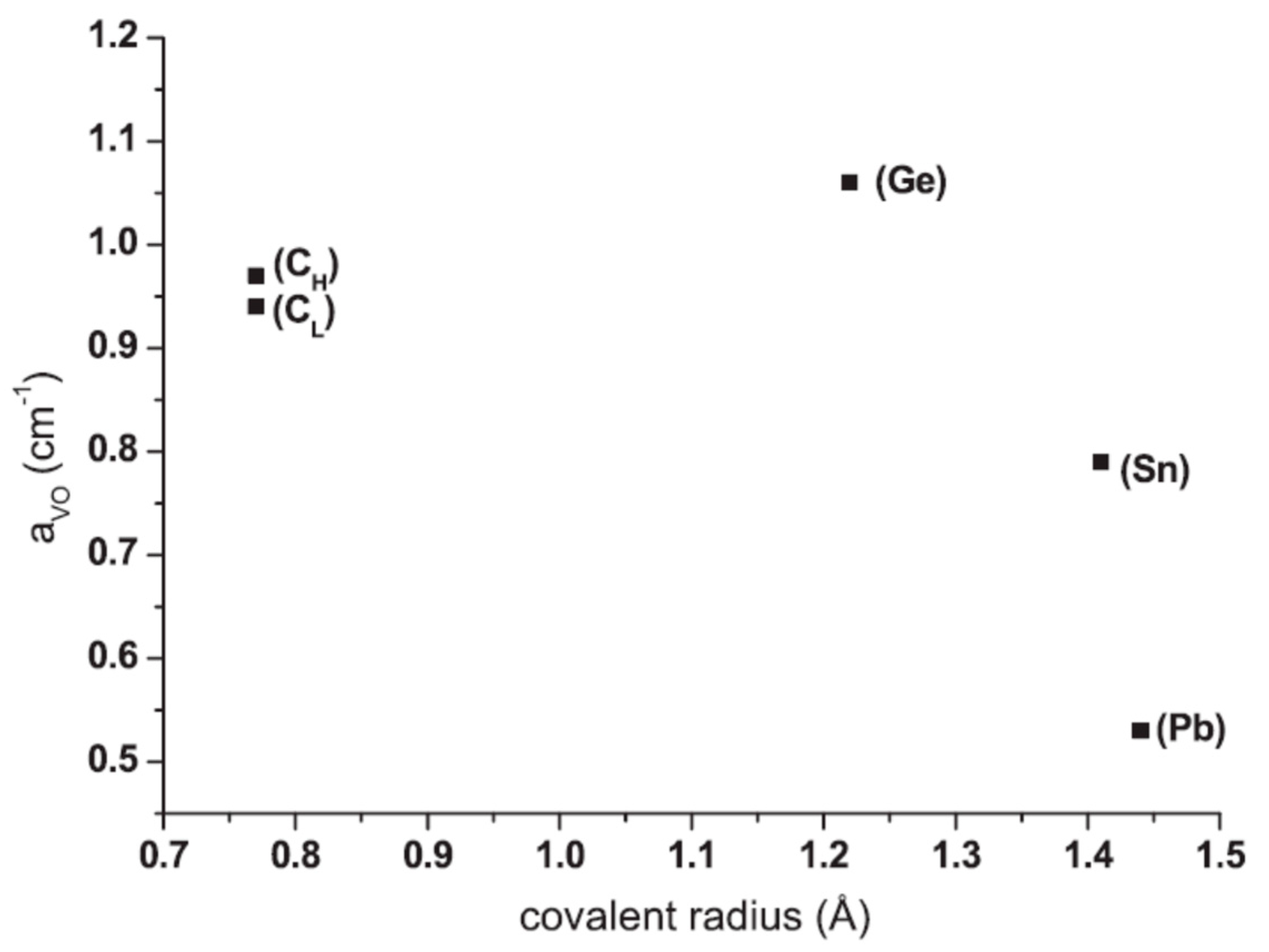
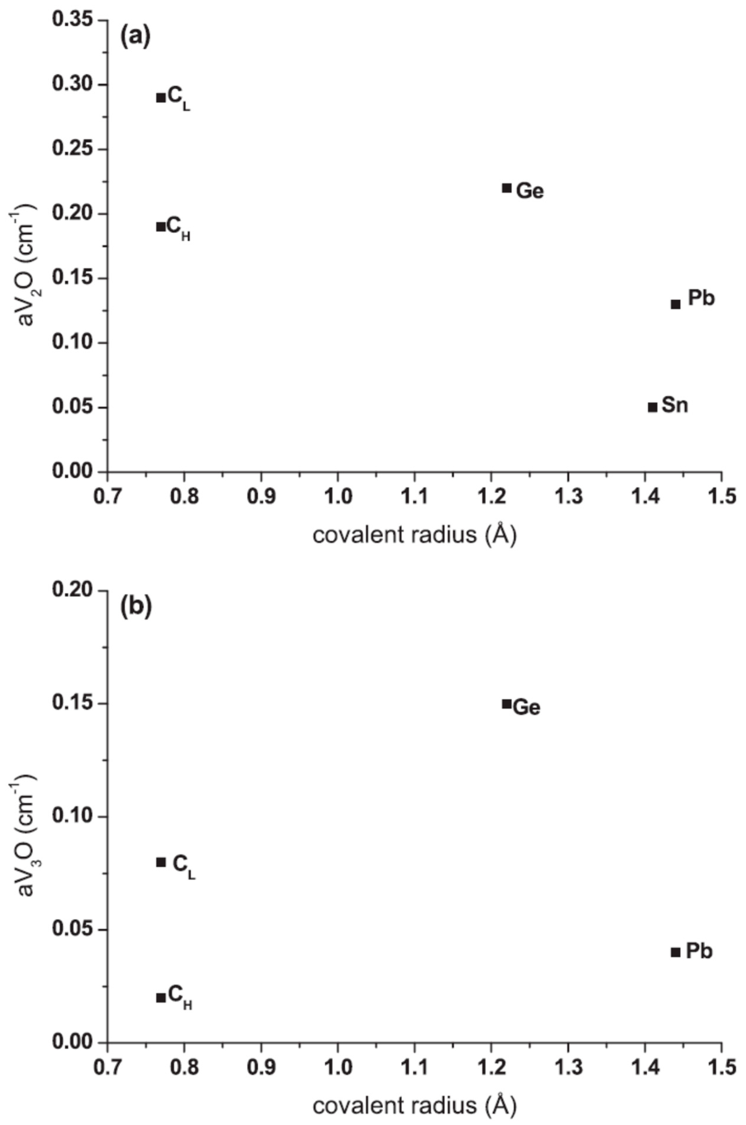
2.1. Production of VO Defect as a Function of the Isovalent Dopant Covalent Radius
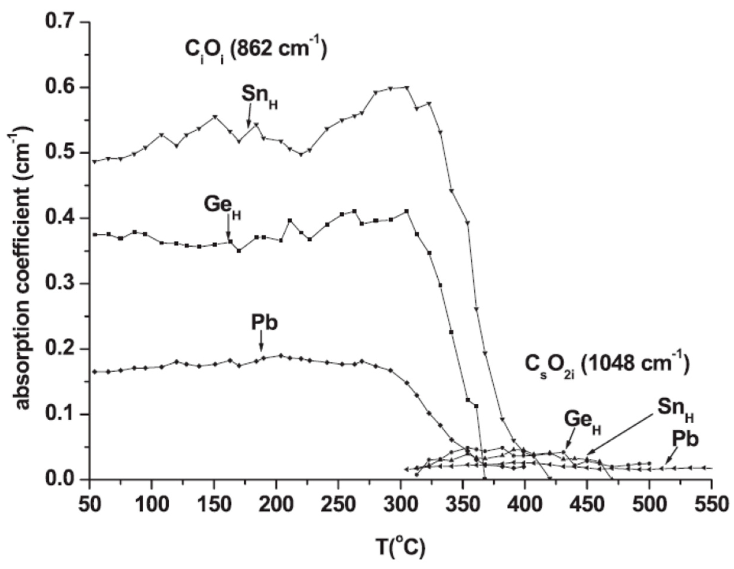
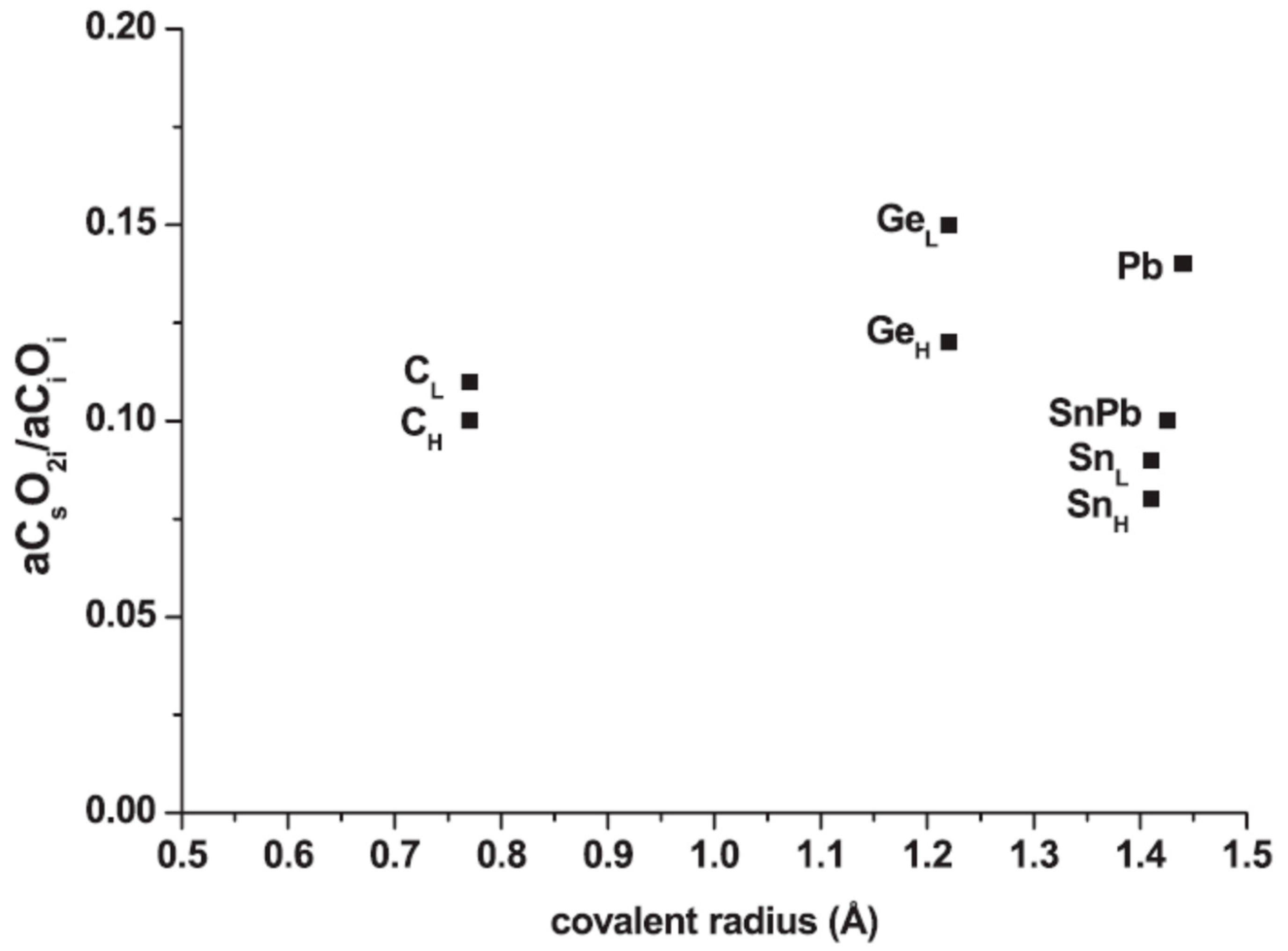
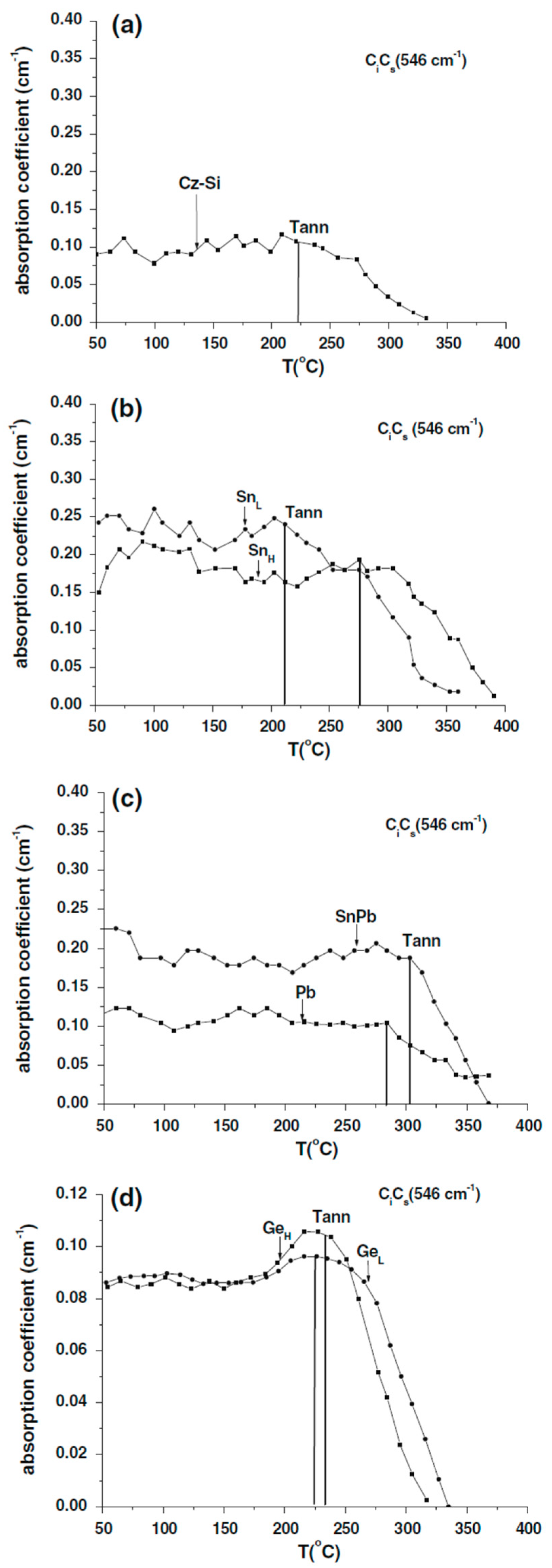
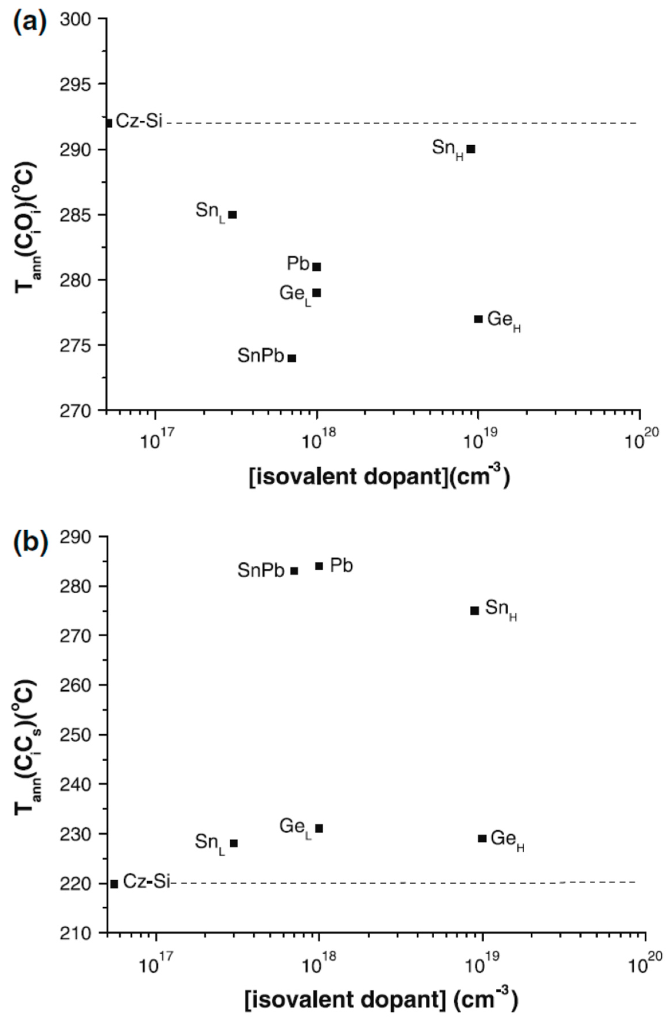
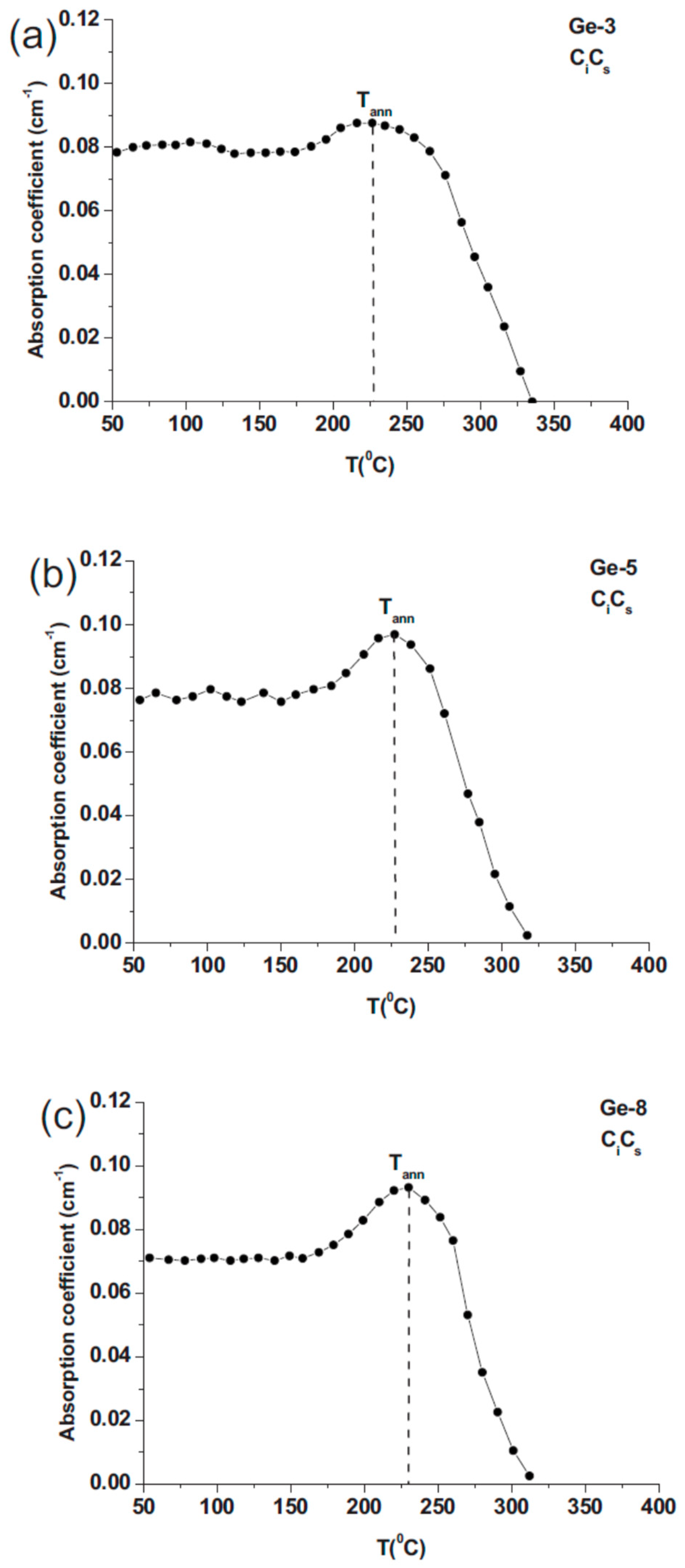
2.2. Conversion of VO to VO2 Defect Versus Isovalent Dopant Covalent Radius
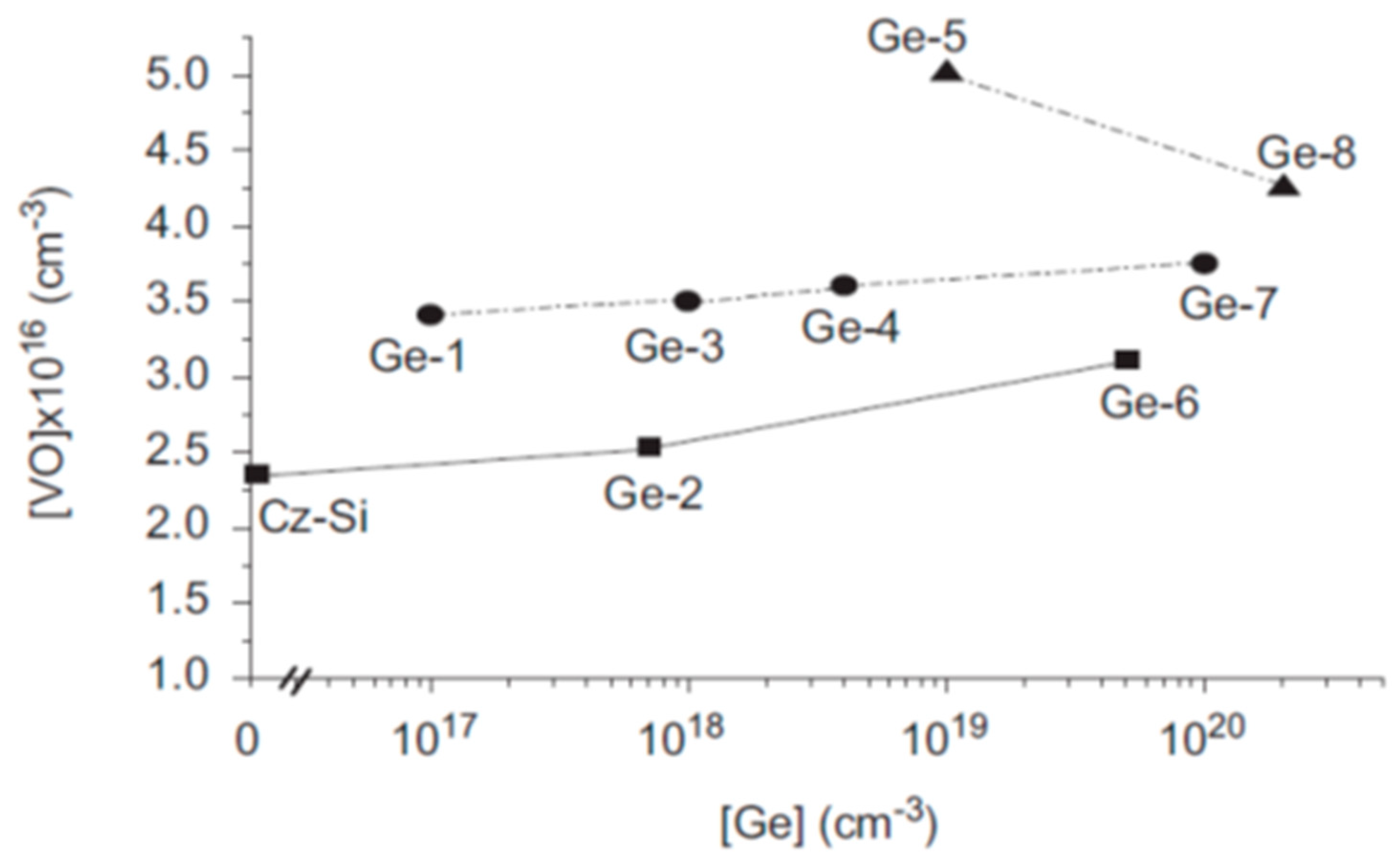
2.3. Production of VO Defects Versus Ge Dopant Concentration
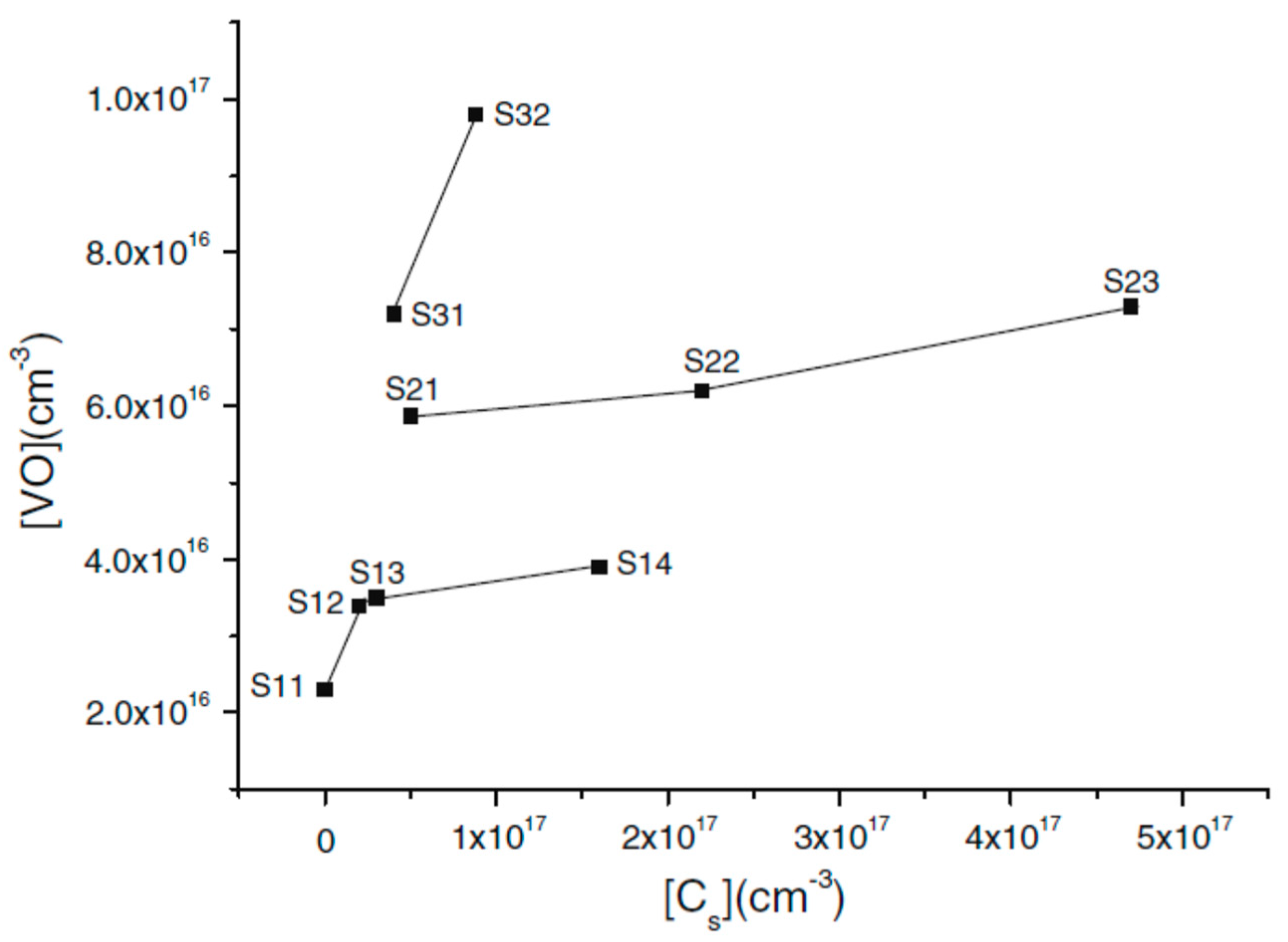
2.4. Conversion of VO to VO2 Defect Versus Ge Dopant Concentration
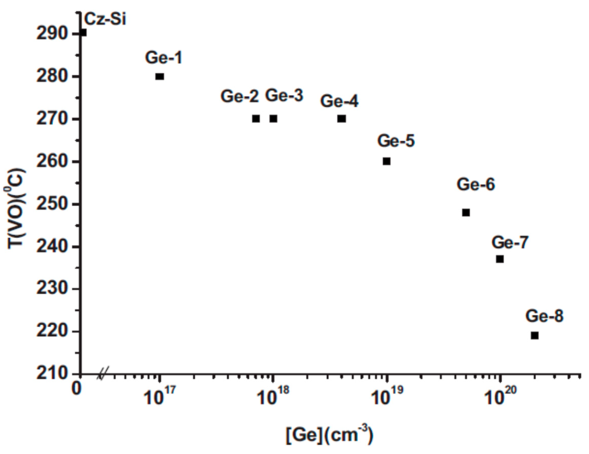
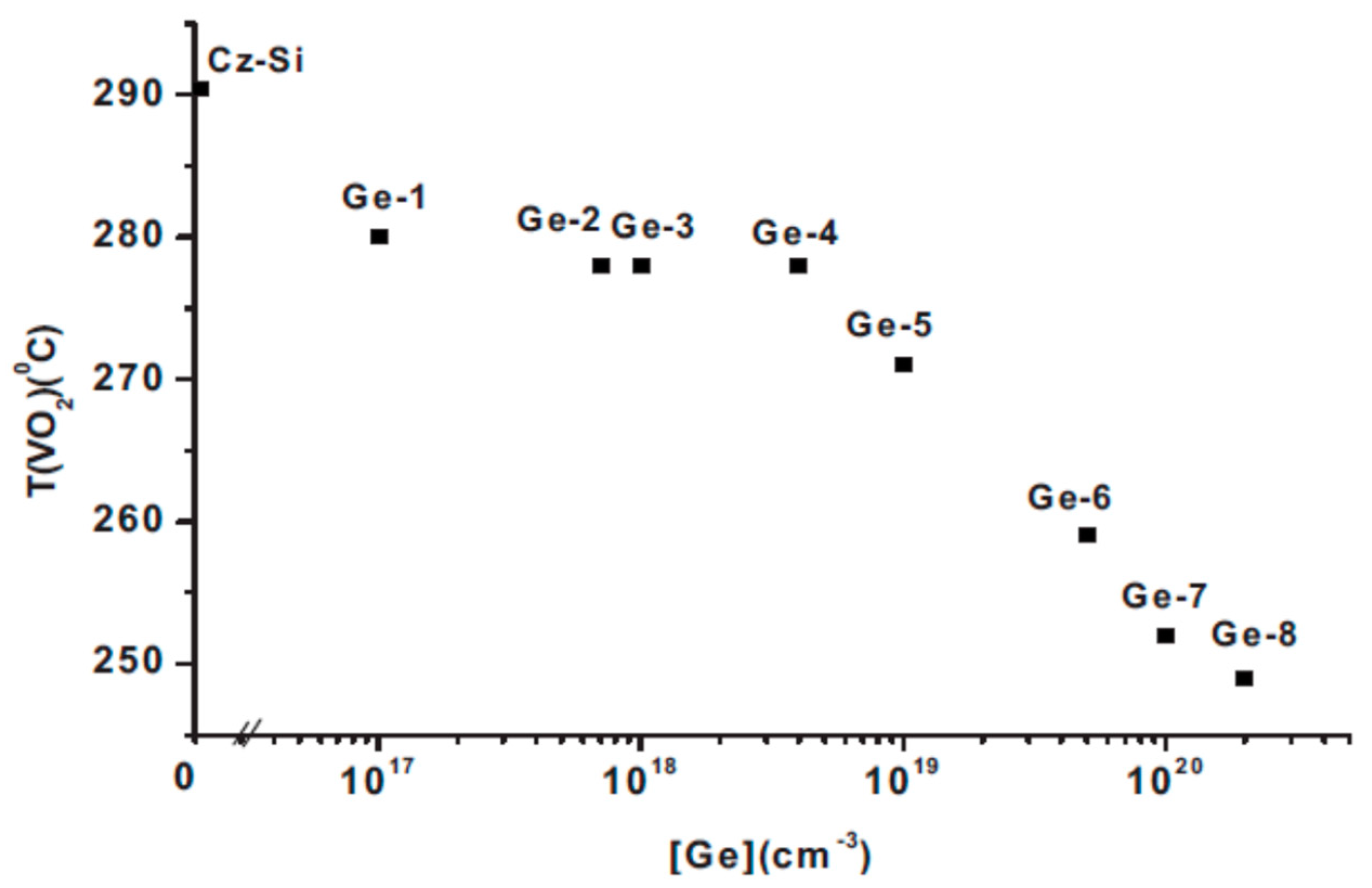
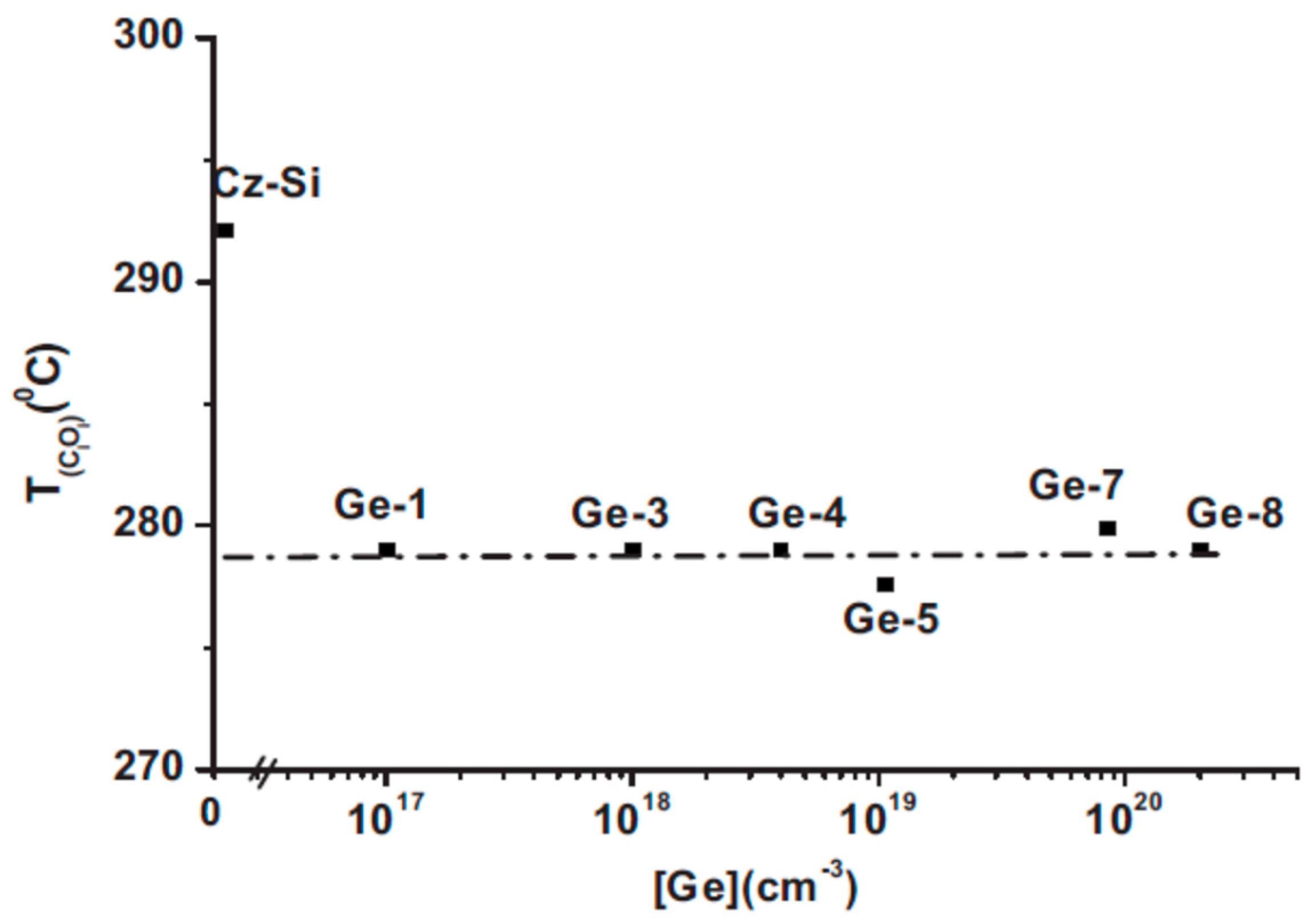
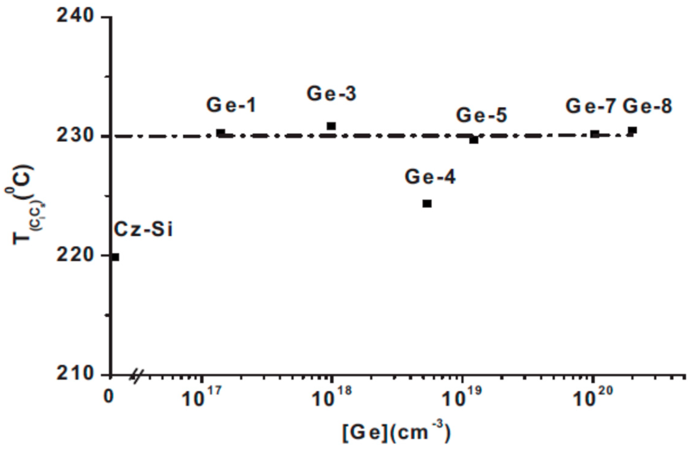
2.5. The Effect of the Ge Dopant Concentration on the Tann of the VO and the Tform of the VO2 Defects
2.6. Production of VO Defect Versus C Concentration
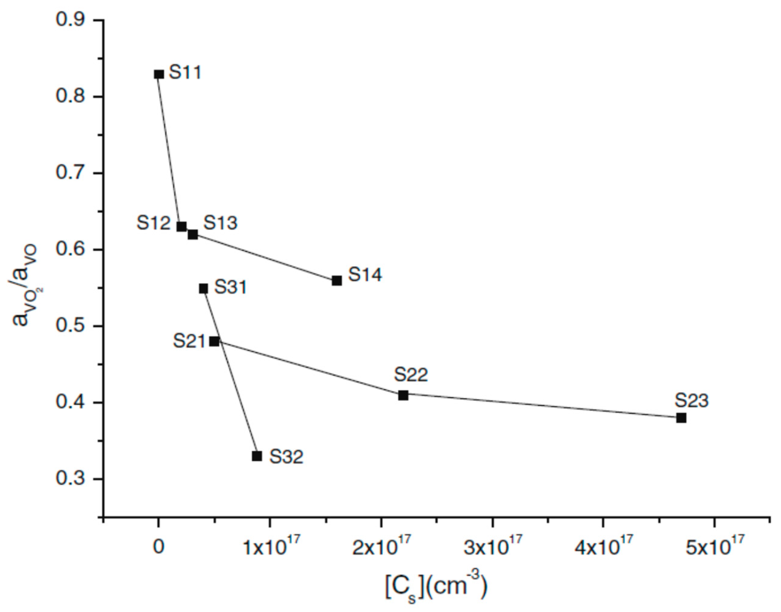
2.7. Conversion of VO to VO2 Defect Versus C Concentration
3. Summary and Future Directions
Funding
Institutional Review Board Statement
Informed Consent Statement
Data Availability Statement
Conflicts of Interest
References
- Shi, L.; Nihtianov, S. Comparative Study of Silicon-Based Ultraviolet Photodetectors. IEEE Sens. J. 2012, 12, 2453–2459. [Google Scholar] [CrossRef]
- Andreani, L.C.; Bozzola, A.; Kowalczewski, P.; Liscidini, M.; Redorici, L. Silicon solar cells: Towards the efficiency limits. Adv. Phys. X 2019, 4, 1548305. [Google Scholar] [CrossRef]
- Atabaki, A.H.; Moazeni, S.; Pavanello, F.; Gevorgyan, H.; Notaros, J.; Alloatti, L.; Wade, M.T.; Sun, C.; Kruger, S.A.; Meng, H.; et al. Integrating photonics with silicon nanoelectronics for the next generation of systems on the chips. Nature 2018, 556, 349–354. [Google Scholar] [CrossRef] [PubMed]
- Petriev, V.M.; Tischenko, V.K.; Mikhailovskaya, A.A.; Popov, A.A.; Tselikov, G.; Zelepukin, I.; Deyev, S.M.; Kaprin, A.D.; Ivanov, S.; Timoshenko, V.Y.; et al. Nuclear nanomedicine using Si nanoparticles as safe and effective carriers of 188Re radionuclide for cancer therapy. Sci. Rep. 2019, 9, 2017. [Google Scholar] [CrossRef] [PubMed]
- Schreiber, L.R.; Bluhm, H. Toward a silicon-based quantum computer. Science 2018, 359, 393–394. [Google Scholar] [CrossRef] [PubMed]
- Reed, G.T. The optical age of silicon. Nature 2004, 427, 595–596. [Google Scholar] [CrossRef]
- Adinolfi, V.; Sargent, E.H. Photovoltage field-effect transistors. Nature 2017, 542, 324–327. [Google Scholar] [CrossRef]
- Jung, Y.H.; Chang, T.-H.; Zhang, H.; Yao, C.; Zheng, Q.; Yang, V.W.; Mi, H.; Kim, M.; Cho, S.J.; Park, D.-W.; et al. High-performance green flexible electronics based on biodegradable cellulose nanofibril paper. Nat. Commun. 2015, 6, 7170. [Google Scholar]
- Corbett, J.W.; Watkins, G.D.; Mc Doland, R.S. New oxygen infrared bands in annealed irradiated silicon. Phys. Rev. 1964, 135, A1381–A1385. [Google Scholar] [CrossRef]
- Londos, C.A. Room-temperature irradiation of p-type silicon. Phys. Stat. Sol. A 1985, 92, 609–614. [Google Scholar] [CrossRef]
- Londos, C.A.; Fytros, L.G.; Georgiou, G.J. IR Studies of Oxygen-vacancy Related Defects in Irradiated Silicon. In Defect and Diffusion Forum; Trans Tech Publications Ltd.: Freienbach, Switzerland, 1999; Volume 171–172, pp. 1–32. [Google Scholar]
- Stein, H.J. Ion-implanted oxygen isotopes in silicon, in Defects in Semiconductors. In Materials Science Forum; von Bardeleben, H.J., Ed.; Trans Tech Publications Ltd.: Freienbach, Switzerland, 1986; Volumes 10–12, pp. 935–940. [Google Scholar]
- Murin, L.I.; Tolkacheva, E.A.; Lastovskii, S.B.; Markevich, V.P.; Mullins, J.; Peaker, A.R.; Svensson, B.G. Interaction of radiation-induced self-interstitials with vacancy-oxygen related defects VnO2 (n from 1 to 3) in silicon. Phys. Stat. Solidi A 2019, 216, 1800609. [Google Scholar] [CrossRef]
- Quemener, V.; Raeissi, B.; Herklotz, F.; Murin, L.I.; Monakhov, E.V.; Svensson, B.G. Kinetic study of the evolution of oxygen-related defects in monocrystalline silicon subjected to electron-irradiation and thermal treatment. J. Appl. Phys. 2015, 118, 135703. [Google Scholar] [CrossRef]
- Markevich, V.P.; Peaker, A.R.; Hamilton, B.; Lastovskii, S.B.; Murin, L.I.; Coutinho, J.; Torres, V.J.B.; Dobaczewski, L.; Svensson, B.G. Structure and electronic properties of trivacancy-oxygen complexes in silicon. Phys. Stat. Solidi A 2011, 208, 568–571. [Google Scholar] [CrossRef]
- Davies, G.; Newman, R.C. Carbon in Monocrystalline Silicon. In Handbook on Semiconductors, Materials Properties and Preparations; Moss, T.S., Mahajan, S., Eds.; Elsevier: Amsterdam, The Netherlands, 1994; Volume 3, pp. 1557–1635. [Google Scholar]
- Londos, C.A. Annealing studies of defects pertinent to radiation damage in Si:B. Phys. Stat. Sol. A 1987, 102, 639–644. [Google Scholar] [CrossRef]
- Ferenzi, G.; Londos, C.A.; Pavelka, T.; Somogyi, M.; Mertens, A. Correlation of the concentration of the carbon-associated radiation damage levels with the total carbon concentration in silicon. J. Appl. Phys. 1988, 63, 183–189. [Google Scholar] [CrossRef]
- Backland, B.J.; Estreicher, S.K. C4 defect and its precursors in Si: First-principles study. Phys. Rev. B 2008, 77, 205205. [Google Scholar] [CrossRef]
- Londos, C.A.; Aliprantis, D.N.; Antonaras, G.; Potsidi, M.S.; Angeletos, T. Angeletos, Experimental and theoretical study of the C4 defect in neutronirradiated silicon. J. Appl. Phys. 2018, 123, 145702. [Google Scholar] [CrossRef]
- Chroneos, A.; Sgourou, E.N.; Londos, C.A.; Schwingenschlogl, U. Oxygen defect processes in silicon and silicon germanium. App. Phys. Rev. 2015, 2, 021306. [Google Scholar] [CrossRef]
- Wang, H.; Chroneos, A.; Sgourou, E.N.; Londos, C.A.; Schwingenschlogl, U. Carbon related defects in irradiated silicon revisited. Sci. Rep. 2014, 4, 4909. [Google Scholar] [CrossRef] [PubMed]
- Zhu, L.; Yuan, S.; Zeng, C.; Xia, J. Manipulating photoluminescence of carbon G-center in silicon metasurface with optical bound states in the continuum. Adv. Opt. Mater. 2020, 8, 1901830. [Google Scholar] [CrossRef]
- Lavrov, E.V.; Nielsen, B.B.; Byberg, J.R.; Hourasine, B.; Jones, R.; Oberg, S.; Briddon, P.R. Local vibrational modes of two neighboring carbon atoms in silicon. Phys. Rev. B 2000, 62, 158–165. [Google Scholar] [CrossRef]
- Timerkaeva, D.; Attaccalite, C.; Brenet, G.; Kaliste, D.; Pochet, P. Structural, electronic and optical properties of the C-C complex in bulk silicon from first principles. J. Appl. Phys. 2018, 123, 161421. [Google Scholar] [CrossRef]
- Brotherton, S.D.; Bradley, P. Defect production and lifetime control in electron and γ-irradiated silicon. Appl. Phys. 1982, 53, 5720–5732. [Google Scholar] [CrossRef]
- Khan, A.; Yamaguchi, M.; Ohshita, Y.; Dharmarasu, N.; Araki, K.; Abe, T.; Itoh, H.; Ohshima, T.; Imaizumi, M.; Matsuda, S. Role of impurities in the production rates of radiation-induced defects in silicon materials and solar cells. J. Appl. Phys. 2001, 90, 1170–1178. [Google Scholar] [CrossRef]
- Hallen, A.; Keskitalo, N.; Masszy, F.; Nagl, V. Lifetime in proton irradiated silicon. J. Appl. Phys. 1996, 79, 3906–3914. [Google Scholar] [CrossRef]
- Beauflis, C.; Redjem, W.; Rousseau, E.; Jacques, V.; Kuznetsov, A.Y.; Raynaud, C.; Voisin, C.; Benali, A.; Herzig, T.; Pezzagna, S.; et al. Optical properties of an ensemble of G-centers in silicon. Phys. Rev. B 2017, 97, 035303. [Google Scholar] [CrossRef]
- Tsuchiya, D.; Sueoka, K.; Yamamoto, H. Density functional theory study of defect behavior related to the bulk lifetime of silicon crystals for power device application. Phys. Stat. Solidi A 2019, 216, 1800615. [Google Scholar] [CrossRef]
- Murata, K.; Yasutake, Y.; Nittoh, K.; Fukatsu, S.; Miki, K. High-density G-centers, light-emitting point defects in silicon crystal. AIP Adv. 2011, 1, 032125. [Google Scholar] [CrossRef]
- Berhanuddin, D.B.; Lourenco, M.A.; Cwilliam, R.M.; Homewood, K.P. Co-implantation of carbon and protons: An integrated silicon device technology compatible method to generate the laser G-center. Adv. Funct. Mater. 2012, 22, 2709–2712. [Google Scholar] [CrossRef]
- Canham, L.T.; Dyball, M.R.; Barraclough, K.G. A study of carbon-implanted silicon for light-emitting diode fabrication. Mater. Sci. Eng. 1989, B4, 95–99. [Google Scholar] [CrossRef]
- Herzig, T.; Rucke, P.; Raaz, N.; Spemann, D.; Redjem, W.; Gerlach, J.W.; Meijer, J.; Cassabois, G.; Abbarchi, M.; Pezzagna, S. Creation of quantum centers in silicon using spatial selective ion implantation of high lateral resolution. In Proceedings of the 22nd International Conference on Ion Implantation Technology, Würzburg, Germany, 16–21 September 2018; pp. 136–139. [Google Scholar]
- Yang, D.; Yu, X.; Ma, X.; Xu, J.; Li, L.; Que, D. Germanium effect on void defects in Czochralski silicon. J. Cryst. Growth 2002, 243, 371–374. [Google Scholar] [CrossRef]
- Watkins, G.D. Intrinsic defects in silicon. Mater. Sci. Semicond. Process. 2000, 3, 227–235. [Google Scholar] [CrossRef]
- Londos, C.A.; Andrianakis, A.; Emtsev, V.V.; Oganesyan, G.A.; Ohyama, H. Effects of germanium doping on the behavior of oxygen and carbon impurities and impurity-related complexes in Si. Phys. B 2009, 404, 4693–4697. [Google Scholar] [CrossRef]
- Vanhellemont, J.; Yasuda, H.; Tokumoto, Y.; Ohno, Y.; Suezawa, M.; Yonenaga, I. 2 MeV e-irradiation UHVEM study on the impact of O and Ge doping on the {113}- defect formation in Si. Phys. Stat. Solidi A 2012, 209, 1902–1907. [Google Scholar] [CrossRef]
- Neimash, V.B.; Kraitchinskii, A.; Kras’ko, M.; Puzenko, O.; Clays, C.; Simoen, E.; Svensson, B.; Kuznetsov, A. Influence of tin impurities on the generation and annealing of thermal oxygen donors in czochralski silicon at 450 °C. J. Electroch. Soc. 2000, 147, 2727–2733. [Google Scholar] [CrossRef]
- Pichler, P. Chapter 4, Isovalent Impurities, (Computational Microelectronics). In Intrinsic Point Defects, Impurities, and Their Diffusion in Siicon; Selberherr, S., Ed.; Spinger/Wien: Vienna, Austria, 2004; pp. 281–329. [Google Scholar]
- Gao, B.; Kakimoto, K. Carbon impurity in crystalline silicon. In Handbook of Photovoltaic Silicon; Yang, D., Ed.; Springer: Berlin/Heidelberg, Germany, 2019; pp. 1–26. [Google Scholar]
- Watkins, G.D. A review of EPR studies in irradiated silicon. In Radiation Damage in Semiconductors; Dunod: Paris, France, 1995; pp. 97–113. [Google Scholar]
- Newman, R.C. Carbon in crystalline silicon, in Oxygen, Carbon, Hydrogen and Nitrogen in Crystalline Silicon. Mater. Res. Soc. Symp. Proc. 1986, 59, 403–417. [Google Scholar] [CrossRef]
- Londos, C.A.; Sgourou, E.N.; Chroneos, A. Oxygen-vacancy defects in electron-irradiated Si: The role of carbon in their behavior. J. Mater. Sci Mater Electron. 2014, 25, 914–921. [Google Scholar] [CrossRef]
- Goesele, U.; Laveant, P.; Scholz, R.; Engler, N.; Werner, P. Diffusion engineering by carbon in Silicon, in Si Front-End Processing- Physics and Technology of Dopant-defect Interaction II. Mater. Res. Soc. Symp. Proc. 2000, 610, B7.1.1–B7.1.12. [Google Scholar]
- Tu, Y.; Shimizu, Y.; Kunimune, Y.; Shimada, Y.; Katayama, T.; Ide, T.; Inoue, M.; Yano, F.; Inoue, K.; Nagai, Y. Effect of carbon diffusion and clustering in silicon: Temperature dependence study. J. Appl. Phys. 2018, 124, 155702. [Google Scholar] [CrossRef]
- Liao, H.-C.; Lin, J.-C.; Chang, R.D. Deactivation of phosphorus by carbon in recrystallized silicon. ECS J. Solid State Sci. Technol. 2019, 8, P262–P266. [Google Scholar] [CrossRef]
- Nakai, K.; Kitahara, K.; Ohta, Y.; Ikari, A.; Tanaka, M. Crystal defects in epitaxial layer on nitrogen-doped czochralski-grown silicon substrate (II)-Suppression of the crystal defects in epitaxial layer by the control of crystal growth condition and carbon co-doping-. Jpn. J. Appl. Phys. 2004, 43, 1247–1253. [Google Scholar] [CrossRef]
- Zhang, J.; Tse, K.; Wong, M.; Zhang, Y.; Zhu, J. A brief review of co-doping. Front. Phys. 2016, 11, 117405. [Google Scholar] [CrossRef]
- Yang, D.; Chen, J.; Ma, X.; Que, D. Impurity engineering of Czochralski silicon used for ultra large-scaled-integrated circuits. J. Cryst. Growth 2009, 311, 837–841. [Google Scholar] [CrossRef]
- Voronkov, V.V.; Falster, R.; Londos, C.A.; Sgourou, E.N.; Andrianakis, A.; Ohyama, H. Production of vacancy-oxygen defect in electron irradiated silicon in the presence of self-interstitial-trapping impurities. J. Appl. Phys. 2011, 110, 093510. [Google Scholar] [CrossRef]
- Brelot, A. Tin as a vacancy trap in silicon at room temperature. IEEE Trans. Nucl. Sci. 1972, 19, 220–223. [Google Scholar] [CrossRef]
- Lavrov, E.V.; Fanciulli, M.; Kaukonen, M.; Jones, R.; Briddon, P.R. Carbon-tin defects in silicon. Phys. Rev. B 2001, 64, 125212. [Google Scholar] [CrossRef]
- David, M.L.; Simoen, E.; Clays, C.; Neimash, V.B.; Kra’sko, M.; Kraitchinskii, A.; Voytovych, V.; Kabaldin, A.; Barbot, J.F. Electrically active defects in irradiated n-type czochralski silicon doped with group IV impurities. J. Phys. Condens. Matter 2005, 17, S2255–S2266. [Google Scholar] [CrossRef]
- Milants, K.; Verheyden, J.; Balancira, T.; Deweerd, W.; Pattyn, H.; Bukshpan, S.; Williamson, D.L.; Vermeiren, F.; Van Tendeloo, G.; Viekken, C.; et al. Size distribution and magnetic behavior of lead inclusions in silicon single crystals. J. Appl. Phys. 1997, 81, 2148–2152. [Google Scholar] [CrossRef]
- Chen, J.; Yang, D.; Ma, X.; Zeng, Z.; Tian, D.; Li, L.; Que, D.; Gong, L. Influence of germanium doping on the mechanical strength of Czochralski silicon wafers. J. Appl. Phys. 2008, 103, 123521. [Google Scholar] [CrossRef]
- Chen, J.; Yang, D.; Ma, X.; Que, D. Rapid-thermal-anneal-based internet gettering for germanium-doped Czochralski silicon. Appl. Phys. A 2009, 94, 905–910. [Google Scholar] [CrossRef]
- Yang, D. Defects in germanium-doped Czochralski silicon. Phys. Stat. Sol. A 2005, 202, 931–938. [Google Scholar] [CrossRef]
- Vanhellemont, V.; Chen, J.; Xu, W.; Yang, D.; Rafi, J.M.; Ohyama, H.; Simoen, E. Germanium doping of Si substrates for improved device characteristics and Yield. ECS Trans. 2010, 27, 1041–1046. [Google Scholar] [CrossRef]
- Chen, J.; Yang, D.; Li, H.; Ma, X.; Tian, D.; Li, L.; Que, D. Crystal-originated particles in germanium-doped Czochralski silicon crystal. J. Cryst. Growth. 2007, 306, 262–268. [Google Scholar] [CrossRef]
- Tanay, F.; Dubois, S.; Enjalbert, N.; Veirman, J.; Gidon, P.; Perichaud, I. Effects of germanium doping on the boron-oxygen complex formation in silicon solar cells. Phys. Stat. Solidi C 2012, 9, 1981–1986. [Google Scholar] [CrossRef]
- Yu, X.; Yang, P.; Chen, P.; Li, X.; Yang, D. Suppression of boron oxygen defects in p-type Czochralski silicon by germanium doping. Appl. Phys. Lett. 2010, 97, 051903. [Google Scholar] [CrossRef]
- Yonenaga, I.; Taishi, T.; Huang, X.; Hoshikawa, K. Dynamic characteristics of dislocations in ge-doped and (Ge + B) codoped silicon. J. Appl. Phys. 2003, 93, 265–269. [Google Scholar] [CrossRef]
- Arivandhan, M.; Gotoh, R.; Fujiwara, K.; Uda, S. Effects of B and Ge codoping on the minority carrier lifetime in Ga-doped Czochralski silicon. J. Appl. Phys. 2009, 106, 013721. [Google Scholar] [CrossRef]
- Vanhellemont, V.; Anada, S.; Nagase, T.; Yasuda, H.; Schulze, A.; Bender, H.; Rooyackers, R.; Vandooren, A. Impact of dopants and silicon structure dimensions on {113}-defect formation during 2MeV electron irradiation in an UHVEM. Phys. Status Solidi C 2015, 12, 1160–1165. [Google Scholar] [CrossRef]
- Ahn, C.; Bennett, N.; Dunham, S.T.; Cowern, N.E. Stress effects on impurity solubility in crystalline materials: A general model and density-functional calculations for dopants in silicon. Phys. Rev. B 2009, 79, 073201. [Google Scholar] [CrossRef]
- Ikuta, T.; Miyanami, Y.; Fujita, S.; Iwamoto, H.; Kadomura, S.; Shimura, T.; Watanabe, H.; Yasutake, K. Atmospheric in situ arsenic-doped SiGe selective epitaxial growth for Raised-extension n-type metal-oxide-semiconductor field–effect transistor. Jpn J. Appl. Phys. 2007, 40, 1916–1920. [Google Scholar] [CrossRef]
- Alesandrov, O.V.; Afonin, N.N. Effect of germanium on redistribution of boron and phosphorus during thermal oxidation of silicon. Semicond. Sci. Technol. 2003, 18, 139–143. [Google Scholar] [CrossRef]
- Brelot, A.; Charlemagne, J. Infrared studies of low temperature electron irradiated silicon containing germanium oxygen and carbon. Radiat. Eff. 1971, 9, 65–73. [Google Scholar] [CrossRef]
- Chen, J.; Wu, T.; Ma, X.; Wang, L.; Yang, D. Ge-vacancy pair in Ge-doped Czochralski silicon. J. Appl. Phys. 2008, 103, 123519. [Google Scholar] [CrossRef]
- Chroneos, A.; Grimes, P.W.; Bracht, H. Impact of germanium on vacancy clustering in germanium-doped silicon. J. Appl. Phys. 2009, 105, 016102. [Google Scholar] [CrossRef]
- Yeh, T.H.; Joshi, M.L. Strain compensation in silicon by diffused impurities. J. Electrochem. Soc. 1969, 116, 73–77. [Google Scholar] [CrossRef]
- Yagi, K.; Miyamoto, N.; Nishizawa, J.-I. Anomalous diffusion of phosphorus into silicon. Jpn. J. Appl. Phys. 1970, 9, 246–254. [Google Scholar] [CrossRef]
- Claeys, C.; Simoen, E.; Neimash, V.B.; Kraitchinskii, A.; Kras’ko, M.; Puzenko, O.; Blondeel, A.; Clauws, P. Tin doping of silicon for controlling oxygen precipitation and radiation hardness. J. Electrochem. Soc. 2001, 148, G738–G745. [Google Scholar] [CrossRef]
- Matyash, I.; Minailova, I.; Serdega, B. Research of mechanical stresses in irradiated tin-doped silicon crystals. Mater. Sci. Semicond. Process. 2017, 71, 263–267. [Google Scholar] [CrossRef]
- Voronkov, V.V. The mechanism of swirl defects formation in silicon. J. Cryst. Growth 1982, 59, 625–643. [Google Scholar] [CrossRef]
- Sun, J.; He, Q.; Ban, B.; Bai, X.; Li, J.; Chen, J. Effect of Sn doping on improvement of minority carrier lifetime of Fe contaminated p-type multi-crystalline Si ingot. J. Cryst. Growth 2017, 458, 66–71. [Google Scholar] [CrossRef]
- Kras’ko, M.M. Influence of tin impurity on recombination characteristics in γ—irradiated n-Si. Ukr. J. Phys. 2012, 57, 1162–1168. [Google Scholar]
- Kras’ko, M.M. Influence of tin impurity on degradation of conductivity in electron-irradiated n-Si. Ukr. J. Phys. 2013, 58, 243–248. [Google Scholar] [CrossRef]
- Wijaranakula, W. A quantitative model for an interaction between extended dislocations loops and impurities in Czochralski silicon based upon the photoluminescence analysis. J. Appl. Phys. 1991, 70, 3018–3024. [Google Scholar] [CrossRef]
- Gao, C.; Ma, X.; Yang, D. Density functional theory study of the impact of tin doping on oxygen diffusion in Czochralski silicon. Phys. Status Solidi A 2013, 210, 2199–2203. [Google Scholar] [CrossRef]
- Gao, C.; Ma, X.; Zhao, J.; Yang, D. Effect of tin on point defects and oxygen precipitation in Czochralski silicon: Experimental and theoretical studies. J. Appl. Phys. 2013, 113, 093511. [Google Scholar] [CrossRef]
- Wijaranakula, W. Oxygen precipitation and thermal donor formation in Czochralski-grown silicon doped with carbon and tin. J. Appl. Phys. 1991, 69, 2737–2739. [Google Scholar] [CrossRef]
- Scheffler, L.; Roesgaard, R.; Harsen, J.L.; Larsen, A.N.; Julsgaard, B. Tin-based donors in SiSn alloys. J. Appl. Phys. 2019, 126, 035702. [Google Scholar] [CrossRef]
- Yonenaga, I.; Taishi, T.; Inoue, K.; Gotoh, R.; Kutsukake, K.; Tokumoto, Y.; Ohno, Y. Czochralski growth of heavily tin-doped Si crystals. J. Cryst. Growth 2014, 395, 94–97. [Google Scholar] [CrossRef]
- Jiang, X.; Li, M.; Ming, Y.; Wang, J.; Li, W. The structure and properties of Sn/SiSn-nanodisperse alloy thin films. IOP Conf. Ser. Mater. Sci. Eng. 2019, 654, 012010. [Google Scholar] [CrossRef]
- Watkins, G.D.; Troxell, J.R. Negative-U properties for point defects in silicon. Phys. Rev. Lett. 1980, 4, 593–596. [Google Scholar] [CrossRef]
- Watkins, G.D. Defects in irradiated silicon: EPR of tin-vacancy pair. Phys. Rev. B 1975, 19, 4383–4390. [Google Scholar] [CrossRef]
- Svensson, B.G.; Svensson, J.; Lindrstrom, J.L.; Davies, G.; Corbett, J.W. Generation of divacancies in tin-doped silicon. Appl. Phys. Lett. 1987, 51, 2257–2259. [Google Scholar] [CrossRef]
- Svensson, B.G.; Lindrstrom, J.L. Generation of divscancies in silicon by MeV electrons: Dose rate dependence and influence of Sn and P. J. Appl. Phys. 1992, 72, 5616–5621. [Google Scholar] [CrossRef]
- Fanciulli, M.; Byberg, J.R. Divacancy-tin complexes in electron-irradiated silicon studied by EPR. Phys. Rev.B 2000, 61, 2657–2671. [Google Scholar] [CrossRef]
- Larsen, A.N.; Goobet, J.J.; Mejlholm, M.; Christensen, J.S.; Fanciullil, M.; Gunnluogsson, H.P.; Weyer, G.; Petersen, J.W.; Resende, A.; Kaukonen, M.; et al. Tin-vacancy acceptor levels in electron-irradiated n-type silicon. Phys. Rev. B 2000, 62, 4535–4544. [Google Scholar] [CrossRef]
- Chroneos, A.; Londos, C.A.; Sgourou, E.N.; Pochet, P. Point defect engineering strategies to suppress A-center formation in silicon. Appl. Phys. Lett. 2011, 99, 241901. [Google Scholar] [CrossRef]
- Fanciulli, M.; Byberg, J.R. Tin-vacancy complexes in electron-irradiated n-type silicon. Phys. B 1999, 273–274, 524–527. [Google Scholar] [CrossRef]
- Ruzin, A.; Casse, G.; Glaser, M.; Lemeilleur, F.; Talamonti, R.; Watts, S.; Zanet, A. Radiation hardness of silicon Detectors manufactured on epitaxial material and FZ bulk enriched with oxygen, carbon, tin and platinum, Rose collaboratin-RD48. Nucl. Phys. B 1999, 78, 645–649. [Google Scholar] [CrossRef]
- Lindstrom, G.; Moll, M.; Fretwurst, E. Radiation hardness of silicon detectors—A challenge from high-energy physics. Nucl. Instrum. Meth. Phys. Res. A 1999, 426, 1–15. [Google Scholar] [CrossRef]
- Kanneboina, V.; Basumatary, P.; Agarwal, P. Influence of deposition temperature on indium tin oxide thin films for solar cell applications. AIP Conf. Proc. 2019, 2091, 020016. [Google Scholar]
- Werner, J.; Oehme, M.; Schmid, M.; Kaschel, M.; Schirmer, A.; Kasper, E.; Schulze, J. Germanium-tin p-i-n photodetectors integrated on silicon grown by molecular beam epitaxy. App. Phys. Lett. 2011, 98, 061108. [Google Scholar] [CrossRef]
- Simoen, E.; Clays, C.; Neimash, V.B.; Kraitchinskii, A.; Kra’sko, N.; Puzenko, O.; Blondeel, A.; Clauws, P. Deep levels in high-energy proton-irradiated tin-doped n-type Czochralski silicon. Appl. Phys. Lett. 2000, 76, 2838–2840. [Google Scholar] [CrossRef]
- Chroneos, A.; Londos, C.A.; Sgourou, E.N. Effect of tin doping on oxygen-and carbon-related defects in Czochralski silicon. J. Appl. Phys. 2011, 110, 093507. [Google Scholar] [CrossRef]
- David, M.-L.; Simoen, E.; Clays, C.; Neimash, V.B.; Kra’sko, M.; Kraitchinskii, A.; Voytovych, V.; Tishchenko, V.; Barbot, J.F. Radiation-induced deep l;evels in lead and tin doped n-type Czochralski silicon. In Proceedings of the High Purity Silicon VIII, Honolulu, HI, USA, 3–8 October 2004; pp. 395–406. [Google Scholar]
- Londos, C.A.; Aliprantis, D.; Sgourou, E.N.; Chroneos, A.; Pochet, P. Formation and evolution of oxygen-vacancy clusters in lead and tin doped silicon. J. Appl. Phys. 2012, 111, 123508. [Google Scholar] [CrossRef]
- Canham, I.T.; Barraclough, K.G.; Robbins, D.J. 1.3 μm light-emitting diode from silicon electron-irradiated at damage threshold. Appl. Phys. Lett. 1987, 51, 1509–1511. [Google Scholar] [CrossRef]
- Neimash, V.B.; Voytovych, V.; Kra’sko, M.; Kraitchinskii, A.; Kabaldin, O.M.; Pavlovs’kyi, Y.V.; Tsmots, V.M. Formation of radiation-induced defects in n-Si with lead and carbon impurities. Ukr. J. Phys. 2005, 50, 1273–1277. [Google Scholar]
- Neimash, V.B.; Voytovych, V.; Kraitchinskii, A.M.; Shpinar, L.I.; Kra’sko, M.M.; Popov, V.M.; Pokanevygh, A.P.; Gorodys’kyi, M.I.; Pavlovs’kyi, Y.V.; Tsmots, V.M.; et al. Influence of doping by the isovalent lead impurity on the parameters of n-silicon. Ukr. J. Phys. 2005, 50, 492–496. [Google Scholar]
- Kras’ko, M.M.; Voytovych, V.V.; Neimash, V.B.; Kraitchinskii, A. Effect of doping by lead on the formation of thermal defects in silicon with increased carbon concentration. Ukr. J. Phys. 2004, 49, 691–694. [Google Scholar]
- Neimash, V.B.; Kra’sko, M.; Kraitchinskii, A.; Voytovych, V.; Kabaldin, O.; Tsmots, V.; Simoen, E.; Clays, C. Oxygen precipitation and thermal donor formation in Pb and C-doped n-type Czochralski silicon. In Proceedings of the High Purity Silicon VIII, Honolulu, HI, USA, 3–8 October 2004; pp. 286–293. [Google Scholar]
- Sgourou, E.N.; Timerkaeva, D.; Londos, C.A.; Aliprantis, D.; Chroneos, A.; Caliste, D.; Pochet, P. Impact of isovalent doping on the trapping of vacancy and interstitial related defects in Si. J. Appl. Phys. 2013, 113, 113506. [Google Scholar] [CrossRef]
- David, M.L.; Simoen, E.; Clays, C.; Neimash, V.B.; Kra’sko, M.; Kraitchinskii, A.; Voytovych, V.; Kabaldin, A.; Barbot, J.F. On the effect of lead on irradiation induced defects in silicon. Solid State Phenom. 2005, 108–109, 373–378. [Google Scholar] [CrossRef]
- Ji, P.-f.; Wang, C.; Yang, J.; Shi, Z.-S.; Yang, Y. Photoelectric properties of the doped silicon with carbon family elements. Adv. Mat. Res. 2014, 873, 793–798. [Google Scholar] [CrossRef]
- Vanhellemont, J.; Suezawa, M.; Yonenaga, I. On the impact of germanium doping on the vacancy formation energy in czochralski-grown silicon. J. Appl. Phys. 2010, 108, 016105. [Google Scholar] [CrossRef]
- Sueoka, K.; Kamiyama, E.; Vanhellemont, J. Density functional theory study on the impact of heavily doping on Si intrinsic point defect properties and implications for single crystal growth from the melt. J. Appl. Phys. 2013, 114, 153510. [Google Scholar] [CrossRef]
- Matyash, I.E.; Minailova, I.A.; Serdega, B.K.; Khirunenko, L.I. Residual stresses in Si and their evolution upon heat treatment and irradiation. Semiconductors 2017, 51, 1107–1110. [Google Scholar] [CrossRef]
- Segall, M.D.; Lindan, P.J.D.; Probert, M.J.; Pickard, C.J.; Hasnip, P.J.; Clark, S.J.; Payne, M.C. First-principles simulation: Ideas, illustrations and CASTEP code. J. Phys. Condens. Matter 2002, 14, 2717–2744. [Google Scholar] [CrossRef]
- Rupasov, D.; Chroneos, A.; Parfitt, D.; Kilner, J.A.; Grimes, R.W.; Istomin, S.Y.; Antipov, E.V. Oxygen diffusion in Sr0.75Y0.25CoO2.625: A molecular dynamics study. Phys. Rev. B 2009, 79, 172102. [Google Scholar] [CrossRef]
- Chroneos, A.; Jiang, C.; Grimes, R.W.; Schwingenschlögl, U.; Bracht, H. E-centers in ternary Si1-x-yGexSny random alloys. Appl. Phys. Lett. 2009, 95, 112101. [Google Scholar] [CrossRef]
- Murphy, S.T.; Chroneos, A.; Jiang, C.; Schwingenschlögl, U.; Grimes, R.W. Deviations from Vegard’s law in ternary III-V alloys. Phys. Rev. B 2010, 82, 073201. [Google Scholar] [CrossRef]
- Kushima, A.; Yildiz, B. Oxygen ion diffusivity in strained yttria stabilized zirconia: Where is the fastest strain? J. Mater. Chem. 2010, 20, 4809–4819. [Google Scholar] [CrossRef]
- Chroneos, A.; Grimes, R.W.; Bracht, H. Fluorine codoping in germanium to suppress donor diffusion and deactivation. J. Appl. Phys. 2009, 106, 063707. [Google Scholar] [CrossRef]
- Chroneos, A. Isovalent impurity-vacancy complexes in germanium. Phys. Stat. Sol. B 2007, 244, 3206–3210. [Google Scholar] [CrossRef]
- Bracht, H.; Chroneos, A. The vacancy in silicon: A critical evaluation of experimental and theoretical results. J. Appl. Phys. 2008, 104, 076108. [Google Scholar] [CrossRef]
- Wang, H.; Chroneos, A.; Londos, C.A.; Sgourou, E.N.; Schwingenschlögl, U. A-centers in silicon studied with hybrid density functional theory. Appl. Phys. Lett. 2013, 103, 052101. [Google Scholar] [CrossRef]
- Wang, H.; Chroneos, A.; Londos, C.A.; Sgourou, E.N.; Schwingenschlögl, U. Doping strategies to control A-centers in silicon: Insights from hybrid density functional theory. Phys Chem. Chem. Phys. 2014, 16, 8487–8492. [Google Scholar] [CrossRef]
- Borchi, E.; Bruzzi, M. Radiation damage in silicon detectors. Rivista Nuovo Cimento 1994, 17, 1–63. [Google Scholar] [CrossRef]
- Clays, C.; Simoen, E.; Eneman, G.; Ni, K.; Hikavyy, A.; Loo, R.; Gupta, S.; Merckling, C.; Alian, A.; Caymax, M. Review-Device assessment of electrically active defects in high-mobility materials. JCS J. Sol. State Sci. Technol. 2016, 5, P3149–P3165. [Google Scholar] [CrossRef]
- Misiuk, A.; Bac-Misiuk, J.; Barcz, A.; Romano-Rodriguez, A.; Antonova, I.V.; Popov, V.P.; Londos, C.A.; Jun, J. Effect of annealing at argon pressure up to 1.2 GPa on hydrogen-plasma-etched and hydrogen-implanted single-crystalline silicon. Int. J. Hydrog. Energy 2011, 26, 483–488. [Google Scholar] [CrossRef]
- Londos, C.A.; Andrianakis, A.; Sgourou, E.N.; Emtsev, V.V.; Ohyama, H. IR studies of the impact of Ge doping on the successive formation of, VOn defects in czochralski-Si containing carbon. J. Appl. Phys. 2011, 109, 033508. [Google Scholar] [CrossRef]
- Londos, C.A.; Andrianakis, A.; Sgourou, E.N.; Emtsev, V.V.; Ohyama, H. Effect of germanium doping on the characteristics of oxygen and carbon-related defects in Czochralski silicon. J. Appl. Phys. 2010, 107, 093520. [Google Scholar] [CrossRef]
- Londos, C.A.; Sarlis, N.V.; Fytros, L.G.; Papastergiou, K. Precursor defect to the vacancy-dioxygen center in, Si. Phys. Rev. B 1996, 53, 6900–6903. [Google Scholar] [CrossRef]
- Murin, L.I.; Lindstrom, J.L.; Svensson, B.G.; Markevich, V.P.; Peaker, A.R.; Londos, C.A. VOn (n≥3) defects in irradiated and heat-treated silicon. Solid State Phenom. 2005, 108–109, 267–272. [Google Scholar] [CrossRef]
- Stein, H.J. Ion-implanted oxygen isotopes in silicon. Mater. Sci. Forum 1986, 10–12, 935–940. [Google Scholar] [CrossRef]
- Svensson, B.G.; Lindstrom, J.L. Annealing studies of the 862 cm-1 infrared band in silicon. Phys. Stat. Sol. A 1986, 95, 537–542. [Google Scholar] [CrossRef]
- Chappell, S.P.; Claybourn, M.; Newman, R.C.; Barraclouth, K.G. The production of CiOi complexes during irradiation of Czochralski silicon at 130 °C. Semicond. Sci. Technol. 1988, 3, 1047–1051. [Google Scholar] [CrossRef]
- Davies, G. Carbon-related processes in crystalline silicon. Mater. Sci. Forum 1989, 38–41, 151–158. [Google Scholar] [CrossRef]
- Lavrov, E.V.; Hoffman, I.; Bech Nielsen, B. Local vibrational modes of the metastable dicarbon center (CsCi) in silicon. Phys. Rev. B 1999, 60, 8081–8086. [Google Scholar] [CrossRef]
- Leary, P.; Jones, R.; Oberg, S.; Torres, V.J.B. Dynamic properties of the interstitial carbon and carbon-carbon defects in silicon. Phys. Rev. B 1997, 55, 2188–2194. [Google Scholar] [CrossRef]
- Angeletos, T.; Chroneos, A.; Londos, C.A. Infrared studies of the evolution of the CiOi(SiI) defect in irradiated Si upon thermal anneals. J. Appl. Phys. 2016, 119, 125704. [Google Scholar] [CrossRef]
- Londos, C.A. Aspects of the defect reactions related to carbon impurity in silicon. Jpn J. Appl. Phys. Part I 1988, 27, 2089–2093. [Google Scholar] [CrossRef]
- Londos, C.A. Carbon-related radiation damage centers and processes in p-type Si. Sci. Technol. 1990, 5, 645–648. [Google Scholar]
- Londos, C.A. Deep-level transient spectroscopy studies of the interstitial carbon defect in silicon. Phys. Rev. B 1987, 35, 6295–6297. [Google Scholar] [CrossRef]
- Londos, C.A.; Andrianakis, A.; Emtsev, V.V.; Ohyama, H. Radiation-induced defects in czochralki silicon containing carbon and germanium. Semicond. Sci. Technol. 2009, 24, 075002. [Google Scholar] [CrossRef]
- Khirunenko, L.I.; Kobzar, O.O.; Pomozov, Y.V.; Sosnin, M.G.; Tripachko, M.O. Peculiarities of vacancy-related defect formation in Si doped wit tin. Phys. B 2003, 340–342, 541–545. [Google Scholar] [CrossRef]
- Londos, C.A.; Sgourou, E.N.; Chroneos, A. Defect engineering of the oxygen-vacancy clusters formation in electro irradiated silicon by iosovalent doping: An infrared perspective. J. Appl. Phys. 2012, 112, 123517. [Google Scholar] [CrossRef]
- Newman, R.C.; Jones, R. Diffusion of oxygen in silicon, in Oxygen in Silicon. In Semiconductors and Semimetals; Shimura, F., Ed.; Elsevier: Orlando, FL, USA, 1994; Volume 42, pp. 289–352. [Google Scholar]
- Sobolev, N.A.; Nazare, M.H. Defects incorporating Ge atoms in irradiated Si:Ge. Phys. B 1999, 273–274, 271–274. [Google Scholar] [CrossRef]
- Cheng, L.J.; Corelli, J.C.; Corbett, J.W.; Watkins, G.D. 1.8-, 3.3-, and 3.9-μ bands in irradiated silicon: Correlations with the divacancy. Phys. Rev. 1966, 152, 761–774. [Google Scholar] [CrossRef]
- Evwaraye, A.O.; Sun, E. Electron-irradiation-induced divacancy in lightly doped silicon. J. Appl. Phys. 1976, 47, 3776–3780. [Google Scholar] [CrossRef]
- Chroneos, A.; Londos, C.A. Interaction of A-centers with isovalent impurities in silicon. J. Appl. Phys. 2010, 107, 093518. [Google Scholar] [CrossRef]
- Lindstrom, J.L.; Svensson, B.G. Oxygen-related defects in silicon. In Oxygen, Carbon, Hydrogen, and Nitrogen in Crystalline Silicon, MRS Symposia Proceedings; Mikkelsen, J.C., Jr., Pearton, S.J., Corbett, J.W., Pennycook, P.W., Eds.; Materials Research Society: Pittsburgh, PN, USA, 1986; Volume 59, pp. 45–58. [Google Scholar]
- Murin, L.I.; Svensson, B.G.; Lindstrom, J.L.; Markevich, V.P.; Londos, C.A. Divacancy-oxygen and Trivacancy-oxygen complexes in silicon: Local vibrational modes studies. Solid State Phenom. 2010, 156–158, 129–134. [Google Scholar] [CrossRef]
- Dong, P.; Yang, P.; Yu, X.; Chen, L.; Ma, Y.; Li, M.; Dai, G.; Zhang, J. Effect of Germanium doping on the production and evolution of divacancy complexes in neutron irradiated czochralski silicon. J. Electron. Mater. 2018, 47, 5019–5024. [Google Scholar] [CrossRef]
- Murin, L.I.; Svensson, B.G.; Lindstrom, J.L.; Markevich, V.P.; Londosm, C.A. Londos, Trivacancy-oxygen complex in silicon: Local vibrational mode characterization. Phys. B 2009, 404, 4568–4571. [Google Scholar] [CrossRef]
- Colbersen, B.O.; Muhlbauer, A. Carbon in silicon: Properties and impact on devices. Solid State Electron. 1982, 25, 759–775. [Google Scholar]
- Gentile, F.S.; Platonenko, A.; El-Kerlani, K.E.; Rerat, M.; D’Arco, P.; Dovesi, R. Substitutional carbon defects in silicon: A quantum mechanical characterization through the infrared and Raman spectra. J. Comput. Chem. 2020, 41, 1638–1644. [Google Scholar] [CrossRef] [PubMed]
- Londos, C.A.; Sgourou, E.N.; Timerkaeva, D.; Chroneos, A.; Pochet, P.; Emtsev, V.V. Impact of isovalent doping on radiation defects in silicon. J. Appl. Phys. 2013, 114, 113504. [Google Scholar] [CrossRef]
- Khirunenko, L.I.; Kobzar, O.O.; Pomozov, Y.V.; Sosnin, M.G.; Tripachko, M.O.; Abrosimov, N.V.; Riemann, H. Interstitial-related reactions in silicon doped with isovalent impurities. Phys. B 2003, 340–342, 546–550. [Google Scholar] [CrossRef]
- Inoue, N.; Ohyama, H.; Goto, Y.; Suriyama, T. Quantitative analysis of complexes in electro irradiated CZ silicon. Phys. B 2007, 401–402, 477–482. [Google Scholar] [CrossRef]
- Londos, C.A.; Sgourou, E.N.; Chroneos, A. Impact of isovalent defect engineering strategies on carbon-related clusters in silicon. J. Mater. Sci. Mater. Electron. 2013, 24, 1696–1701. [Google Scholar] [CrossRef]
- Davies, G.; Kwok, K.T.; Team, R. Annealing kinetics of the dicarbon radiation-damage center in crystalline silicon. Phys. Rev. B 1991, 44, 12146–12157. [Google Scholar] [CrossRef]
- Kwok, K.T. Carbon- and 0xygen-related point defects created by annealing the dicarbon radiation-damage center in crystalline silicon. Phys. Rev. B 1995, 51, 17188–17191. [Google Scholar] [CrossRef] [PubMed]
- Trombetta, J.M.; Watkins, G.D. Identification of an interstitial carbon-related complex in silicon. Appl. Phys. Lett. 1987, 51, 1103–1105. [Google Scholar] [CrossRef]


| Sample Name | [Ge] × 1020 (cm−3) | [Pb] × 1017 (cm−3) | [Sn] × 1017 (cm−3) | [Oi]o × 1017 (cm−3) | [Cs]o × 1016 (cm−3) | Fluence (cm−2) |
|---|---|---|---|---|---|---|
| Cz-Si0 | … | … | … | 9.56 | <2.0 | 5 × 10¹⁷ |
| Cz-Si1 | … | … | … | 10.00 | 16.0 | 5 × 10¹⁷ |
| Ge-8 | 2 | … | … | 7.70 | 18.0 | 5 × 10¹⁷ |
| Cz-Si:Pb | …. | 10 | … | 2.1 | 1.9 | 1 × 10¹⁸ |
| Cz-Si: SnH | … | … | 90 | 9.2 | 2.0 | 1 × 10¹⁸ |
| Cz-Si:SnPb | … | 10 | 2 | 6.2 | 4.0 | 1 × 10¹⁸ |
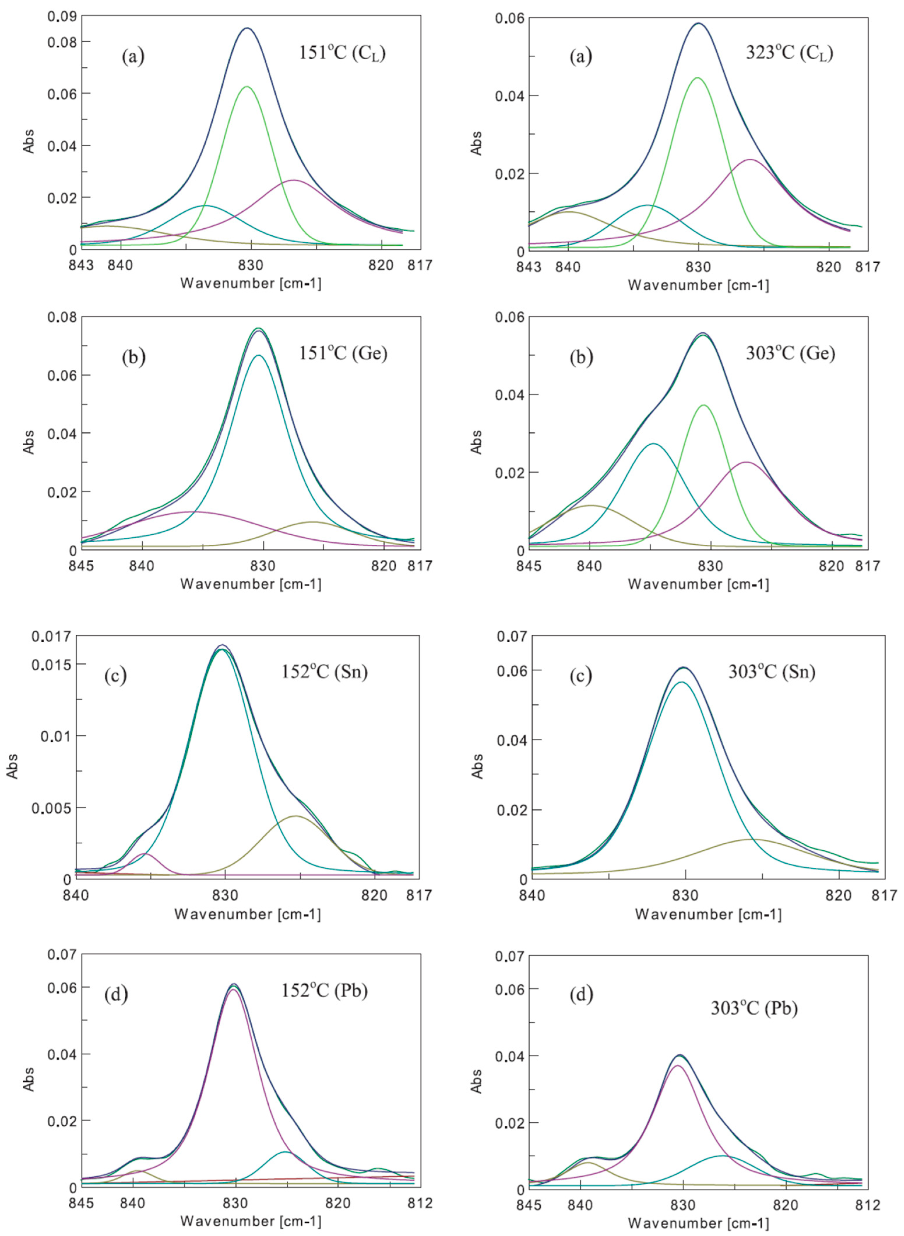
| Sample | Dopant (cm−3) | [Cs]o × 1016 (cm−3) | [Oi]o × 1017 (cm−3) |
|---|---|---|---|
| (CL) | … | 5 | 9.5 |
| (CH) | … | 22 | 9.3 |
| (Ge) | 2 × 10²⁰ | 8.6 | 6.5 |
| (Sn) | 9 × 10¹⁸ | 20 | 9.2 |
| (Pb) | 1 × 10¹⁸ | 19 | 2.1 |
| Sample Name | [Ge] (cm−3) | [Oi]o × 1017 (cm−3) | [Cs]o × 1016 (cm−3) | [VO] × 1016 (cm−3) |
|---|---|---|---|---|
| Cz-Si0 | 0 | 9.56 | <2.0 | 2.35 |
| Cz-Si1 | 0 | 10 | 16.0 | 3.76 |
| Ge-1 | 1 × 10¹⁷ | 9.60 | 2.0 | 3.40 |
| Ge-2 | 7 × 10¹⁷ | 6.50 | <2.0 | 2.50 |
| Ge-3 | 1 × 10¹⁸ | 10.00 | 3.0 | 3.50 |
| Ge-4 | 4 × 10¹⁸ | 5.55 | 10.0 | 3.60 |
| Ge-5 | 1 × 10¹⁹ | 6.74 | 20.0 | 5.0 |
| Ge-6 | 5 × 10¹⁹ | 7.60 | <2.0 | 3.10 |
| Ge-7 | 1 × 10²⁰ | 8.77 | 3.7 | 3.75 |
| Ge-8 | 2 × 10²⁰ | 7.70 | 18.0 | 4.25 |
| Sample | [Cs]o × (1016 cm−3) | [Oi]o × (1017 cm−3) | Fluence (e × cm−2) | [VO] × 1016 cm−3 | aVO2/aVO |
|---|---|---|---|---|---|
| S11 | <1 | 9.6 | 5 × 10¹⁷ | 2.3 | 0.83 |
| S12 | 2 | 9.6 | 5 × 10¹⁷ | 3.4 | 0.63 |
| S13 | 3 | 10 | 5 × 10¹⁷ | 3.5 | 0.62 |
| S14 | 16 | 10.2 | 5 × 10¹⁷ | 3.9 | 0.56 |
| S21 | 5 | 9.5 | 1 × 10¹⁸ | 5.87 | 0.48 |
| S22 | 22 | 9.3 | 1 × 10¹⁸ | 6.2 | 0.41 |
| S23 | 47 | 9.6 | 1 × 10¹⁸ | 7.3 | 0.38 |
| S31 | 4 | 10.5 | 2 × 10¹⁸ | 7.2 | 0.55 |
| S32 | 8.8 | 9.45 | 2 × 10¹⁸ | 9.8 | 0.33 |
| Sample | Dopant (cm−3) | [Cs]o × 1016 (cm−3) | [Oi]o × 1017 (cm−3) | Fluence (e·cm−2) | [CiOi] × 1016 (cm−3 ) | aCsO2i/aCiOi |
|---|---|---|---|---|---|---|
| Cz-Si | … | <1 | 9.6 | 5 × 10¹⁷ | … | … |
| Cz-Si:CL | … | 5 | 9.5 | 1 × 10¹⁸ | 2.9 | 0.11 |
| Cz-Si:CH | … | 22 | 9.3 | 1 × 10¹⁸ | 5.6 | 0.10 |
| Cz-Si:GeL | 4 × 10¹⁸ | 4.4 | 5.2 | 1 × 10¹⁸ | 2.9 | 0.15 |
| Cz-Si:GeH | 2 × 10²⁰ | 8.6 | 6.5 | 1 × 10¹⁸ | 4.2 | 0.13 |
| Cz-Si:SnL | 3 × 10¹⁷ | 47 | 9.6 | 1 × 10¹⁸ | 6.9 | 0.09 |
| Cz-Si:SnH | 9 × 10¹⁸ | 20 | 9.2 | 1 × 10¹⁸ | 5.8 | 0.08 |
| Cz-Si:SnPb | 2 × 10¹⁷, 1 × 10¹⁸ | 40 | 6.2 | 1 × 10¹⁸ | 5.7 | 0.10 |
| Cz-Si:Pb | 1 × 10¹⁸ | 19 | 2.1 | 1 × 10¹⁸ | 2.0 | 0.11 |
| Sample | Dopant (cm−3) | Fluence (e·cm−2) | [Cs]o × 1016 (cm−3) | [Oi]o × 1017 (cm−3) | (CiOi) × 1016 (cm−3 ) | (CiCs) × 1015 (cm−3 ) |
| Cz-Si | … | 5 × 10¹⁷ | 16 | 10 | 3.7 | 0.15 |
| SnL | 3 × 10¹⁷ | 1 × 10¹⁸ | 47 | 9.6 | 6.9 | 0.36 |
| SnH | 9 × 10¹⁸ | 1 × 10¹⁸ | 20 | 9.2 | 5.5 | 0.29 |
| Pb | 1 × 10¹⁸ | 1 × 10¹⁸ | 19 | 2.1 | 2.0 | 0.17 |
| SnPb | 2 × 10¹⁷, 1 × 10¹⁸ | 1 × 10¹⁸ | 40 | 6.2 | 5.8 | 0.29 |
| GeL | 1 × 10¹⁸ | 5 × 10¹⁷ | 3 | 10 | 2.0 | 0.13 |
| GeH | 1 × 10¹⁹ | 5 × 10¹⁷ | 20 | 6.74 | 4.3 | 0.13 |
Publisher’s Note: MDPI stays neutral with regard to jurisdictional claims in published maps and institutional affiliations. |
© 2022 by the authors. Licensee MDPI, Basel, Switzerland. This article is an open access article distributed under the terms and conditions of the Creative Commons Attribution (CC BY) license (https://creativecommons.org/licenses/by/4.0/).
Share and Cite
Londos, C.A.; Chroneos, A.; Sgourou, E.N.; Panagiotidis, I.; Angeletos, T.; Potsidi, M.S. Comparative Study of Oxygen- and Carbon-Related Defects in Electron Irradiated Cz–Si Doped with Isovalent Impurities. Appl. Sci. 2022, 12, 8151. https://doi.org/10.3390/app12168151
Londos CA, Chroneos A, Sgourou EN, Panagiotidis I, Angeletos T, Potsidi MS. Comparative Study of Oxygen- and Carbon-Related Defects in Electron Irradiated Cz–Si Doped with Isovalent Impurities. Applied Sciences. 2022; 12(16):8151. https://doi.org/10.3390/app12168151
Chicago/Turabian StyleLondos, Charalampos A., Alexander Chroneos, Efstratia N. Sgourou, Ioannis Panagiotidis, Theoharis Angeletos, and Marianna S. Potsidi. 2022. "Comparative Study of Oxygen- and Carbon-Related Defects in Electron Irradiated Cz–Si Doped with Isovalent Impurities" Applied Sciences 12, no. 16: 8151. https://doi.org/10.3390/app12168151