Article

MEMS High Aspect Ratio Trench Three-Dimensional Measurement Using Through-Focus Scanning Optical Microscopy and Deep Learning Method

1
Institute of Microelectronics of Chinese Academy of Sciences, Beijing 100029, China
2
University of Chinese Academy of Sciences, Beijing 100049, China
*
Author to whom correspondence should be addressed.
Appl. Sci. 2022, 12(17), 8396; https://doi.org/10.3390/app12178396
Submission received: 26 July 2022 / Revised: 21 August 2022 / Accepted: 22 August 2022 / Published: 23 August 2022
(This article belongs to the Topic Advances in Non-Destructive Testing Methods)

Abstract

:
High-aspect-ratio structures have become increasingly important in MEMS devices. In situ, real-time critical dimension and depth measurement for high-aspect-ratio structures is critical for optimizing the deep etching process. Through-focus scanning optical microscopy (TSOM) is a high-throughput and inexpensive optical measurement method for critical dimension and depth measurement. Thus far, TSOM has only been used to measure targets with dimension of 1 μm or less, which is far from sufficient for MEMS. Deep learning is a powerful tool that improves the TSOM performance by taking advantage of additional intensity information. In this work, we propose a convolutional neural network model-based TSOM method for measuring individual high-aspect-ratio trenches on silicon with width up to 30 μm and depth up to 440 μm. Experimental demonstrations are conducted and the results show that the proposed method is suitable for measuring the width and depth of high-aspect-ratio trenches with a standard deviation and error of approximately a hundred nanometers or less. The proposed method can be applied to the semiconductor field.

1. Introduction

Micro-electro-mechanical systems (MEMS) comprise both mechanical and electronic components manufactured on a common silicon substrate, and have gained significant attention in the last three decades. Due to the miniaturized size, low cost, high manufacturing throughput, and expectance of superior performance, MEMS are used in a wide range of consumer, automotive, medical, and industrial products [1,2]. With the increase in the integration density and the reduction in the feature size, high-aspect-ratio (HAR) structures in silicon play an increasingly important role in micro-sensors and actuators [3,4]. Most MEMS HAR structures are fabricated by the dry etching process, especially deep reactive-ion etch (DRIE) with the Bosch process [5,6]. The precisely controlled profile of HAR structures is required for better device performance and higher resolution and reliability [7]. Due to aspect-ratio-dependent etching and microloading effects, there is a complex interplay during etching between the device design (topology dimensions and shape) and etch parameters [8]. Therefore, in situ, real-time critical dimension and depth measurement for HAR structures is critical for optimizing the Bosch deep etching process.
To date, various methods have been used to measure the HAR structures of MEMS [9,10]. Scanning electron microscopy (SEM) is a commonly used tool with high resolution and high magnification, but it is costly, inefficient, and not suitable for online real-time detection. Optical methods, such as scatterometry and infrared reflectometry, are reported to measure repeated structures with high throughput, but are limited in their ability for the dimensional analysis of isolated HAR structures. Moreover, a silicon oxide film usually exists in etched MEMS device, which makes it more problematic for SEM and scatterometry. Through-focus scanning optical microscopy (TSOM) is a novel fast and low-cost optical measurement method with nanometer sensitivity, and is achieved with bright-field optical microscopy [11]. The conventional TSOM method is a model-based metrology method analyzing the scattering intensity reflected from the target and the intensity change as the target performs through-focus scans along the optical axis. The dimensional information of the target is extracted by matching the intensity information with the simulation results in the database. For improving the performance, great attention has been paid to minimizing the dissimilarities between the intensity information acquisition and simulation conditions [12,13,14,15,16,17,18,19]. In the meantime, model-based TSOM utilizes only the optical intensity range and the mean-square intensity information of the TSOM image; hence, large amounts of intensity distribution information correlated to the dimensional information of the targets is ignored. To date, TSOM has only been used to measure targets with critical dimensions and depth of 1 μm or less, which is far from sufficient for MEMS.
Deep learning (DL) is a powerful artificial intelligence technology and has made important progress in pattern recognition, computer vision, automatic speech recognition, natural language processing, and other fields. Training DL algorithms directly with measurement data is a new approach to TSOM, an alternative to establishing a simulation database. It improves the TSOM performance by taking advantage of additional intensity information and avoiding the adverse effect of the dissimilarities between information acquisition and simulation conditions [20]. A convolutional neural network (CNN), as one of the most representative DL algorithms, can automatically learn the deep correlations between the scattering intensity information and dimensional information of the targets [21], and is often used in the field of image processing.
In this paper, we describe a CNN learning model-based TSOM method for measuring the individual HAR trench on a silicon substrate with width up to 30 μm and depth up to 440 μm. The TSOM image is mapped to a normalized image of appropriate size, and the width and depth measured by SEM are taken as labels for iterative training to obtain a DL regression model that is capable of accurately predicting the width and depth. The well-trained model can predict the width and depth of the HAR trench on the silicon substrate with a silicon oxide film, and the standard deviation and error of a few tens of nanometers are achieved. These results indicate that the DL-based TSOM method has great application prospects for the micro-nano three-dimensional measuring field.
The structure of the rest of this paper is as follows: the second section introduces the materials and methods, including the experimental setup, the acquisition of the dataset, and the structure of the CNN model. The third section introduces our experimental results and discussion. The fifth section introduces our conclusions.

2. Materials and Methods

2.1. TSOM Setup

A schematic of the TSOM setup is shown in Figure 1a. The TSOM setup is mainly composed of a commercial bright-field optical microscope with a Kohler illumination system (Shanghai Guangmi, Shanghai, China). A halogen lamp is used as the light source, which has an illumination peak wavelength of 589 nm with a 3 dB spectral bandwidth of 160 nm. A Piezoelectric Transducer (PZT, Coremorrow, Harbin, China) is placed under the sample stage to achieve the through-focus scanning. The scattered light intensity distribution information is acquired by a charge-coupled device (CCD) camera (Thorlabs, Newton, NJ, USA) with a resolution of 1280 px × 1024 px and pixel size of 4.65 µm × 4.65 µm. Figure 1b provides a photograph of the TSOM setup.
Figure 2 shows the MEMS trench section diagram and its geometric parameters that require metrology. The HAR trench samples are etched on the silicon substrate by DRIE with the Bosch process, and the silicon oxide film is retained. Owing to the characteristics of DRIE, there is a width difference between the silicon oxide film and the silicon layer. In this paper, width is defined as the width at the 50% thickness position of the silicon oxide film, and depth is defined as the distance from the surface of the silicon oxide film to the bottom of the HAR trench. With the prepared TSOM setup, the width and depth of the trench can be obtained easily.

2.2. The Dataset

The traditional metrology method based on optical microscopy utilizes only the focal plane image, and the nonfocal plane images are discarded as useless information. For geometric dimensions extracted from the focal plane image, the measurement accuracy is limited by the optical resolution and focal depth of the microscope. The light intensity information out of the focal plane is also related to the sample shape, and reflects the geometric characteristics on some level. Figure 3 shows the process to construct a TSOM image. The TSOM setup captures a series of images as the sample scans through the focus of the microscope along the optical axis. The image sequence consists of an in-focus image and a series of defocused images of the sample. The acquired optical images are stacked at their corresponding scan positions, and there is a slight difference between any two adjacent images. The optical intensities in a vertical plane passing through the trench on the target can be easily extracted to construct a TSOM image. The X axes, Y axes, and grayscale represent the spatial position, the focus position, and the optical intensity, respectively. Figure 4 shows the SEM images of trench sections with different widths and depths. The insets are the corresponding TSOM images, which show obvious differences in intensity distribution. The width and depth can be extracted by establishing the one-to-one correspondence between geometric characteristics and TSOM images. Therefore, TSOM can break the limits of the optical resolution and focal depth.
For the samples, each trench is 5 mm long. When collecting the TSOM image, 10 positions are randomly selected over each trench, as shown in Figure 5, and the part of the trench that is contaminated or close to the ends should be avoided. Each position is scanned through-focus to obtain a series of images. The scanning range is 250 μm with a step of 2 μm. Multiple lines are selected over each image with equal space, and we construct multiple TSOM images.
For the HAR trench etch, the reactive-ion etch lag leads to differences in trench depths with different trench widths [6]. For example, the depths of 2 µm, 10 µm, and 30 µm wide trenches etched simultaneously are 169 µm, 321 µm, and 443 µm, respectively. It is difficult to obtain trenches of the same depth with different widths in a large range (e.g., 2 µm~30 µm). To alleviate the impact of the depth difference, the trench sets for width prediction consist of 4 trenches with widths around 2 µm, 10 µm, and 30 µm, respectively, and the corresponding depths are approximately 169 µm, 321 µm, and 443 µm. The depth prediction trench sets consist of 5 trenches with widths of 1.93 µm, 10.3 µm, and 30.3 µm, respectively. The corresponding depth ranges are from 24 µm to 169 µm, 34 µm to 321 µm, and 37 µm to 443 µm. The highest aspect ratios are approximately 88:1, 31:1, and 15:1, respectively.

2.3. The Structure of the CNN

To reveal the correspondence between geometric characteristics and TSOM images, we resize the TSOM image to 256 × 64 pixels, and then construct a suitable CNN model for training. CNN models usually consist of a convolution layer, pooling layer, activation layer, and full connection layer. An improved CNN model is designed based on the traditional CNN model, as shown in Figure 6. The TSOM image is a grayscale image, so the single-channel image can be convolved. There are 5 convolution layers (including two 3 × 5 kernels and three 3 × 3 kernels), 4 pooling layers (being applied to the first four convolution layers), and 4 full connection layers in the CNN model. All convolution layers contain zero padding. The ReLU function is used as the activation function, and the maximum pooling function is used as the pooling layer. The parameters of the CNN model can be found in Figure 6. The mean-square loss is used as the final loss function to calculate the mean-square error between the output values and the actual values. The loss function equation is:
l o s s ( x i , y i ) = ( x i y i ) 2
where xi indicates the true value of the target and yi indicates the predicted value of the CNN model.
The training image set and test image set contain 3000 and 200 TSOM images, respectively, which are generated from one trench set. SEM is used to measure the width and depth by the cross-section of the trench center position, and the SEM result is taken as labels. The training data set and SEM results are applied to train the CNN model for learning the correspondence of TSOM images and trench parameters. The trained model is evaluated by the test data set.

3. Results and Discussion

To verify the parameter prediction performance of the trained CNN model, the position close to the trench center was through-focus scanned continually 10 times. The center lines of a series of microscope images were selected to construct prediction TSOM image sets, and the average of 10 measurement results was considered as the predicted value.
Figure 7a–c show a comparison between the true (black triangles) and predicted (red circles) widths of HAR trenches with widths of around 2 µm, 10 µm, and 30 µm, respectively. Figure 7e shows a comparison between the actual (black triangles) and predicted (red circles) depths of HAR trenches with widths of 1.93 µm, 10.3 µm, and 30.3 µm, respectively. The comparison results show that the predicted value and true value match well. In order to further analyze the results shown in Figure 4, the standard deviation and error were used to evaluate the prediction performance. The definitions of the standard deviation and error are given in Equations (2) and (3), respectively:
S D = 1 n 1 i = 1 n ( f i f ¯ ) 2
E = | f ¯ f t |  
where fi is the predicted value, f ¯ is the average of the predicted values, ft is the true value, and n is the number of measurements, which is 10 in this paper.
The standard deviation and error of the width prediction results are shown in Figure 8. As a comparison, the results predicted by the traditional machine learning (ML) method demonstrated in Reference [22] are shown in order to verify the superiority of the CNN model. The adopted ML model is a support vector regression (SVR) model combined with a Histogram of Oriented Gradients (HOG) feature extractor [23,24,25]. The three trench sets for width prediction were irregularly spaced, with width intervals of a few hundred nanometers around 2 µm, 10 µm, and 30 µm. The standard deviation and error were less than 10 nm for 2 µm and 10 µm wide trenches. The corresponding ML-predicted results were 40 nm and 180 nm for 2 µm and 10 µm wide trenches, which were much higher than the DL-predicted results, especially for 10 µm wide trenches. For 30 μm wide trenches, the standard deviation and error were significantly increased, but still less than 60 nm and 80 nm, respectively. The increase in the standard deviation and error was mainly due to the etching error, which increased as the width increased. Moreover, the depth of the 30 µm wide trench was 443 µm. A large scanning range was necessary for a deep trench to obtain the complete TSOM image. Incomplete TSOM images also led to poorer performance. The corresponding ML-predicted results were 170 nm and 250 nm, which were approximately three times the DL-predicted results. The comparison results confirmed the superior prediction ability of the DL model for width prediction.
Figure 9 illustrates the standard deviation and error of the depth prediction results. The 1.93 µm, 10.3 µm, and 30.3 µm wide trench sets for depth prediction were also irregularly spaced. As the depth increased, the depth interval also increased from a few tens of micrometers to more than 200 µm. The standard deviation and error were 110 nm and 360 nm for 1.93 µm wide trenches. For 10.3 µm wide trenches, the results were 90 nm and 410 nm. The corresponding ML-predicted results were around a few micrometers, and were approximately an order of magnitude higher than the DL-predicted results. For 30.3 μm wide trenches, the standard deviation and error were 280 nm and 300 nm, respectively. The corresponding ML-predicted results were 2.4 μm and 850 nm, which were much higher than the DL-predicted results.
For ML depth prediction results, the predicted performance was degraded obviously as the trench depth increased or width decreased. This can be understood by the fact that less light reached the bottom and carried the depth information for narrow or deep trenches. Less depth information collected resulted in a larger standard deviation and greater error. Moreover, the scanning range was much smaller than the depth of the trench. This resulted in incomplete TSOM images, which could lead to poorer performance. However, the DL depth prediction performance did not change obviously as the trench depth or width changed. It was proven that the DL model extracted more information from less input data compared with the ML model. It was also noticed that the standard deviation and error of the depth prediction results were obviously higher than those of the width prediction results. This was mainly because the depth interval of the depth training trench set was much larger than the width interval of the width training trench set, which was only a few hundred nanometers. The prediction performance could be further improved the proper adoption of parameter intervals.
Previously reported TSOM systems had achieved a nanometer measurement resolution, which was much higher than the result shown in this paper. This was mainly due to the accuracy of the SEM values. The SEM value was taken as the true value, and directly affected the prediction ability of the CNN model. In our study, the SEM results were rounded to the nearest 0.01 µm for dimensions less than 10 µm, 0.1 µm for dimensions from 10 µm to 100 µm, and 1 µm for dimensions greater than 100 µm, and this was not sufficient for dimensional measurement with nanometer accuracy. Moreover, the training trench set and trench set for SEM were etched in the same wafer, but with different positions, so etching errors also degraded the prediction ability of the CNN model.

4. Conclusions

In this work, HAR trenches with widths from 2 μm to 30 μm and depths from 20 μm to 440 μm were measured by a CNN model-based TSOM method. The TSOM image was mapped to a normalized image of appropriate size, and the width and depth measured by SEM were taken as labels for iterative training to obtain a DL regression model that was capable of accurately predicting the width and depth. The standard deviation and error were around a hundred nanometers or less. The superiority of the convolutional neural network model-based TSOM compared to machine learning-based TSOM was experimentally investigated and discussed. This method has the potential to achieve nanometer precision, and its application fields can be extended to integrated circuit metrology, such as through-silicon via.

Author Contributions

Conceptualization, J.S. and X.C.; methodology, G.L. and J.S.; software, G.L.; validation, G.L. and C.G.; formal analysis, S.H.; investigation, G.L.; resources, C.C.; data curation, G.L.; writing—original draft preparation, G.L. and J.S.; writing—review and editing, J.S. and X.C.; visualization, X.J.; supervision, W.Z.; project administration, X.C.; funding acquisition, W.Z. All authors have read and agreed to the published version of the manuscript.

Funding

This research was funded by the National Key Research and Development Program of China (No. 2019YFB2005600), National Key Laboratory of Precision Testing Techniques and Instrument, Tsinghua University (No. TH20-01), National Natural Science Foundation of China (No. 51905528), State Key Laboratory of Precision Measuring Technology and Instruments (Tianjin University) (No. pilab2102), and Key Laboratory of Microelectronic Devices Integrated Technology, Chinese Academy of Sciences.

Institutional Review Board Statement

Not applicable.

Informed Consent Statement

Not applicable.

Data Availability Statement

The data presented in this study are available from the corresponding author, J.S., upon reasonable request.

Conflicts of Interest

The authors declare no conflict of interest.

References

  1. Wang, P.; Lu, Q. Evolutionary design optimization of MEMS a review of its history and state-of-the-art. Clust. Comput. 2019, 22, 9105. [Google Scholar] [CrossRef]
  2. Shinde, P.; Shiurkar, U. MEMS for detection of environmental pollutants: A review pertains to sensors over a couple of decades in 21st century. Mater. Today 2021, 44, 615–624. [Google Scholar] [CrossRef]
  3. Bosch, S.; Xu, J. Real time etch depth measurements of mems devices. J. Microelectromech. Syst. 2002, 11, 111–117. [Google Scholar] [CrossRef]
  4. Xie, J. Fabrication challenges and test structures for high-aspect-ratio SOI MEMS devices with refilled electrical isolation trenches. Microsyst. Technol. 2015, 21, 1719–1727. [Google Scholar] [CrossRef]
  5. Kim, H.; Kim, D. Photo-assisted electrochemical etching of a nano-gap trench with high aspect ratio for MEMS applications. J. Micromech. Microeng. 2006, 16, 906–913. [Google Scholar] [CrossRef]
  6. Gerlt, M.; Laubli, N. Reduced etch lag and high aspect ratios by deep reactive ion etching (DRIE). Micromachines 2021, 12, 542. [Google Scholar] [CrossRef]
  7. Laermer, F.; Urban, A. MEMS at Bosch–Si plasma etch success story, history, applications, and product. Plasma Process. Polym. 2019, 16, 1800207. [Google Scholar] [CrossRef]
  8. Baklykov, D.; Andronic, M. Self-Controlled Cleaving Method for Silicon DRIE Process Cross-Section Characterization. Micromachines 2021, 12, 534. [Google Scholar] [CrossRef]
  9. Attota, R.; Kavuri, P. Nanoparticle size determination using optical microscopes. Appl. Phys. Lett. 2014, 105, 163105. [Google Scholar] [CrossRef] [Green Version]
  10. Attota, R.; Kang, H. Nondestructive shape process monitoring of three-dimensional, high-aspect-ratio targets using through-focus scanning optical microscopy. Meas. Sci. Technol. 2018, 29, 125007. [Google Scholar] [CrossRef]
  11. Attota, R.; Germer, T. Through-focus scanning-optical-microscope imaging method for nanoscale dimensional analysis. Opt. Lett. 2008, 33, 1990–1992. [Google Scholar] [CrossRef] [PubMed]
  12. Ryabko, M.; Shchekin, A. Through-focus scanning optical microscopy (TSOM) considering optical aberrations: Practical implementation. Opt. Express 2015, 23, 32215–32221. [Google Scholar] [CrossRef] [PubMed]
  13. Attota, R. Noise analysis for through-focus scanning optical microscopy. Opt. Lett. 2016, 41, 745–748. [Google Scholar] [CrossRef] [Green Version]
  14. Attota, R. Fidelity test for through-focus or volumetric type of optical imaging methods. Opt. Express 2018, 26, 19100–19114. [Google Scholar] [CrossRef]
  15. Park, S.; Park, G. Through-focus scanning optical microscopy with the Fourier modal method. Opt. Express 2018, 26, 11649–11657. [Google Scholar] [CrossRef] [PubMed] [Green Version]
  16. Park, S.; You, B. Metrological sensitivity improvement of through-focus scanning optical microscopy by controlling illumination coherence. Opt. Express 2019, 27, 1981–1990. [Google Scholar] [CrossRef] [PubMed]
  17. Rim, M.; Agocs, E. Detecting nanoscale contamination in semiconductor fabrication using through-focus scanning optical microscopy. J. Vac. Sci. Technol. B Nanotechnol. Microelectron. Mater. Process. Measur. Phenom. 2020, 38, 050602. [Google Scholar] [CrossRef]
  18. Peng, R.; Jiang, J. Lateral movement and angular illuminating non-uniformity corrected TSOM image using Fourier transform. Opt. Express 2020, 28, 6294–6305. [Google Scholar] [CrossRef]
  19. Lee, J.; You, B. Motion-free TSOM using a deformable mirror. Opt. Express 2020, 28, 16352–16362. [Google Scholar] [CrossRef]
  20. Qu, Y.; Hao, J. Machine-learning models for analyzing TSOM images of nanostructures. Opt. Express 2019, 27, 33978–33998. [Google Scholar] [CrossRef]
  21. Kwak, H.; Ryu, S. Non-destructive thickness characterisation of 3D multilayer semiconductor devices using optical spectral measurements and machine learning. Light: Adv. Manuf. 2021, 2, 9–11. [Google Scholar] [CrossRef]
  22. Li, G.; Shi, J. Through-focus scanning optical microscopy measurement based on machine learning. Chin. Opt. 2022, 15, 703–711. (In Chinese) [Google Scholar]
  23. Dalal, N.; Triggs, B. Histograms of oriented gradients for human detection. In Proceedings of the IEEE Conference on Computer Vision and Pattern Recognition, San Diego, CA, USA, 20–25 June 2005. [Google Scholar]
  24. Basak, D.; Srimanta, P. Support Vector Regression. Neur. Inform. Proc. 2007, 11, 203. [Google Scholar]
  25. Yan, G.; Zhu, Y. Parameters Selection Method for Support Vector Machine Regression. Comput. Eng. 2009, 35, 218. (In Chinese) [Google Scholar]
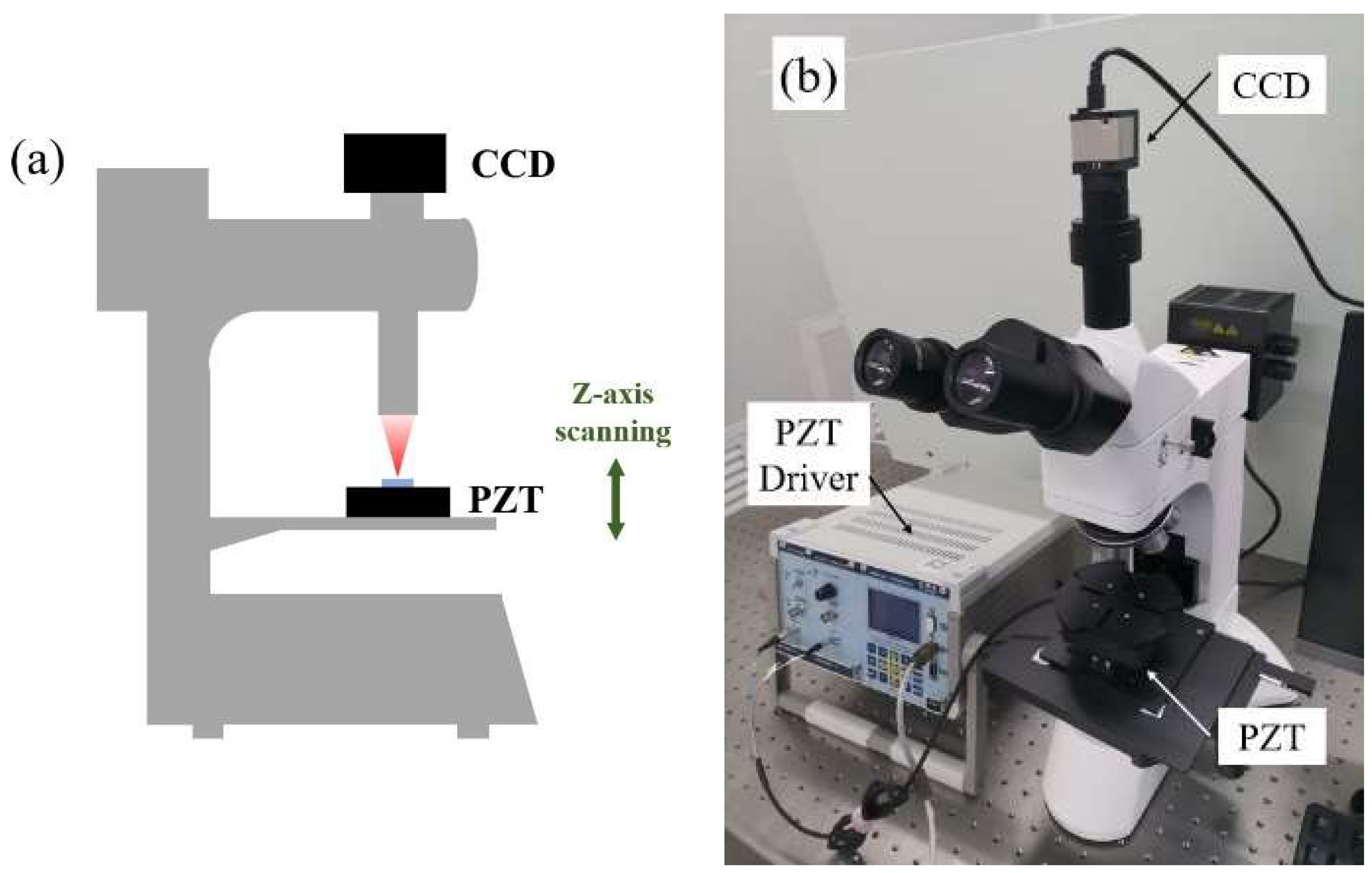
Figure 1. (a) Schematic and (b) photograph of TSOM setup. CCD, charge-coupled device; PZT, Piezoelectric Transducer.
Applsci 12 08396 g001
Figure 2. MEMS trench section diagram and its geometric parameters. W, width; D, depth.
Applsci 12 08396 g002
Figure 3. Process to construct a TSOM image.
Applsci 12 08396 g003
Figure 4. SEM images of MEMS HAR trench sections with width and depth of (a) 1.98 μm and 169 μm, (b) 10.3 μm and 321 μm, (c) 30.3 μm and 443 μm, (d) 30.3 μm and 37.3 μm, (e) 30.3μm and 131 μm, (f) 30.3 μm and 443 μm (inset: corresponding TSOM images).
Applsci 12 08396 g004
Figure 5. Process to collect TSOM image dataset.
Applsci 12 08396 g005
Figure 6. Schematic diagram of improved CNN model.
Applsci 12 08396 g006
Figure 7. Width and depth prediction results. Comparison between the actual (black triangles) and predicted (red circles) widths of HAR trenches with widths of around (a) 2 µm, (b) 10 µm, and (c) 30 µm; comparison between the actual (black triangles) and predicted (red circles) depths of HAR trenches with widths of (d) 1.93 µm, (e) 10.3 µm, and (f) 30.3 µm.
Applsci 12 08396 g007
Figure 8. Standard deviation and error of width results for widths around (a) 2 µm, (b) 10 µm, and (c) 30 µm, predicted by machine learning model (dot line) and deep learning model (solid line). ML, machine learning; DL, deep learning; SD, standard deviation.
Applsci 12 08396 g008
Figure 9. Standard deviation and error of depth results for widths of (a) 1.93 µm, (b) 10.3 µm, and (c) 30.3 µm, predicted by machine learning model (dot line) and deep learning model (solid line). ML, machine learning; DL, deep learning; SD, standard deviation.
Applsci 12 08396 g009
Publisher’s Note: MDPI stays neutral with regard to jurisdictional claims in published maps and institutional affiliations.