Article

Radiation Damage of Polydimethylsiloxane and Polyimide by X-ray Free-Electron Laser

1
Department of Mechanical Engineering, Pohang University of Science and Technology, Pohang 37673, Korea
2
Department of Materials Science and Engineering, Pohang University of Science and Technology, Pohang 37673, Korea
3
Department of Life Science, Pohang University of Science and Technology, Pohang 37673, Korea
4
Pohang Accelerator Laboratory, Pohang University of Science and Technology, Pohang 37673, Korea
5
Department of Chemical Engineering, Pohang University of Science and Technology, Pohang 37673, Korea
6
POSTECH Biotech Center, Pohang University of Science and Technology, Pohang 37673, Korea
*
Author to whom correspondence should be addressed.
Appl. Sci. 2022, 12(17), 8431; https://doi.org/10.3390/app12178431
Submission received: 1 August 2022 / Revised: 20 August 2022 / Accepted: 20 August 2022 / Published: 24 August 2022
(This article belongs to the Section Optics and Lasers)

Abstract

:

Featured Application

Our results provide insight into the material selection and directions to pursue in developing sample delivery devices used in XFEL studies.

Abstract

A crystal delivery system is essential in serial femtosecond crystallography experiments using an X-ray free-electron laser (XFEL). Investigating the XFEL-induced radiation damage to materials potentially applicable to sample delivery devices is vital for developing a sample delivery system. In this study, we investigated the radiation damage caused by an XFEL to polydimethylsiloxane (PDMS) and polyimide (PI), which are widely used as sample delivery materials in synchrotron X-rays. Upon XFEL exposure, the PDMS film produced irregularly shaped and sized holes, whereas the PI film produced relatively regular shaped and sized holes. When XFELs were exposed to the channel of the PDMS-based microfluidic device, holes were generated on the film by the radiation damage and the microfluidic device and the internal channel region were structurally destroyed. The PI-based microfluidic device experienced no structural destruction, except for the holes generated by the XFEL. However, as the XFELs were continuously exposed, bubbles generated from the solution due to radiation damage; the accumulation of these bubbles interfered with the path of the inner channel of the microfluidic device. Our results will not only help understand the phenomenon of radiation damage of PDMS and PI films by XFEL, but also provide insight into the directions to pursue in developing applications of PDMS and PI films in XFEL studies.

1. Introduction

X-ray free-electron lasers (XFELs) produce intense X-rays with ultrashort pulse widths, which are beneficial for understanding the time-resolved molecular dynamics ranging from small molecules to macromolecules [1]. The serial femtosecond crystallography (SFX) technique using XFEL allows for determining the room-temperature structure of small molecules or macromolecules while minimizing radiation damage [2,3,4,5]. In addition, SFX with pump-probe or mix-and-inject techniques enables the visualization of the time-resolved molecular dynamics of target molecules [6,7,8]. In SFX experiments, a sample delivery system is essential for continuously and reliably delivering the crystals to the X-ray interaction point [9,10,11]. Various sample delivery methods, such as injector [12,13,14], injector/syringe with viscous medium [11,15,16,17,18,19,20,21], fixed-target scanning [22,23,24,25,26,27,28], capillary methods [29,30], microfluidic devices [31,32,33,34], and hybrid methods of injection-and-transfer [35], have been developed and successfully applied in serial crystallography experiments. In SFX experiments, depending on the sample delivery approach, the crystal sample is directly exposed to the XFEL, or the crystal sample and sample delivery device are simultaneously exposed to the XFEL by enclosing or depositing the crystal sample in a film. The sample delivery method using an injector/syringe is a representative experimental method in which a crystal suspension (or crystals embedded in a viscous medium) is directly exposed to an XFEL. Among these, liquid jet injectors minimize X-ray background scattering by extruding an injection stream composed of a crystal suspension [12]. This system delivers the crystal suspension at a high flow rate to produce a stable injection stream, which is beneficial for applying the XFEL facility with a high repetition rate. Contrarily, when a liquid jet injector is applied to an XFEL facility with a low repetition rate, non-hit crystals are overwhelmingly wasted compared to crystals exposed to XFEL; therefore, this delivery method is inefficient in terms of sample consumption. An alternative is to embed the crystals in a viscous medium and deliver them at a low flow rate to maintain a stable injection stream [11,13,15,36]. However, crystals are often physically damaged during mixing with a viscous medium or dissolved by a chemical reaction between the crystals and viscous medium, which can impair the diffraction quality of the crystals [11]. Therefore, this method often requires effort to find a suitable viscous material depending on the crystal sample.
Another crystal delivery approach is to enclose or deposit the crystals using a polymer film or micro-patterned chips, such as the fixed-target scanning method [22,23,24,25,26,27] or a hybrid method such as drop-on-drop [35] or a combination of an inject-and-transfer system (BITS) [37]. In these methods, crystals are enclosed or deposited on a film and delivered to an X-ray interaction point using a programmed translation stage or conveyer approach. These methods have the advantage of lower sample consumption than the injector method [27]. In addition, these methods cause minimal physical damage to the crystals during sample delivery compared to the injector method [27]. In previous SFX experiments, polyimide (PI) films [25,27] and Mylar films [38] have been applied to deliver crystal samples using a fixed-target scanning approach or BITS system approach. When the XFEL penetrates the film, the XFEL radiation damage creates a hole in the film where the XFEL is transmitted. This indicates that radiation damage studies using XFEL are required in advance for attractive materials that can potentially be applied for developing SFX sample delivery devices.
Polydimethylsiloxane (PDMS) is a high-performance polymer with thermo-tolerance, resistance to oxidation, ease of fabrication, and tunable hardness [39]. The fundamental [–OSi(CH3)2–]n structure in PDMS has intrinsic hydrophobic properties [39]. The plasma immersion ion implantation technique can enhance the hydrophilicity and biocompatibility of PDMS [40]. PDMS is an inexpensive rubbery elastomer with excellent optical clarity [41]; it can be structured to any desired shape, thickness, and size using a soft lithography technique based on replication molding of micromachined molds [41]. Because of these advantages, PDMS has been widely used as a sample delivery material in X-ray research [42,43]. PI is a high-performance polymer with excellent temperature stability, solvent resistance, radiation resistance, and mechanical strength [44,45]. Because PI produces considerably low background scattering when exposed to X-rays [25], which does not affect data processing, it has been widely used as a sample delivery material in serial crystallography (SX) studies [34,46,47] and for crystal mounting loops in macromolecular crystallography [48].
In this study, we investigate the radiation damage to PDMS and PI caused by XFEL. We analyze the radiation damage to films and microfluidic devices exposed to XFEL. Our results expand our knowledge of XFEL-induced radiation damage and provide insight into the direction of the development of sample delivery systems for SFX experiments and XFEL science.

2. Materials and Methods

2.1. Materials

PDMS was purchased from Dow Corning (Slygard 184, United States). The PDMS film was manufactured via treatment with trichloro(1H,1H,2H,2H-perfluorooctyl)silane, as previously reported [49]. The PI film (25 μm) was purchased from Covalue Youngjin Co. (Daegu, Korea). The PDMS-based microfluidic device was fabricated using previously reported conventional soft lithography procedures [50]. The width and height of the channel in the PDMS-based microfluidic device were 100 μm and ~30 μm, respectively. The PI-based microfluidic device was fabricated by assembling PI films as previously reported [51]. The width and height of the PI-based microfluidic device were 500 μm and 100 μm, respectively.

2.2. Measurement of Background Scattering

The X-ray scattering of PDMS (20 and 90 μm) and PI (25 μm) using synchrotron X-rays was measured at the 5C or 11C beamline at the Pohang Accelerator Laboratory (PLS-II, Pohang, Korea). The X-ray energy and photon flux were 12.4 keV and ~1 × 10¹²/s, respectively. The PDMS or PI films were exposed to X-rays for 100 ms. The X-ray background scattering was recorded using a Eiger 9M or PILATUS 6M detector. The X-ray background scattering was visualized and analyzed using ADXV (https://www.scripps.edu/tainer/arvai/adxv.html) (accessed on 19 August 2022).

2.3. Radiation Damage of PDMS and PI by XFEL

Radiation damage of PDMS and PI by the XFEL was performed at the nano-crystallography and coherent imaging (NCI) hutch [52] at the Pohang Accelerator Laboratory X-ray Free-Electron Laser (PAL-XFEL) [53]. The XFEL energy and photon flux were 9.5 keV and ~5 × 10¹¹phs/pulse, respectively. The beam had a size of approximately 3 μm × 2 μm (vertical × horizontal: FWHM) and was focused by the Kirkpatrick–Baez mirror [54]. The repetition rate of the XFEL used in this experiment was 30 Hz. In the study of radiation damage using PDMS or PI film, the film was mounted on a two-dimensional (2D) manipulator inside a fixed target chamber, and raster-scanned in the vertical and horizontal directions. The XFEL exposure interval during raster scanning was 50 μm in both vertical and horizontal directions. In an experiment to monitor radiation damage in real time, the XFEL was continuously exposed at one location, and this was recorded using a high-speed camera (IDP-Express R2000, Photron, Japan). When exposing PDMS and PI based microfluidics to the XFEL, one position on the microfluidic channel was continuously exposed. All the XFEL experiments were performed at room temperature (24–26 °C) in ambient air.

3. Results

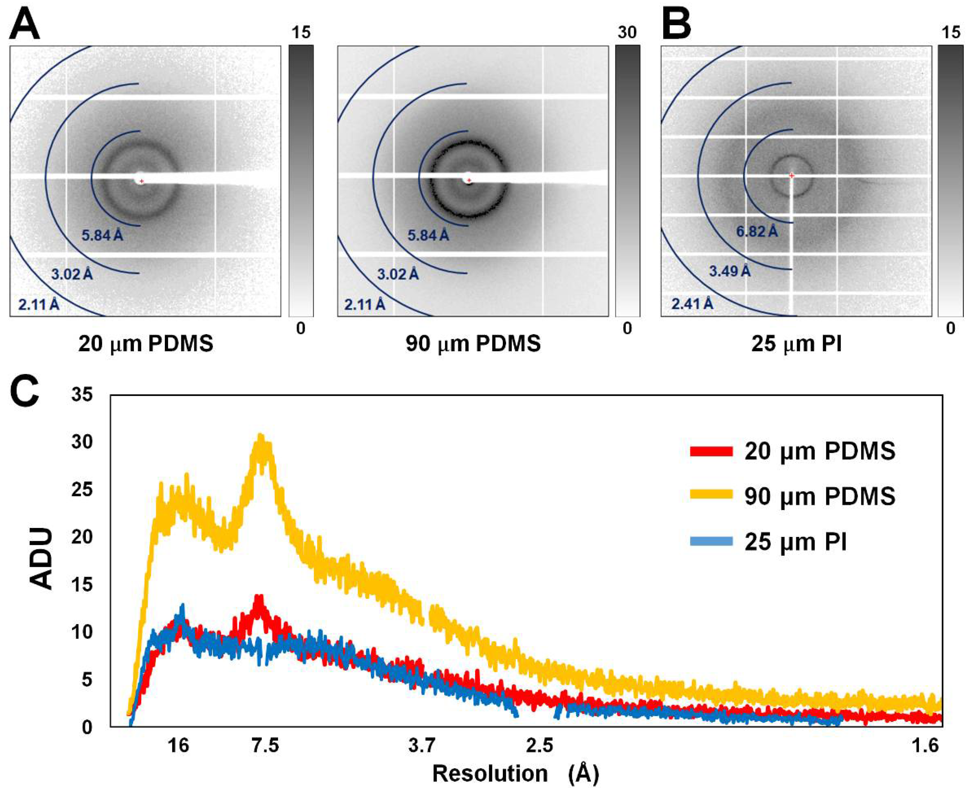
3.1. X-ray Scattering Background of PDMS and PI

When microcrystals are enclosed or deposited on a film and exposed to XFEL, diffraction from the crystal sample and X-ray background scattering from the film occur [25]. X-ray background scattering from the film is noise, which affects the signal-to-noise ratio (SNR) of the signal from the target molecule [25]. Therefore, the quality of the PDMS and PI films with low X-ray background scattering is vital. To check the use of the PDMS and PI films, we investigated X-ray background scattering of the PDMS and PI used in this experiment. We first attempted to investigate the X-ray scattering of PDMS and PI by exposing them to an XFEL. However, images acquired during the experiment showed a high background noise, with or without the film, indicating that noise was generated from the XFEL used in the experiment and the experimental environment. Accordingly, the scattering of the film using the XFEL could not be accurately validated; therefore, we checked the quality of the films using synchrotron X-rays. We measured the X-ray scattering of PDMS with various thicknesses (20 and 90 μm) and PI (25 μm) by exposing them to X-rays for 100 ms (Figure 1). The X-ray background scattering of PDMS was observed around 7.5 Å and 16 Å (Figure 1A). When the X-ray exposure time was 100 ms, the 20 and 90 μm-thicknesses of PDMS films had analogue-to-digital units (ADU) values of 12.1/12.7 and 26.3/30.8, respectively, at a scattering area of 7.5/16 Å. The X-ray background scattering of PI was observed at approximately 15 Å (Figure 1B). When the X-ray exposure time was 100 ms, the 25 μm-thickness of the PI film had ADU values of 11.6. The background scattering of the films used in this experiment is negligible when analyzing the diffraction signals (Figure 1C). After X-ray exposure, the PDMS and PI films were not damaged by synchrotron X-rays. Therefore, these two polymer films can be reused at synchrotron X-rays, as in previous synchrotron applications.

3.2. Radiation Damage of PDMS and PI by XFEL

In the SFX experiment, the polymer film can be used as an enclosing film to prevent dehydration of the crystal suspension in a fixed-target sample holder [25,27] or as a support for crystals in the BITS system [37]. In both sample delivery approaches, crystals on polymer films are raster scanned to the XFEL in both the vertical and horizontal directions, according to the motion of the translation stage. To better understand the phenomenon of XFEL-induced radiation damage during data collection, PDMS and PI films were raster scanned in both the vertical and horizontal directions during XFEL exposure. During raster scanning, the scanning interval was 50 μm; therefore, the XFEL exposure position did not affect the next XFEL exposure position based on the XFEL beam size (calculated full size of XFEL: <8 μm). In the real-time monitoring, in the case of the PDMS film, radiation damage was observed by a clearly visible brightness change in the part through which the XFEL was transmitted (Figure 2A and Supplementary Video S1). For the PI film, no notable phenomena that could be considered radiation damage were observed during raster scanning on a real-time monitor (Figure 2B and Supplementary Video S2); however, actual radiation damage occurred (see below).
Furthermore, the XFEL-exposed films were analyzed using high-resolution microscopy. In both films used in the experiment, holes due to radiation damage were commonly generated in the positions through which the XFEL transmitted, indicating that the XFEL fluences exceeded the damage threshold of both materials. Meanwhile, the physical phenomena for radiation-damaged holes on PDMS and PI films were different. For the PDMS film, the shape of the hole generated by the XFEL radiation damage varied, and the hole size was 15–40 μm, which is 5–20 times larger than that of the XFEL beam (FWHM) used in the experiment (Figure 2C). For the PI film, a crater-like hole formed in the transmission area of the XFEL beam, and the size of the hole due to radiation damage was 3 and 2 μm in the vertical and horizontal directions, respectively, similar to the FWHM size of the focused XFEL beam (Figure 2D). In addition, approximately 2–4 μm of the film around the hole was depressed, and the total size of the depressed area was similar to the full size of the XFEL beam (Figure 2D). These depressions appeared to have been melted by XFEL exposure. The hole pattern on the PI film in this experiment is similar to the pattern shown in the PI film for enclosing the crystals in the sample holder in the previous fixed-target SFX experiment [25,27].

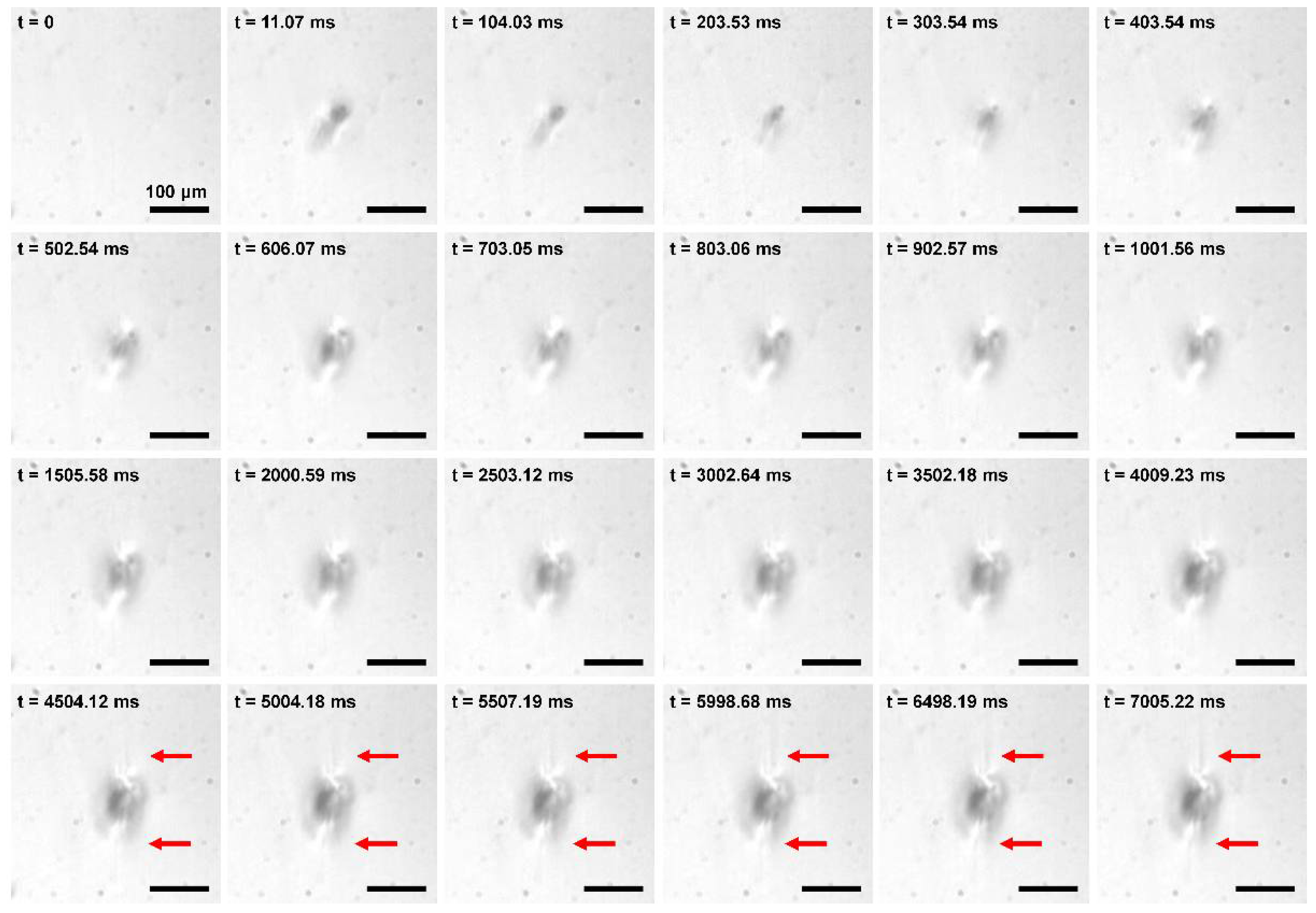
3.3. Time-Lapse Observation of the Radiation Damage of PDMS and PI

We analyzed the radiation damage using a high-speed camera to observe how the PDMS film was physically damaged over time when continuously exposed to XFEL. When the PDMS was continuously exposed to XFEL, the hole in the film continued to enlarge, particularly in the vertical direction (Figure 3 and Supplementary Video S3). Because the pulse width of the XFEL was ~20 fs, physical radiation damage must have occurred in the PDMS or PI film immediately after the XFEL beam was transmitted. In our experimental system, the exact destruction time of the PDMS film was not defined owing to the limitation of the camera specifications and experimental setup. Nevertheless, we observed the phenomenon of radiation damage of the PDMS film that the size of the hole at the point where the XFEL is transmitted gradually increased. After approximately 4 s, we observed formation of linear features extending vertically above and below the beam transmission area (Figure 3). The apparent difference in focus of the camera on the hole, even though taken at the same location, is considered to be due to the deformation of the PDMS film in the XFEL-exposed area (see Discussion). Overall, we observed that when the PDMS was continuously exposed to XFEL, with time, the hole in the film increased centered on the point where the XFEL was transmitted through, and structural deformation occurred.

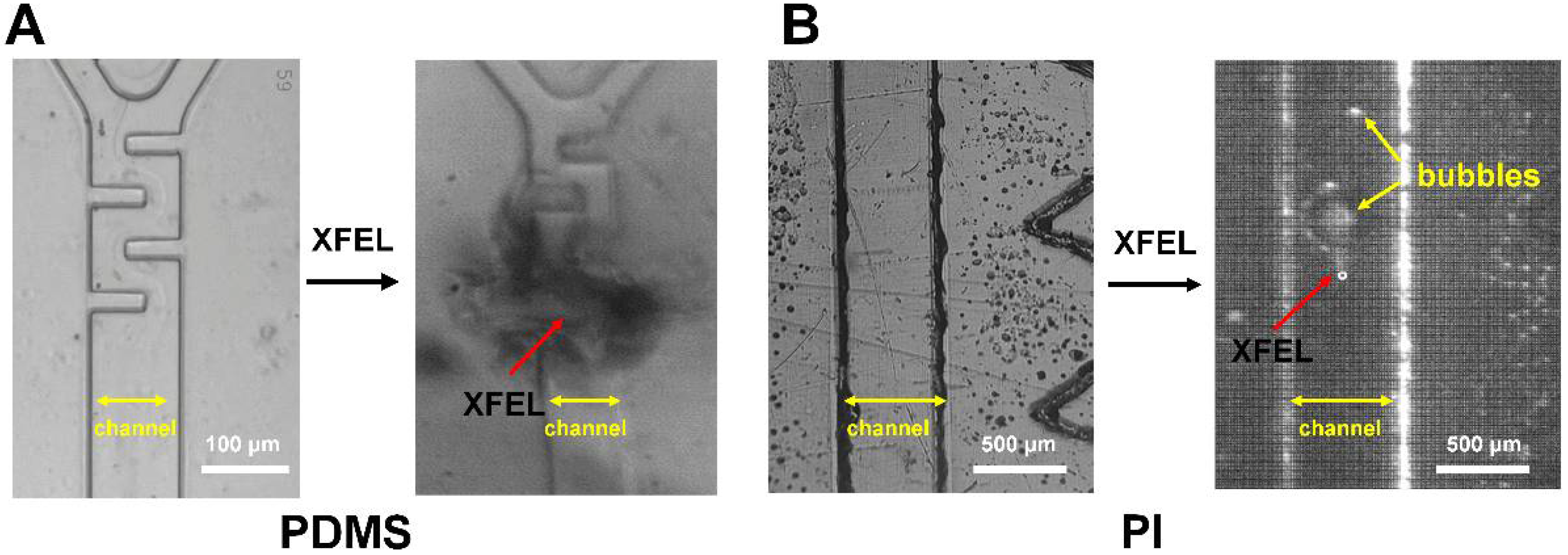
3.4. Observation of Radiation Damage on PDMS- and PI-Based Microfluidics Chips

The SFX with the mix-and-inject technique is significant for elucidating the time-resolved molecular mechanism for interactions (or reactions) between the substrate (or inhibitor) and macromolecule crystals [55]. Various mix-and-inject systems have been developed, such as the injector [56,57,58] and conveyer belt [35] approach. Among them, the microfluidic method has been developed for time-resolved SX using synchrotron X-rays [32]. The advantage of this method is that the crystals and ligand solutions are mixed in the channel and precisely exposed to X-rays at the desired time. In addition, as in the sample delivery method using capillaries [30] or single-channel microfluidics [34], all samples pass through the inner channel aligned with the X-ray. In a previous serial synchrotron crystallography (SSX) experiment, synchrotron X-rays directed onto a microfluidic device made of PI, and no physical radiation damage was observed on the device [32]. Meanwhile, in the XFEL experiment, there has been no report of a case in which diffraction data were collected by directly exposing the microfluidic chip channel. Based on our results for XFEL-induced radiation damage on PDMS and PI films, we believed that a microfluidic device made of PDMS and PI would potentially be physically damaged at the position of XFEL penetration. We expected the occurrence of large holes in PDMS-based microfluidics and leakage of crystals or solutions. In PI-based microfluidic devices, holes may occur in the channel area through which the XFEL passes; however, the hole size is small. Therefore, we expected that, due to surface tension, no leakage of the solution or crystals would occur.
To demonstrate our hypothesis, we exposed a microfluidic device fabricated using PDMS and PI to XFELs during the flow of the solution. When a PDMS-based microfluidic chip was exposed to XFEL, a large hole (>100 μm) was created at the XFEL penetration position, as for the PDMS film (Figure 4A). Moreover, we observed physical and structural distortions of the PDMS-based microfluidic device. Accordingly, the solution did leak out from the hole generated by the XFEL radiation damage in the microfluidic device. Consequently, the PDMS-based microfluidic device is considered to have no application in XFEL experiments where the material is exposed to the XFEL.
For PI-based microfluidics, a hole was generated in the area through which the XFEL passed (Figure 4B). However, in the PI-based microfluidic device, unlike in the PDMS microfluidic chip, the flowing solution in the channel did not exit the hole generated by the XFEL. Instead, bubbles owing to radiation damage formed at the point exposed to XFEL (Figure 4B and Supplementary Video S4). Upon exposure to XFEL, these bubbles formed continuously and moved through the channel in the opposite direction to gravity, changing the flow path of the solution at the top. Continuous small bubbles accumulated to form large bubbles in the inner channel of the microfluidic device, and eventually, large bubbles were trapped inside the channel of the microfluidic device (Figure 4B and Supplementary Video S4). As these bubbles did not cover the entire area inside the channel, they were not washed out by the flowing solution. Consequently, these bubbles interfered with the path of the solution or crystal sample. This will be applicable for delivering solutions or crystal samples used in typical X-ray diffraction or scattering experiments. For performing a time-resolved SFX experiment with a mix-and-inject approach using microfluidics, the issue arises of microcrystals not being delivered at the desired time, owing to the change in the sample path.

4. Discussion

In SFX experiments, a sample delivery device is necessary. Among various sample delivery devices, a polymer film is often used as a material for the sample delivery device. To expand our knowledge about radiation damage of polymer films for XFEL and understand their potential applications, we investigated the XFEL-induced radiation damage of PDMS and PI materials, which are widely used as materials for sample delivery devices in synchrotron X-ray research due to their lack of radiation damage. Upon irradiation with XFEL, both PDMS and PI materials were physically damaged, resulting in holes in the film at the position penetrated by XFEL; however, the pattern of holes generated by XFEL radiation damage differed between the PDMS and PI films. The XFEL-exposed PDMS film exhibited holes of various sizes and shapes. Consequently, the shape of the hole caused by physical radiation damage in the PDMS film exposed to the XFEL was not consistent with the shape of each XFEL-exposed point. In particular, because the size of the hole was significantly larger than the size of the beam, it temporarily affected the surrounding sample when scanning at short intervals in the raster scanning experiment. Meanwhile, the XFEL-induced holes on the PI film showed relatively similar sized and shaped holes compared to the PDMS film.
Overall, the patterns of holes generated by physical radiation damage varied across all types of films exposed to XFEL. We consider three possibilities as to why each shot on the film causes different levels of radiation damage: (1) Because the X-ray intensity of a natural XFEL pulse varies from shot to shot, radiation damage patterns in the holes of PDMS and PI films cannot be identical. Considering the natural characteristics of the XFEL pulses, the difference in the size and shape of holes observed in the PI film can be attributed to the XFEL energy fluctuation. (2) Depending on the uniformity and thickness of the film, the effect of physical radiation damage on the film may differ when exposed to an XFEL. If the XFEL exposes a film with a uniform interior and surface, the pattern of the generated hole will be similar; however, the physical radiation damage in PDMS is quite variable. In addition, the physical impact will vary depending on the thickness of the film; the thinner the film, the more the radiation damage is restricted to the part through which the XFEL is transmitted. Overall, because the PDMS film used in this experiment was directly processed and manufactured, we assume that its uniformity was lower than that of the commercially processed PI film. (3) The physical radiation damage differs according to the intrinsic properties of the film material. The PDMS and PI films used in this experiment differed in various physical properties, such as material composition, structure, strength, X-ray absorption, and thermal stability. For example, Koyama et al. used a 1 μm-focused XFEL beam to investigate the ablation thresholds of optical materials [59]. When optical materials are exposed to an XFEL, the imprint area generated on their surfaces varies depending on the energy exposed and for each material. The measured threshold fluences of the uncoated Si, uncoated SiO2, Si under a Pt coating layer, SiO2 under a Pt coating layer, Pt, and Rh were 0.78 ± 0.04, 4.5 ± 0.7, 0.065 ± 0.008, 0.11 ± 0.03, 0.023 ± 0.004, and 0.072 ± 0.007 μJ/μm2, respectively [59]. Accordingly, even if the PDMS and PI materials have the same uniformity and thickness, the physical damage caused by exposure to the XFEL will differ. Consequently, we believe that the physical radiation damage between PDMS and PI differs from shot to shot and is caused by the difference in the characteristics of the XFEL, the uniformity of the materials, and the physical properties of the two materials. Accordingly, we expect that the radiation damage pattern that appears when a different type of film is exposed to an XFEL will differ depending on the material and XFEL characteristics.
Because of the large hole size of the PDMS film due to its exposure to the XFEL, raster scanning in FT-SFX may be limited to wide intervals. However, in the case of a PI film, the sample consumption can be reduced by scanning more narrowly than the 50 μm interval used in the experiment. Nevertheless, PDMS can be easily and freely processed in the laboratory to any desired size, thickness, or design. For PDMS application in SFX, to minimize the physical radiation damage of the PDMS film exposed to XFEL, it is critical not only to make the PDMS film more uniform but also to make it significantly thin.
We observed radiation damage by continuously exposing the PDMS and PI films to the XFEL. When the XFEL was continuously passed through the PDMS film, the size of the hole gradually increased after the hole was generated at the point where the XFEL penetrated; physical damage, considered radiation damage, was also observed in the film area around the hole. Observing this with a high-speed camera, we confirmed that the focus of the hole changed as shown in Supplementary Video S3, which tentatively indicates that the film around the PDMS hole moved fluidly when the XFEL was continuously exposed. Because the position jitter of the XFEL beam used in the experiment was <1 µm per day, the gradual increase in the hole after the penetration of the XFEL in PDMS was unaffected by the movement of the main beam. Accordingly, it is considered physical damage to the PDMS chip owing to the continuous exposure of the parasitic scattering around the focused beam. Contrarily, in the PI film, no significant change occurred in the hole size after the XFEL passed through holes despite continuous exposure. We believe that the parasitic scattering around the main XFEL beam cannot affect the PI film.
In a microfluidic device based on PDMS and PI, we observed unique radiation damage when the XFEL passed through the inner channel through which the sample passed. In PDMS-based microfluidics, not only the occurrence of holes due to radiation damage was observed in the PI film, but also the structural distortion of the PDMS device around the inner channel to which the XFEL was continuously exposed was observed. In addition, we observed that the solution sample delivered to the inner channel leaked through the large hole generated in the PDMS microfluidic device. Consequently, collecting diffraction data while penetrating the XFEL through the inner channel of the PDMS-based microfluidic chip is considered impossible. Contrarily, in the PI-based microfluidics chip, holes were generated by XFEL penetration; however, structural destruction of the microfluidic device was not observed, even when the XFEL was continuously exposed. Meanwhile, the solution did not leak from the holes created in the PI microfluidic device. As the internal pressure is higher than the atmospheric pressure, leaking can occur in terms of pressure. However, we assume that there is no leakage into the small hole of the solution owing to the surface tension of the solution.
However, when the XFEL penetrates the inner channel of PI microfluidics, the inner channel is partially blocked by bubbles caused by radiation damage to the solution, and there is an issue of changing the route of the solution flowing through it. To solve this issue, the sample flow rate can be temporarily increased to expel air bubbles out of the channel; however, this has the disadvantage of increasing sample consumption. Consequently, we concluded that exposing the inner channel of a microfluidic device to an XFEL and collecting data has a tentative experimental limit due to radiation damage.

5. Conclusions

Here, we observed the radiation damage occurring when PDMS films, PI films, and microfluidic devices are exposed to XFEL. Unlike synchrotron X-rays, XFEL causes severe physical damage to PDMS and PI films. The findings of this study provide beneficial information for developing sample delivery devices for future SFX and XFEL research.

Supplementary Materials

The following supporting information can be downloaded at: https://www.mdpi.com/article/10.3390/app12178431/s1, Video S1: Raster scanning of PDMS film on the XFEL exposure; Video S2: Raster scanning of PI film on the XFEL exposure; Video S3: Real-time monitoring of XFEL-induced radiation damage of PDMS film; Video S4: Bubbles generated radiation damage in PI-based microfluidic devices.

Author Contributions

Conceptualization, K.L., D.L., W.K.C. and Y.C.; Methodology, K.L., D.L. and S.B.; Formal Analysis, K.L., J.K. (Jangwoo Kim), and K.H.N.; Investigation, K.L., D.L., J.K. (Jangwoo Kim) and K.H.N.; Resources, J.-L.L., W.K.C. and Y.C.; Data Curation, K.L., D.L., J.K. (Jihan Kim), J.P., S.J.L., S.P., Y.C. and K.H.N.; Writing, K.H.N.; Visualization, K.L. and K.H.N.; Funding Acquisition, Y.C. and K.H.N. All authors have read and agreed to the published version of the manuscript.

Funding

This work was funded by the National Research Foundation of Korea (NRF) (NRF-2017M3A9F6029736; NRF-2020M3H1A1075314; NRF-2021R1I1A1A01050838).

Institutional Review Board Statement

Not applicable.

Informed Consent Statement

Not applicable.

Data Availability Statement

Not applicable.

Acknowledgments

We would like to thank the beamline staff at NCI beamline at PAL-XFEL for their assistance with data collection (proposal Nos. 2021-2nd-NCI-013 and 2022-1st-NCI-015).

Conflicts of Interest

The authors declare no conflict of interest.

References

  1. Nam, K.H. Molecular dynamics-From small molecules to macromolecules. Int. J. Mol. Sci. 2021, 22, 3761. [Google Scholar] [CrossRef] [PubMed]
  2. Chapman, H.N.; Fromme, P.; Barty, A.; White, T.A.; Kirian, R.A.; Aquila, A.; Hunter, M.S.; Schulz, J.; DePonte, D.P.; Weierstall, U.; et al. Femtosecond X-ray protein nanocrystallography. Nature 2011, 470, 73–77. [Google Scholar] [CrossRef] [PubMed]
  3. Boutet, S.; Lomb, L.; Williams, G.J.; Barends, T.R.; Aquila, A.; Doak, R.B.; Weierstall, U.; DePonte, D.P.; Steinbrener, J.; Shoeman, R.L.; et al. High-resolution protein structure determination by serial femtosecond crystallography. Science 2012, 337, 362–364. [Google Scholar] [CrossRef] [Green Version]
  4. Durdagi, S.; Dag, C.; Dogan, B.; Yigin, M.; Avsar, T.; Buyukdag, C.; Erol, I.; Ertem, F.B.; Calis, S.; Yildirim, G.; et al. Near-physiological-temperature serial crystallography reveals conformations of SARS-CoV-2 main protease active site for improved drug repurposing. Structure 2021, 29, 1382–1396. [Google Scholar] [CrossRef] [PubMed]
  5. Nam, K.H. Room-temperature structure of xylitol-bound glucose isomerase by serial crystallography: Xylitol binding in the M1 site induces release of metal bound in the M2 site. Int. J. Mol. Sci. 2021, 22, 3892. [Google Scholar] [CrossRef]
  6. Tenboer, J.; Basu, S.; Zatsepin, N.; Pande, K.; Milathianaki, D.; Frank, M.; Hunter, M.; Boutet, S.; Williams, G.J.; Koglin, J.E.; et al. Time-resolved serial crystallography captures high-resolution intermediates of photoactive yellow protein. Science 2014, 346, 1242–1246. [Google Scholar] [CrossRef] [Green Version]
  7. Schmidt, M. Time-resolved macromolecular crystallography at pulsed X-ray sources. Int. J. Mol. Sci. 2019, 20, 1401. [Google Scholar] [CrossRef] [Green Version]
  8. Pandey, S.; Bean, R.; Sato, T.; Poudyal, I.; Bielecki, J.; Cruz Villarreal, J.; Yefanov, O.; Mariani, V.; White, T.A.; Kupitz, C.; et al. Time-resolved serial femtosecond crystallography at the European XFEL. Nat. Methods 2020, 17, 73–78. [Google Scholar] [CrossRef]
  9. Grünbein, M.L.; Nass Kovacs, G. Sample delivery for serial crystallography at free-electron lasers and synchrotrons. Acta Crystallogr. D Biol. Crystallogr. 2019, 75, 178–191. [Google Scholar] [CrossRef]
  10. Zhao, F.Z.; Zhang, B.; Yan, E.K.; Sun, B.; Wang, Z.J.; He, J.H.; Yin, D.C. A guide to sample delivery systems for serial crystallography. FEBS J. 2019, 286, 4402–4417. [Google Scholar] [CrossRef] [Green Version]
  11. Nam, K.H. Sample delivery media for serial crystallography. Int. J. Mol. Sci. 2019, 20, 1094. [Google Scholar] [CrossRef] [PubMed] [Green Version]
  12. DePonte, D.P.; Weierstall, U.; Schmidt, K.; Warner, J.; Starodub, D.; Spence, J.C.H.; Doak, R.B. Gas dynamic virtual nozzle for generation of microscopic droplet streams. J. Phys. D 2008, 41, 195505. [Google Scholar] [CrossRef] [Green Version]
  13. Weierstall, U.; James, D.; Wang, C.; White, T.A.; Wang, D.; Liu, W.; Spence, J.C.; Bruce Doak, R.; Nelson, G.; Fromme, P.; et al. Lipidic cubic phase injector facilitates membrane protein serial femtosecond crystallography. Nat. Commun. 2014, 5, 3309. [Google Scholar] [CrossRef] [PubMed] [Green Version]
  14. Vakili, M.; Vasireddi, R.; Gwozdz, P.V.; Monteiro, D.C.F.; Heymann, M.; Blick, R.H.; Trebbin, M. Microfluidic polyimide gas dynamic virtual nozzles for serial crystallography. Rev. Sci. Instrum. 2020, 91, 085108. [Google Scholar] [CrossRef]
  15. Sugahara, M.; Mizohata, E.; Nango, E.; Suzuki, M.; Tanaka, T.; Masudala, T.; Tanaka, R.; Shimamura, T.; Tanaka, Y.; Suno, C.; et al. Grease matrix as a versatile carrier of proteins for serial crystallography. Nat. Methods 2015, 12, 61–63. [Google Scholar] [CrossRef] [Green Version]
  16. Berntsen, P.; Hadian Jazi, M.; Kusel, M.; Martin, A.V.; Ericsson, T.; Call, M.J.; Trenker, R.; Roque, F.G.; Darmanin, C.; Abbey, B. The serial millisecond crystallography instrument at the Australian Synchrotron incorporating the “Lipidico” injector. Rev. Sci. Instrum. 2019, 90, 085110. [Google Scholar] [CrossRef]
  17. Park, S.Y.; Nam, K.H. Sample delivery using viscous media, a syringe and a syringe pump for serial crystallography. J. Synchrotron Radiat. 2019, 26, 1815–1819. [Google Scholar] [CrossRef] [Green Version]
  18. Nam, K.H. Polysaccharide-based injection matrix for serial crystallography. Int. J. Mol. Sci. 2020, 21, 3332. [Google Scholar] [CrossRef]
  19. Nam, K.H. Shortening injection matrix for serial crystallography. Sci. Rep. 2020, 10, 107. [Google Scholar] [CrossRef] [Green Version]
  20. Nam, K.H. Lard injection matrix for serial crystallography. Int. J. Mol. Sci. 2020, 21, 5977. [Google Scholar] [CrossRef]
  21. Nam, K.H. Beef tallow injection matrix for serial crystallography. Sci. Rep. 2022, 12, 694. [Google Scholar] [CrossRef] [PubMed]
  22. Hunter, M.S.; Segelke, B.; Messerschmidt, M.; Williams, G.J.; Zatsepin, N.A.; Barty, A.; Benner, W.H.; Carlson, D.B.; Coleman, M.; Graf, A.; et al. Fixed-target protein serial microcrystallography with an x-ray free electron laser. Sci. Rep. 2014, 4, 6026. [Google Scholar] [CrossRef] [PubMed] [Green Version]
  23. Cohen, A.E.; Soltis, S.M.; Gonzalez, A.; Aguila, L.; Alonso-Mori, R.; Barnes, C.O.; Baxter, E.L.; Brehmer, W.; Brewster, A.S.; Brunger, A.T.; et al. Goniometer-based femtosecond crystallography with X-ray free electron lasers. Proc. Natl. Acad. Sci. USA 2014, 111, 17122–17127. [Google Scholar] [CrossRef] [Green Version]
  24. Mueller, C.; Marx, A.; Epp, S.W.; Zhong, Y.; Kuo, A.; Balo, A.R.; Soman, J.; Schotte, F.; Lemke, H.T.; Owen, R.L.; et al. Fixed target matrix for femtosecond time-resolved and in situ serial micro-crystallography. Struct. Dyn. 2015, 2, 054302. [Google Scholar] [CrossRef] [PubMed] [Green Version]
  25. Lee, D.; Baek, S.; Park, J.; Lee, K.; Kim, J.; Lee, S.J.; Chung, W.K.; Lee, J.L.; Cho, Y.; Nam, K.H. Nylon mesh-based sample holder for fixed-target serial femtosecond crystallography. Sci. Rep. 2019, 9, 6971. [Google Scholar] [CrossRef] [Green Version]
  26. Tolstikova, A.; Levantino, M.; Yefanov, O.; Hennicke, V.; Fischer, P.; Meyer, J.; Mozzanica, A.; Redford, S.; Crosas, E.; Opara, N.L.; et al. 1 kHz fixed-target serial crystallography using a multilayer monochromator and an integrating pixel detector. IUCrJ 2019, 6, 927–937. [Google Scholar] [CrossRef]
  27. Lee, K.; Lee, D.; Baek, S.; Park, J.; Lee, S.J.; Park, S.; Chung, W.K.; Lee, J.L.; Cho, H.S.; Cho, Y.; et al. Viscous-medium-based crystal support in a sample holder for fixed-target serial femtosecond crystallography. J. Appl. Crystallogr. 2020, 53, 1051–1059. [Google Scholar] [CrossRef]
  28. Lee, D.; Park, S.; Lee, K.; Kim, J.; Park, G.; Nam, K.H.; Baek, S.; Chung, W.K.; Lee, J.L.; Cho, Y.; et al. Application of a high-throughput microcrystal delivery system to serial femtosecond crystallography. J. Appl. Crystallogr. 2020, 53, 477–485. [Google Scholar] [CrossRef] [Green Version]
  29. Stellato, F.; Oberthur, D.; Liang, M.; Bean, R.; Gati, C.; Yefanov, O.; Barty, A.; Burkhardt, A.; Fischer, P.; Galli, L.; et al. Room-temperature macromolecular serial crystallography using synchrotron radiation. IUCrJ 2014, 1, 204–212. [Google Scholar] [CrossRef]
  30. Nam, K.H. Stable sample delivery in viscous media via a capillary for serial crystallography. J. Appl. Crystallogr. 2020, 53, 45–50. [Google Scholar] [CrossRef]
  31. Monteiro, D.C.F.; Vakili, M.; Harich, J.; Sztucki, M.; Meier, S.M.; Horrell, S.; Josts, I.; Trebbin, M. A microfluidic flow-focusing device for low sample consumption serial synchrotron crystallography experiments in liquid flow. J. Synchrotron Radiat. 2019, 26, 406–412. [Google Scholar] [CrossRef] [PubMed]
  32. Monteiro, D.C.F.; von Stetten, D.; Stohrer, C.; Sans, M.; Pearson, A.R.; Santoni, G.; van der Linden, P.; Trebbin, M. 3D-MiXD: 3D-printed X-ray-compatible microfluidic devices for rapid, low-consumption serial synchrotron crystallography data collection in flow. IUCrJ 2020, 7, 207–219. [Google Scholar] [CrossRef] [PubMed] [Green Version]
  33. Echelmeier, A.; Cruz Villarreal, J.; Messerschmidt, M.; Kim, D.; Coe, J.D.; Thifault, D.; Botha, S.; Egatz-Gomez, A.; Gandhi, S.; Brehm, G.; et al. Segmented flow generator for serial crystallography at the European X-ray free electron laser. Nat. Commun. 2020, 11, 4511. [Google Scholar] [CrossRef]
  34. Nam, K.H.; Cho, Y. Stable sample delivery in a viscous medium via a polyimide-based single-channel microfluidic chip for serial crystallography. J. Appl. Crystallogr. 2021, 54, 1081–1087. [Google Scholar] [CrossRef]
  35. Butryn, A.; Simon, P.S.; Aller, P.; Hinchliffe, P.; Massad, R.N.; Leen, G.; Tooke, C.L.; Bogacz, I.; Kim, I.S.; Bhowmick, A.; et al. An on-demand, drop-on-drop method for studying enzyme catalysis by serial crystallography. Nat. Commun. 2021, 12, 4461. [Google Scholar] [CrossRef] [PubMed]
  36. Conrad, C.E.; Basu, S.; James, D.; Wang, D.; Schaffer, A.; Roy-Chowdhury, S.; Zatsepin, N.A.; Aquila, A.; Coe, J.; Gati, C.; et al. A novel inert crystal delivery medium for serial femtosecond crystallography. IUCrJ 2015, 2, 421–430. [Google Scholar] [CrossRef]
  37. Lee, K.; Kim, J.; Baek, S.; Park, J.; Park, S.; Lee, J.-L.; Chung, W.K.; Cho, Y.; Nam, K.H. Combination of an inject-and-transfer system for serial femtosecond crystallography. J. Appl. Crystallogr. 2022, 55, 813–822. [Google Scholar] [CrossRef]
  38. Doak, R.B.; Nass Kovacs, G.; Gorel, A.; Foucar, L.; Barends, T.R.M.; Grunbein, M.L.; Hilpert, M.; Kloos, M.; Roome, C.M.; Shoeman, R.L.; et al. Crystallography on a chip—Without the chip: Sheet-on-sheet sandwich. Acta Crystallogr. D Struct. Biol. 2018, 74, 1000–1007. [Google Scholar] [CrossRef]
  39. Jothi, L.; Nageswaran, G. Plasma modified polymeric materials for biosensors/biodevice applications. In Non-Thermal Plasma Technology for Polymeric Materials; Elsevier: Amsterdam, The Netherlands, 2019; pp. 409–437. [Google Scholar]
  40. Tong, L.; Zhou, W.; Zhao, Y.; Yu, X.; Wang, H.; Chu, P.K. Enhanced cytocompatibility and reduced genotoxicity of polydimethylsiloxane modified by plasma immersion ion implantation. Colloids Surf. B Biointerfaces 2016, 148, 139–146. [Google Scholar] [CrossRef]
  41. Haeberle, S.; Zengerle, R. Microfluidic for Lab-on-a-Chip. In Comprehensive Microsystems; Elesevier Science: Amsterdam, The Netherlands, 2008; pp. 463–516. [Google Scholar]
  42. Trebbin, M.; Krüger, K.; DePonte, D.; Roth, S.V.; Chapman, H.N.; Förster, S. Microfluidic liquid jet system with compatibility for atmospheric and high-vacuum conditions. Lab Chip 2014, 14, 1733–1745. [Google Scholar] [CrossRef]
  43. He, T.; Wang, C.; Urisu, T.; Nagahiro, T.; Tero, R.; Xia, R. The PDMS-based microfluidic channel fabricated by synchrotron radiation stimulated etching. Opt. Express 2010, 18, 9733–9738. [Google Scholar] [CrossRef] [PubMed]
  44. Sezer Hicyilmaz, A.; Celik Bedeloglu, A. Applications of polyimide coatings: A review. SN Appl. Sci. 2021, 3, 363. [Google Scholar] [CrossRef]
  45. Constantin, C.P.; Aflori, M.; Damian, R.F.; Rusu, R.D. Biocompatibility of polyimides: A mini-review. Materials 2019, 12, 3166. [Google Scholar] [CrossRef] [PubMed] [Green Version]
  46. Nam, K.H.; Kim, J.; Cho, Y. Polyimide mesh-based sample holder with irregular crystal mounting holes for fixed-target serial crystallography. Sci. Rep. 2021, 11, 13115. [Google Scholar] [CrossRef]
  47. Park, S.Y.; Choi, H.; Eo, C.; Cho, Y.; Nam, K.H. Fixed-target serial synchrotron crystallography using nylon mesh and enclosed film-based sample holder. Crystals 2020, 10, 803. [Google Scholar] [CrossRef]
  48. Thorne, R.E.; Stum, Z.; Kmetko, J.; O’Neill, K.; Gillilan, R. Microfabricated mounts for high-throughput macromolecular cryocrystallography. J. Appl. Crystallogr. 2003, 36, 1455–1460. [Google Scholar] [CrossRef]
  49. Ikawa, M.; Yamada, T.; Matsui, H.; Minemawari, H.; Tsutsumi, J.; Horii, Y.; Chikamatsu, M.; Azumi, R.; Kumai, R.; Hasegawa, T. Simple push coating of polymer thin-film transistors. Nat. Commun. 2012, 3, 1176. [Google Scholar] [CrossRef] [Green Version]
  50. Friend, J.; Yeo, L. Fabrication of microfluidic devices using polydimethylsiloxane. Biomicrofluidics 2010, 4, 026502. [Google Scholar] [CrossRef] [Green Version]
  51. Hu, X.; Yang, F.; Guo, M.; Pei, J.; Zhao, H.; Wang, Y. Fabrication of polyimide microfluidic devices by laser ablation based additive manufacturing. Microsyst. Technol. 2019, 26, 1573–1583. [Google Scholar] [CrossRef]
  52. Park, J.; Kim, S.; Nam, K.H.; Kim, B.; Ko, I.S. Current status of the CXI beamline at the PAL-XFEL. J. Korean Phys. Soc. 2016, 69, 1089–1093. [Google Scholar] [CrossRef]
  53. Kang, H.S.; Min, C.K.; Heo, H.; Kim, C.; Yang, H.; Kim, G.; Nam, I.; Baek, S.Y.; Choi, H.J.; Mun, G.; et al. Hard X-ray free-electron laser with femtosecond-scale timing jitter. Nat. Photonics 2017, 11, 708–713. [Google Scholar] [CrossRef]
  54. Kim, J.; Kim, H.Y.; Park, J.; Kim, S.; Kim, S.; Rah, S.; Lim, J.; Nam, K.H. Focusing X-ray free-electron laser pulses using Kirkpatrick-Baez mirrors at the NCI hutch of the PAL-XFEL. J. Synchrotron Radiat. 2018, 25, 289–292. [Google Scholar] [CrossRef] [PubMed] [Green Version]
  55. Schmidt, M. Mix and inject: Reaction initiation by diffusion for time-resolved macromolecular crystallography. Adv. Condens. Matter Phys. 2013, 2013, 167276. [Google Scholar] [CrossRef] [Green Version]
  56. Calvey, G.D.; Katz, A.M.; Schaffer, C.B.; Pollack, L. Mixing injector enables time-resolved crystallography with high hit rate at X-ray free electron lasers. Struct. Dyn. 2016, 3, 054301. [Google Scholar] [CrossRef] [PubMed] [Green Version]
  57. Calvey, G.D.; Katz, A.M.; Pollack, L. Microfluidic mixing injector holder enables routine structural enzymology measurements with mix-and-inject serial crystallography using X-ray free electron lasers. Anal. Chem. 2019, 91, 7139–7144. [Google Scholar] [CrossRef] [PubMed]
  58. Knoska, J.; Adriano, L.; Awel, S.; Beyerlein, K.R.; Yefanov, O.; Oberthuer, D.; Pena Murillo, G.E.; Roth, N.; Sarrou, I.; Villanueva-Perez, P.; et al. Ultracompact 3D microfluidics for time-resolved structural biology. Nat. Commun. 2020, 11, 657. [Google Scholar] [CrossRef] [Green Version]
  59. Koyama, T.; Yumoto, H.; Senba, Y.; Tono, K.; Sato, T.; Togashi, T.; Inubushi, Y.; Katayama, T.; Kim, J.; Matsuyama, S.; et al. Investigation of ablation thresholds of optical materials using 1-µm-focusing beam at hard X-ray free electron laser. Opt. Express 2013, 21, 15382–15388. [Google Scholar] [CrossRef]
Figure 1. Analysis of synchrotron X-ray scattering of PDMS and PI. X-ray scattering images of (A) PDMS and (B) PI. (C) 2D profile of background scattering of PDMS and PI.
Applsci 12 08431 g001
Figure 2. Radiation damage of PDMS and PI by XFEL. Snapshot of the raster scanning of (A) PDMS and (B) PI during XFEL exposure. During raster scanning, with exposure to XFEL, the film was moved, stepping twice by 50 μm in the vertical, then once by 50 μm in the horizontal. High-resolution microscopic view of XFEL-induced radiation damaged (C) PDMS and (D) PI.
Applsci 12 08431 g002
Figure 3. Time-lapse snapshot of the PDMS film during continuous XFEL exposure. The verticallinear features developed around the beam transmission area, due to radiation damage, are indicated by red arrows.
Applsci 12 08431 g003
Figure 4. Radiation damage of PDMS- and PI-based microfluidic devices by XFEL. (A) The structure of the PDMS-based microfluidics is destroyed by XFEL exposure. (B) The structure of the PI-based microfluidic device is not physically destroyed by XFEL; however, the bubbles generated from the solution by XFEL radiation damage are accumulated in the inner channel and interrupt the sample path in the inner channel.
Applsci 12 08431 g004
Publisher’s Note: MDPI stays neutral with regard to jurisdictional claims in published maps and institutional affiliations.

