Featured Application
A potential application of the proposed work is the quality evaluation of thin (in the order of several micrometers) dielectric foils/layers, e.g., during fabrication.
Abstract
The paper presents the evaluation of thin dielectric layers using a tunable split-ring resonator-based metasurface in the THz frequency range. Tunable unit cells of a metasurface allow its resonant frequency variation using some external excitation. This can be done in various ways. In this work, the behavior of such a metasurface is investigated by monitoring the resonant frequency value when the unit cell geometry is changed. Such behavior is utilized for the quality evaluation of a thin dielectric layer placed in vicinity of a metasurface. A change in dielectric permittivity noticeably affects the resonant frequency of a metasurface. In order to examine the state of the material under test, finite element method simulations were made for a 15 µm thin layer. As a result, the approximation-based relations between resonant frequencies (obtained for various geometries of structural element—in tunability range) and dielectric parameters of the examined material were derived. These relations carry more information than in the case of just one resonant frequency (the case of a non-tunable metasurface) and can be utilized for permittivity evaluation.
1. Introduction
Metamaterials (MMs) and their planar versions—metasurfaces (MS)—have been growing in popularity in recent decades and their applications are being expanded into new diverse fields [1]. Electromagnetic MMs are artificial materials whose properties depend on the physical characteristics of their elements but also on the geometry and dimensions of the unit cell [2]. A metamaterial is created by a lattice of metallic wires and other shape objects, such as split-ring resonators (SRRs), and its unique properties are associated with the negative indexes of magnetic permeability and dielectric permittivity [3]. These extraordinary properties can be engineered and artificially refined, unlike ordinary, naturally occurring materials whose properties are limited by chemical composition [2,4]. Moreover, we can tailor these properties to our needs by designing tunable metamaterials.
The term tunable MM (or MS) refers to a structure in which electromagnetic behavior can be intentionally modified during the normal operation of the device, e.g., having the effect of changing the geometry of the unit cell [5,6,7]. More specifically, many of the examples in the literature are about tunable devices that use individual resonators (commonly a split-ring resonator (SRR)) [5,8]. A number of methods are known in the literature for tuning dynamic changes in metamaterial performance through direct changes in the unit cell circuit model. The tuning of metamaterials is accomplished by using chemically, electrically, or thermally sensitive materials or by changing the geometry of a unit cell by stretching, moving, or deforming all or part of it [5,9,10]. Some of these methods include micro-electro-mechanical systems (MEMS) technology, thermal annealing, phase-transition materials, two-dimensional material, laser pumping, and liquid crystals [11,12]. Among these tuning mechanisms, the efficient method is to geometrically change the configurations of the unit cells because the effective properties of metamaterials are determined by them [2,7,8,9,10,13]. Such change can be obtained using MEMS technology.
The concept of a meta-surface also carries with it many different properties. Such exotic properties as epsilon-near-zero and perfect absorption can also be distinguished. The concept of such quantities were already discussed, for example, by Liang, Yao et al. [14]. They presented a novel universal coupled theory for metamaterial Bound states in the continuum (BIC) and quasi-BIC, which allows for ultra-high resonances of metamaterial devices. In turn, Pang, Kai et at. [15] discussed the phenomenon of time-dependent change in the refractive index of material. They experimentally demonstrated such an effect and determined that the frequency change of an optical beam passing through that medium can be significantly enhanced by a nonlinear epsilon-near-zero-based (ENZ-based) plasmonic metasurface.
Typical MEMS-based metamaterials exploit several actuating methods, such as electrostatic actuators (ESAs), electrothermal actuators (ETAs), and electromagnetic actuators (EMAs) [11]. The unit cells at different reconfiguration states tune the amplitude, frequency, and bandwidth [2,7]. In 2020, Xu et al. [16] proposed a tunable metamaterial structure using an electrostatically electric spit-ring resonator for the realization of an excellent switching performance [16]. In their work, their electrostatically eSRR is fabricated on a silicon (SI) layer on an insulator (SOI) substrate. The eSRR consists of anchored rectangular SRRs and a movable I-shaped metal rod. The rod is connected to an electrostatic comb driver. This special construction affects the electromagnetic responses of eSRR, which could be switched under the different polarization states among the THz frequency range.
In this paper, a similar (slightly modified) geometry to that proposed in [16] is used to investigate and find resonant frequencies. The next step of the work is to test the possibility of finding the change/shift of the limiting frequency when a thin (order of several microns) dielectric layer is approached to the unit cell and to study the behavior of eSRR at its different values. Such a situation is valid in thin dielectric layers evaluation using metasurface-based sensor. Through the monitoring of resonant frequency values, it is possible to evaluate the dielectric properties of the examined material (dielectric foil), thus its purity (homogeneity) or thickness. This work allows two methods of changing the resonant frequency of a metasurface to be analyzed. The methods considered in this work can be associated with each other, allowing more accurate and sensitive interference with the resonance change. The selection of two methods, described below, that are not mutually exclusive presents a wider opportunity to control resonances.
2. Materials and Methods
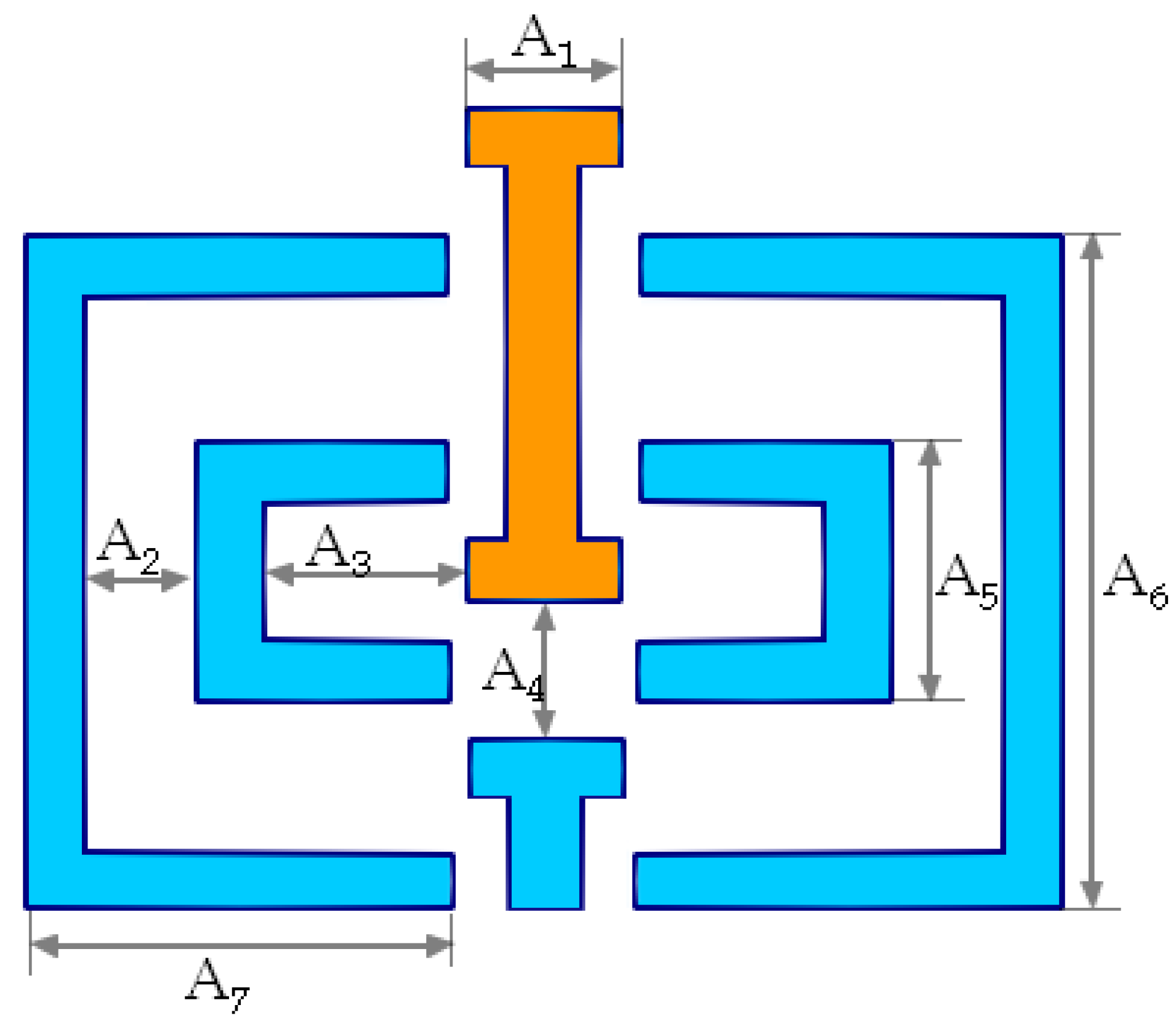
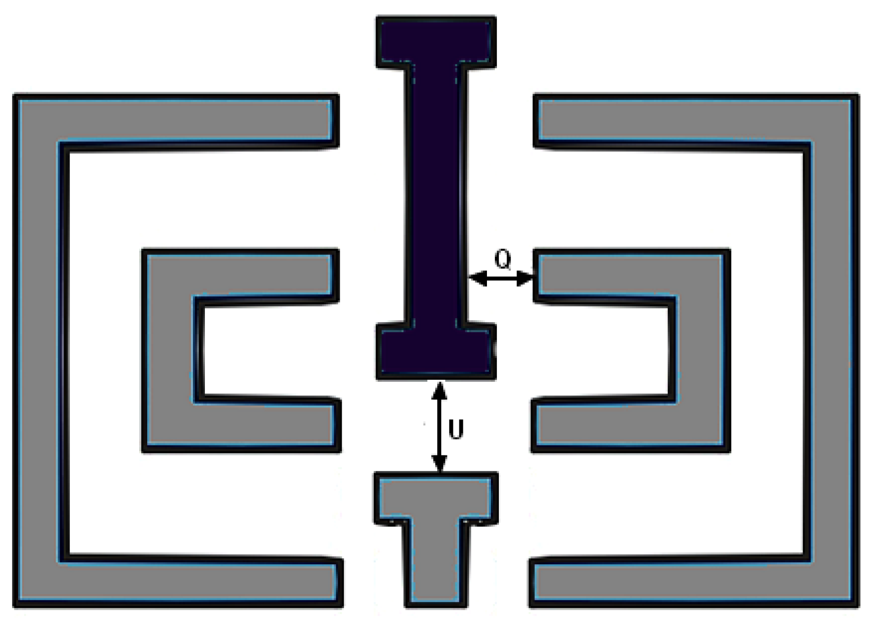
The modified geometry of the one proposed by Xu et al. [16] is used in this paper—a fixed element in the geometry was added to the eSRR to reduce the gap in the outer perimeter. This structure may have the effect of greater integration of the moving part in the unit cell with its immovable added part and may have an influence on the resonant frequencies. The proposed geometry is illustrated in Figure 1. Reconfiguration of eSRR could be done by using electrostatic force by using a MEMS-based comb driver [16]. This allows the desired modification of the resonant frequency, meaning that the control of the comb driver changes the arrangement of the conducting parts in the unit cell.

Figure 1.
Geometrical denotations of eSRR unit cell including widths, gaps, and lengths. The orange column is described as the movable I-shaped metal bar.
2.1. Design of the eSRR
The eSRR is designed on a 26 µm SiO2 layer and the overall size of eSRR unit cell is 100 × 100 µm. Material linewidth is 4 µm. The values of all parameters shown in Figure 1 are described in Table 1. Gap A4 is described as the point at which the tilt of the moving column is at its initial state. Width A1 describes the thickness of the end of the column. A3 is the distance between the eSRR and I-shaped movable column.

Table 1.
Dimensions included in Figure 1.
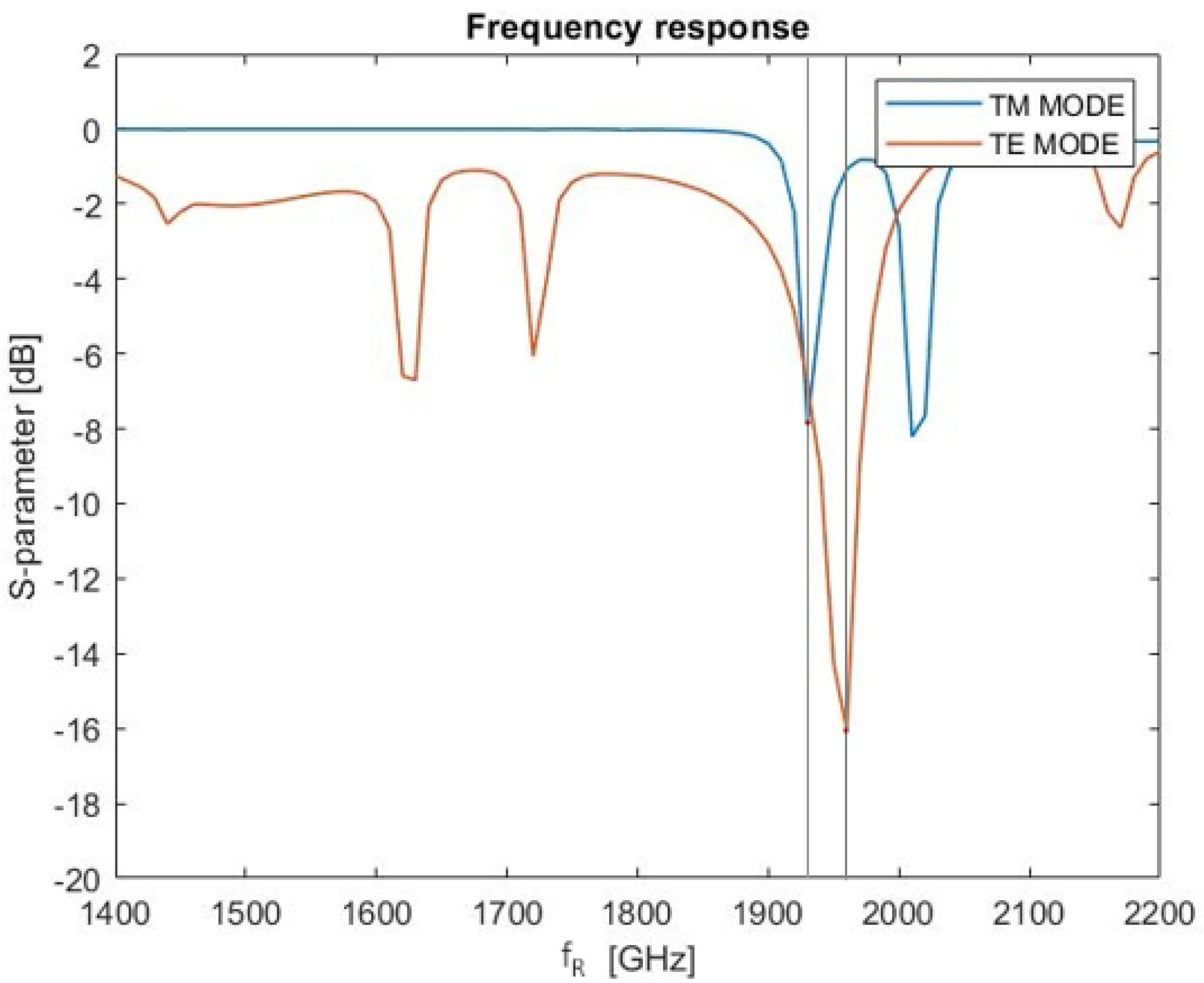
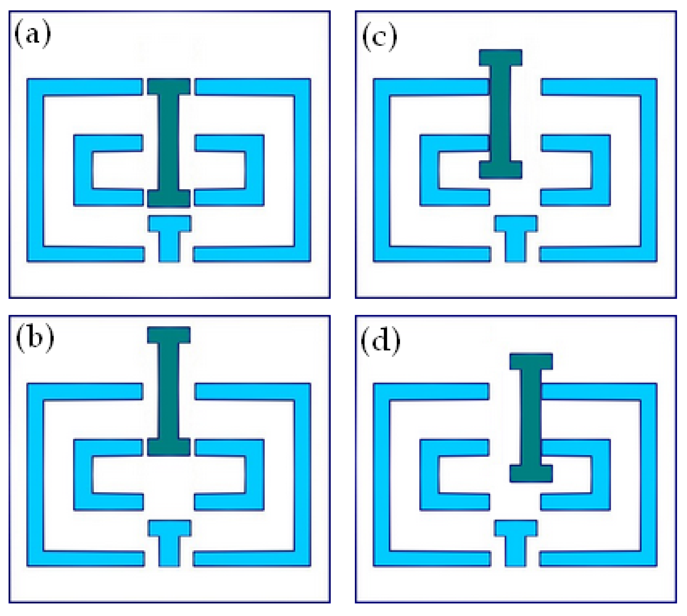
The middle I-shaped metal bar can be moved in vertical and horizontal directions. Figure 1 shows the initial point of the I-shaped metal bar, while the reflection coefficient S11 frequency response for this configuration is shown in Figure 2. At this point, the bar can be moved 6 µm to the right and 6 µm to the left with a step size of 2 µm. The maximum range is equal to 6 µm because at this point the moving column touches the stationary part of the unit cell. This is the only Y-axis height for which right and left sliding is assumed to be allowed. The movable column can also be moved up and down. Taking the position of the column shown in Figure 3a as a reference, its maximum upward displacement is 16 µm with a step equal to 2 µm in the upward Y-axis. The maximum deflection points in the X and Y axes are shown in Figure 3. MEMS technology constructed in this way (for such constraints) could allow even more precise control of the geometry of the unit cell, and thus the selection of parameters such as the resonant frequency with greater accuracy.
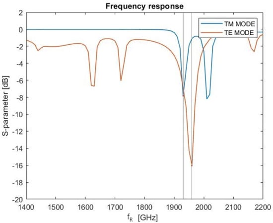
Figure 2.
S11 frequency response for TM and TE modes for geometry in its base configuration. Approximate values plotted for a larger sampling step equal to 0.01 THz.
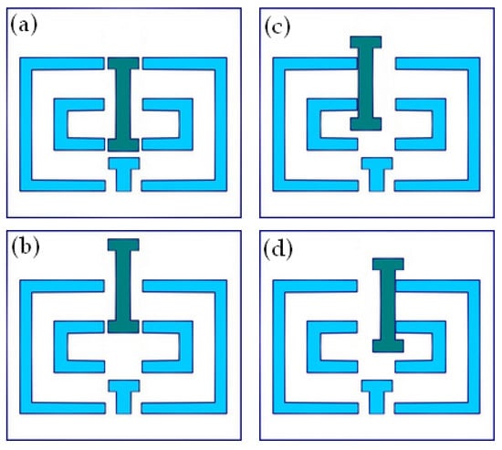
Figure 3.
The maximum deflection points of the movable I-shaped metal bar in the X and Y axes: (a) the initial state of the bar, where deflection is equal to zero; (b) maximum swing of the moving column, 16 µm; (c) maximum leftward deflection in the X-axis, equal to 6 µm; (d) maximum rightward deflection in the X-axis, equal to 6 µm.
2.2. Model and Additional Dielectric Layer
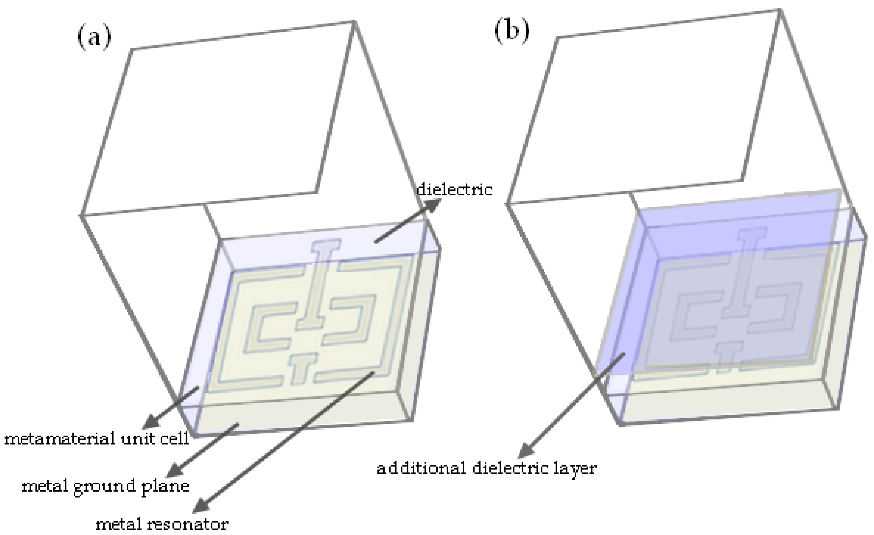
The proposed metamaterial unit cell consists of a metal ground plane, a metal resonator, and a dielectric layer. Au is proposed for the composition of the ground plane and metal resonator. For the component of the dielectric layer, SIO2 is proposed. Attaching the very thin layer of dielectric (material under test) to the metasurface will change the resonant frequency. In this paper, the influence of a several-microns-thin dielectric layer with various values of dielectric permittivity (εr = 1, 2, 3, 4, 5) is examined. The behavior of the frequency response and the change of the resonant frequency for specific arrangements of the I-shaped metal bar were investigated during simulations. The experiments were performed with terahertz (THz) radiation incident on the eSRR in TM (electric field component parallel to I-shaped metal bar) and TE (electric field component perpendicular to I-shaped metal bar) modes. A simplified structure of the proposed metasurface model is shown in Figure 4. Additional dielectric layer width is equal to 15 µm. The details of the numerical model are the same as in [17].

Figure 4.
Simplified (single element) structure of the metasurface model: (a) proposed metasurface structure; (b) proposed metasurface structure with very thin additional dielectric layer.
3. Results
Simulations were performed to find the change in resonant frequency as a function of offseting the I-shaped metallic bar. The verified data were then compared with data from the same study, only with the assumption that there is a thin dielectric layer in vicinity of the metasurface. The film thickness in the design was considered to be 15 µm, as most film solutions on the market assume a thickness from 6/7 µm upwards [18]. Reviewing the simulation results, many relationships can be seen. While studying the behavior of eSRR under various geometries, the behavior of resonant frequency was evaluated. With some eSRR geometries, more than one resonant frequency appeared in the considered frequency band. Given the goal of this study, the possibility of having an eSRR whose resonant frequency changes when the geometry changes was explored; additionally, more stable resonances were omitted whenever possible, with the focus being on the larger and visibly changing ones.
All simulations were performed in the COMSOL Multiphysics 5.4 environment. The creation of a numerical model suitable for subsequent simulations requires the completion of several necessary work steps. The first of these is the creation of the structure. This stage includes the following: Creating the cuboid in which the eSRR will be placed (Figure 4a). The dimensions used in the design to create the cuboid are 100 × 100 × 140 µm. A substrate layer must then be created, for the eSRR this will be a dielectric substrate on which the SRR geometry will be created from conductive elements. The dimensions of the substrate (Figure 4b) are 100 × 100 × 20 µm, respectively. The final step in the construction of the elementary cell structure is to apply the geometry of the conductive parts.
The second stage of the SRR model design is to assign physical properties to the individual elements. The conductive layers were given the physical parameters of gold, for which the electrical conductivity was determined as 4.09 × 10⁷ (S/m). The relative permittivity (εR) of the substrate is 3.9 and the void space (defined as air) in the solid is equal to 1.
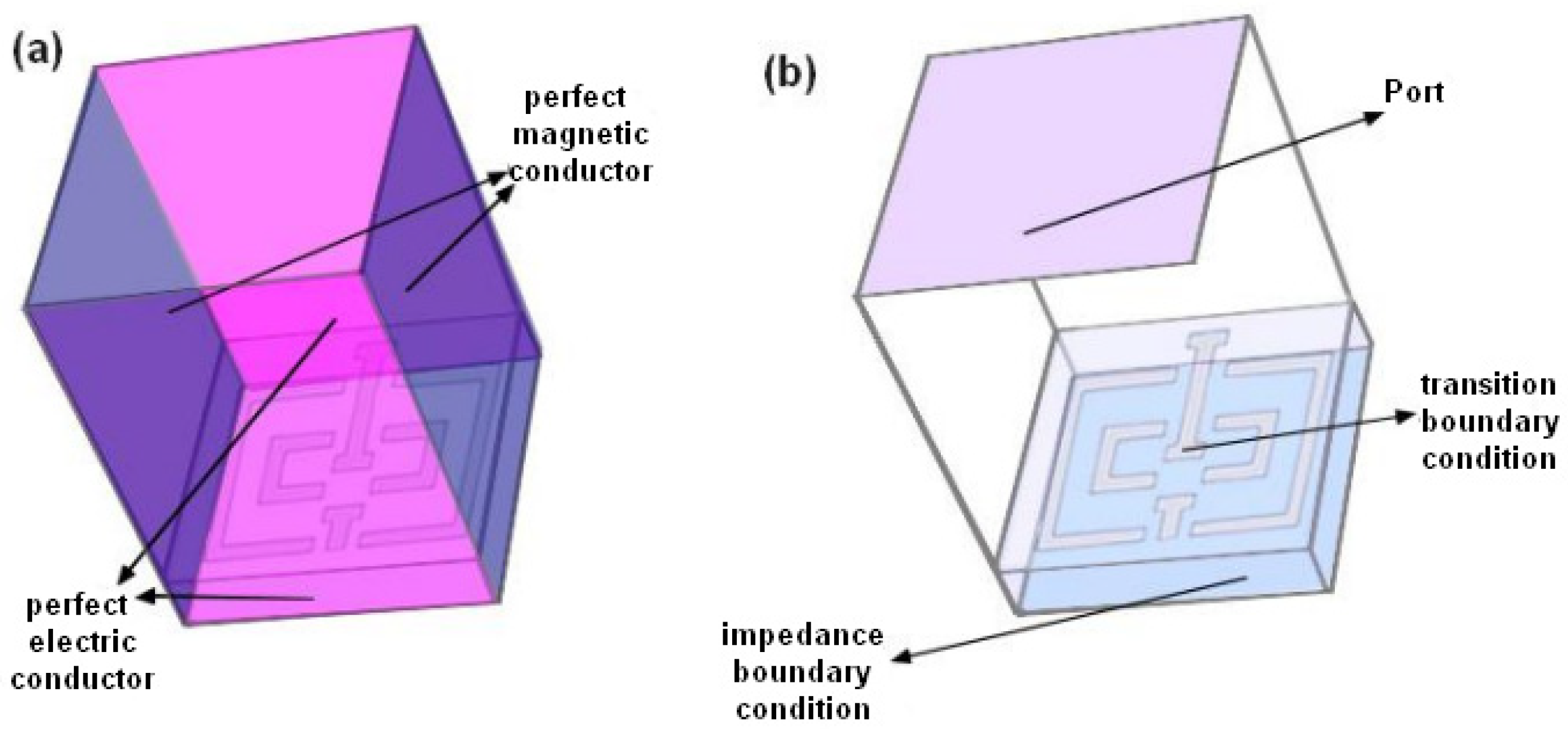
The third and final step in creating the numerical model is to define the boundary conditions. Thus, the following roles have been assigned to the planes present in the geometry: ports, perfect electrical conductors, perfect magnetic conductors, impedance and transition boundary conditions. Ports are used because electromagnetic energy is supplied and received into the model. The port allows and supports the calculation of the scattering parameter, but can also be used to excite the model. The boundary condition of an ideal electric conductor is a special case of the electric field boundary condition, which sets the tangential component of the electric field to zero. The boundary condition of an ideal magnetic conductor, on the other hand, is a special case of the boundary condition of the of the surface current, which sets the tangential component of the magnetic field, and therefore the and the surface current density to zero. The impedance boundary condition is useful at boundaries where the electromagnetic field penetrates only a short distance beyond the boundary. In contrast, the transient boundary condition is based on the assumption, that the wave propagates in the normal direction in a thin film. It represents a discontinuity in the tangential electric field. The position of the boundary conditions described above in the model is shown in Figure 5. For the model prepared in this way, a computational mesh was generated and then computations were performed using a direct solver. An FEM (Finite Element Method)-type analysis was performed to check the electromagnetic field distribution. The COMSOL Multiphysics 5.4 environment, by means of the computational operations described above, allows the target characteristics to be easily determined. The simulation results are determined for frequencies close to the resonance frequencies of the MM for the corresponding arrangements of the moving element in the given mode.

Figure 5.
Figure showing the planes of: (a) perfect electric conductor, perfect magnetic conductor; (b) port, impedance boundary condition, transition boundary condition.
3.1. Analysis for Scenario without a Dielectric Layer
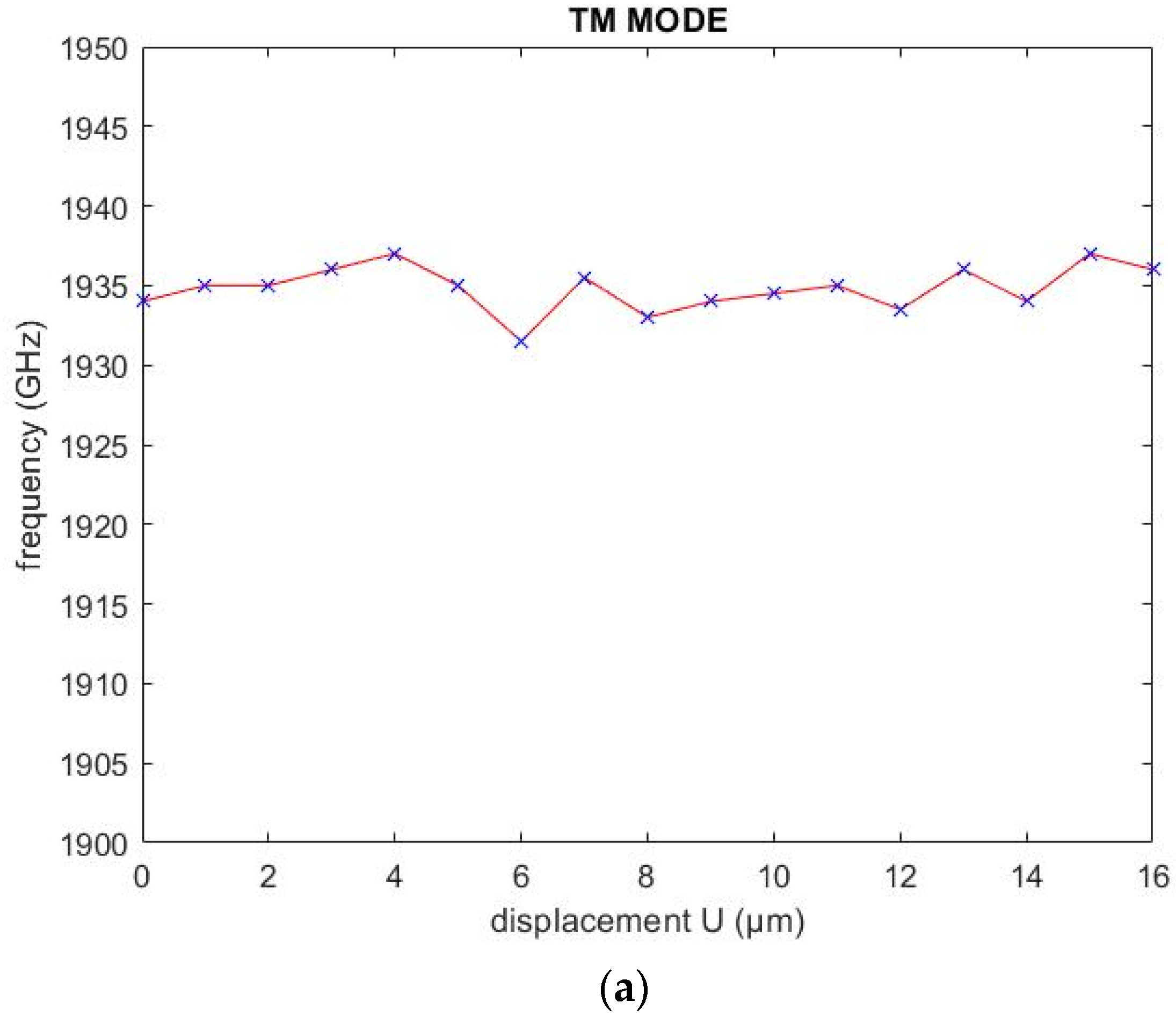
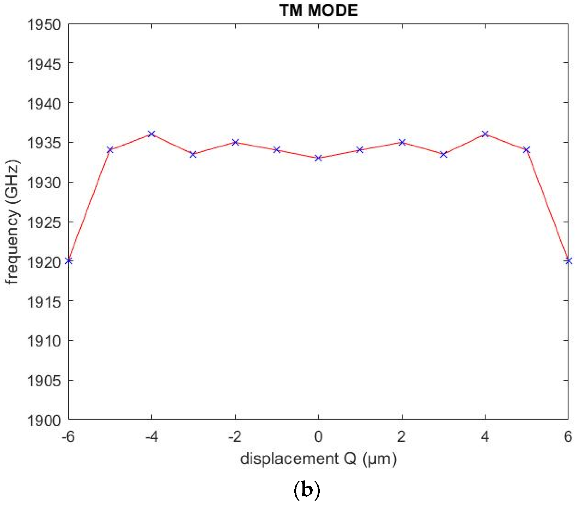
In Figure 6 the bias markings of the center column in different directions can be seen. In order to investigate the effect of electromagnetic coupling for eSRR in detail, the electromagnetic characteristics of the eSRR device with different values of U for zero bias Q are discussed. The effect of electromagnetic coupling was examined in the TE and TM modes. At Q = 0 µm and U = 0 µm, in TM mode the resonant frequency is 1.934 THz, as shown in Figure 7a. When changing the value of U to 2 µm there is increase of this frequency to 1.935 THz. At U = 6 µm there is the lowest resonant frequency equal to 1.931.5 THz. Then, by increasing the shift to U = 7 µm, the resonant frequency has value 1.935.5 THz. After that there is a small increase at U = 8 µm to 1.933 THz. Increasing the U value to 11 µm shows increasing resonance frequency value to 1.935 THz and then there are only two bigger increases, at U = 13 µm with frequency 1.936 THz and U = 15 µm with frequency equal to 1.937 THz. In this mode, the stability of the resonant frequency to the change in column offset can be seen, compared to other figures. At Q = 0 µm and U = 8 µm, the resonant frequency is 1.933 THz. By shifting the I-shaped metal bar to the left and thus manipulating the Q value by 2 µm, it can be observed, as in Figure 7b, that there is a small change of the resonant frequency with value equal to 1.935 THz. At the value of Q = 5 µm and Q = −5 µm, the resonance frequency starts to decrease, and at the point of contact between the moving column and the rest of the eSRR, i.e., for Q = −6 µm and Q = 6 µm, the resonance frequency drops to 1.92 THz. Frequency has fallen by as much as 0.014 THz.
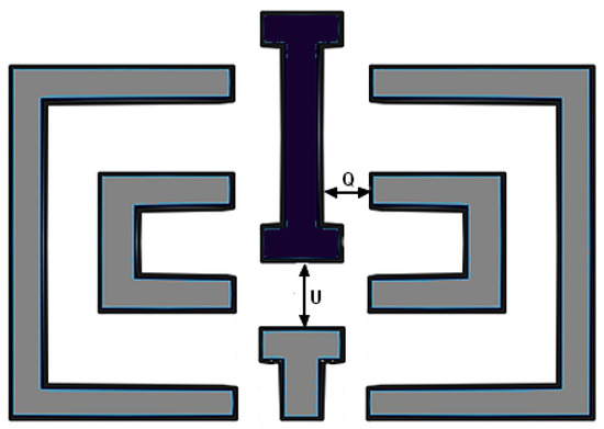
Figure 6.
Position of the central column at maximum tilt U = 8 µm and position of Q at zero tilt.
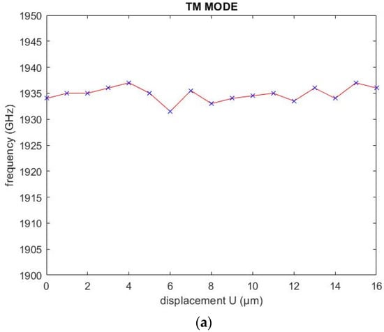
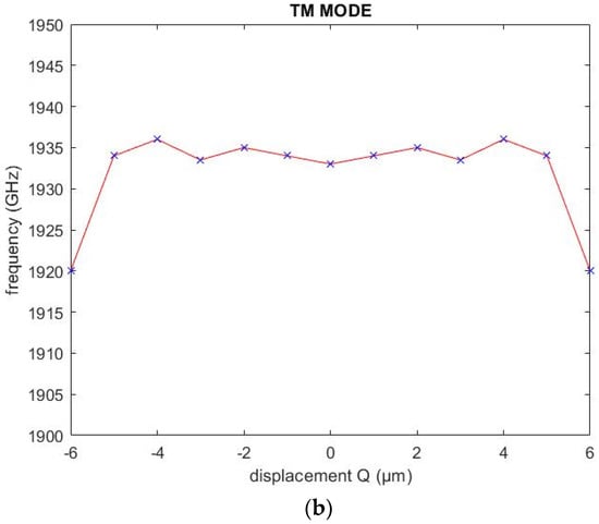
Figure 7.
Resonance values while changing the I-shaped position in TM mode: (a) change in resonance frequency when moving the center I-column metal bar up in 2 µm increments to a maximum excursion of 16 µm; (b) change in resonance frequency when moving the center column right and left in 2 µm up to a maximum excursion of 6 µm for a rightward shift and −6 µm for a leftward shift. Shifting in this direction is done for a value of U equal to 8 µm, i.e., at the center position of the moving I-shaped column.
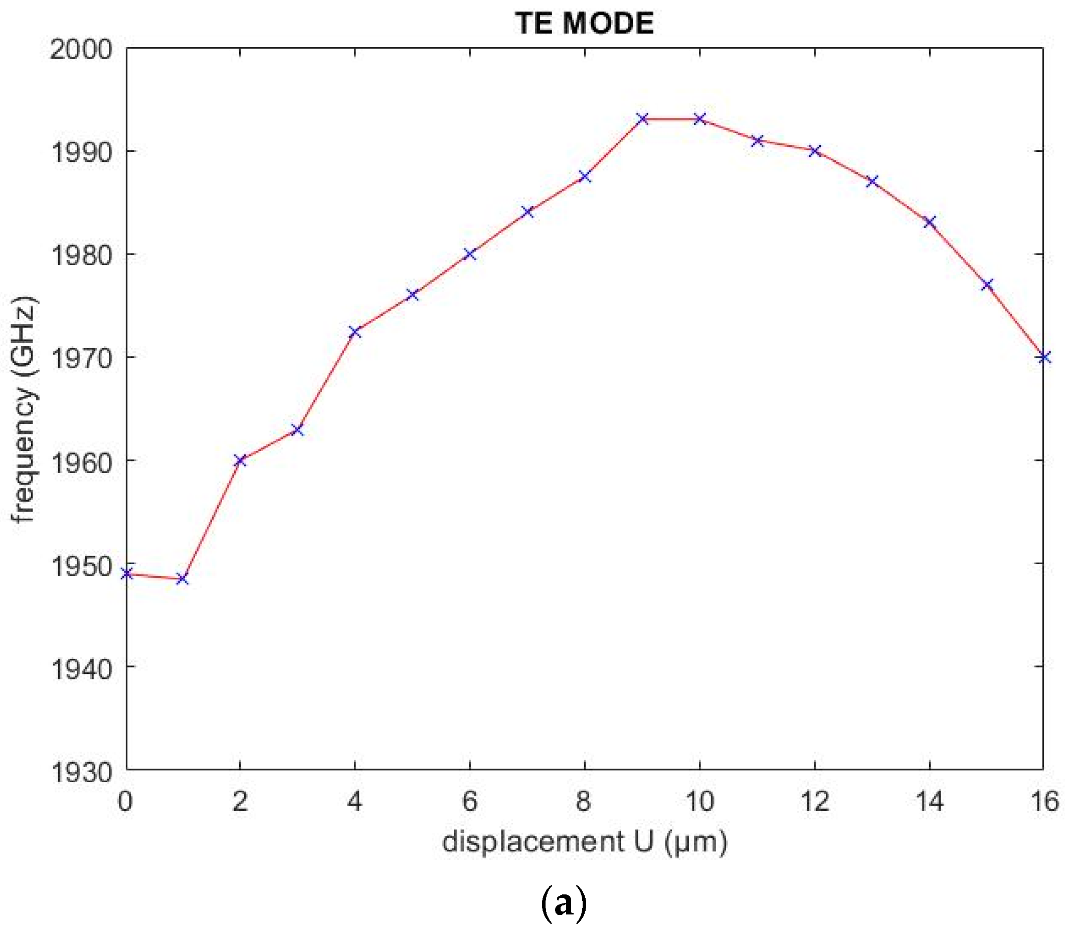
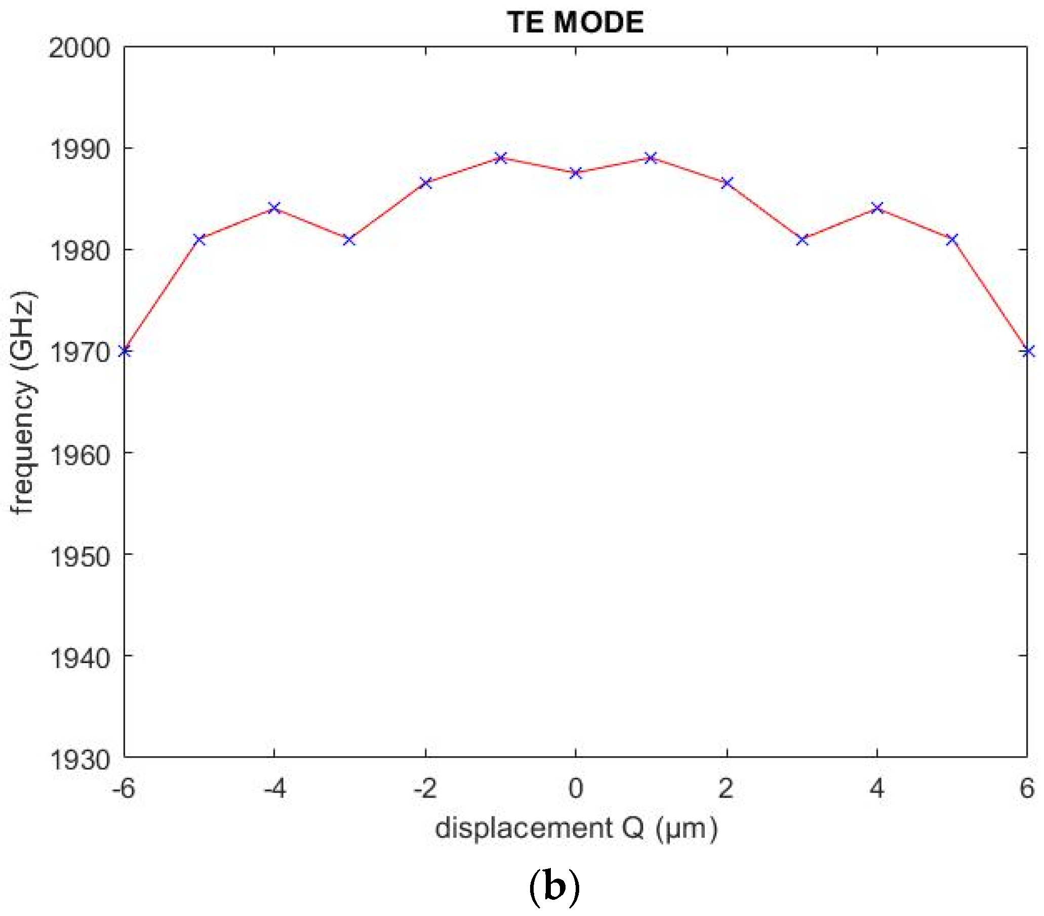
Finding the value of the resonant frequency depending on the change in position of the I-shaped metal bar is more complicated in the TE mode than in the TM mode. Although in TM mode two or even three resonances appeared with most geometry alignments and were sensitive to geometry change, in TE mode with some geometries there were multiple resonances that began to overlap. The readings of the main resonant frequency that appeared with each eSRR geometry was more complicated, which is not to say that this resonance maintained its stability longer than with TM mode. In the results shown in Figure 8 the resonances dependent on the change of position were included and those that showed their presence at each Q and U value. In Figure 8, the change in resonant frequency with tunable eSRR geometry in TE mode is shown.
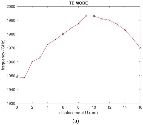
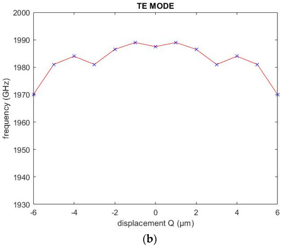
Figure 8.
Resonance frequency values while changing the I-shaped position in TE mode: (a) change in resonance frequency value when moving the center I-column metal bar up in 2 µm increments to a maximum excursion of 16 µm; (b) change in resonance frequency value when moving the center column right and left in 2 µm up to a maximum excursion of 6 µm for a rightward shift and −6 µm for a leftward shift. Shifting in this direction is done for a value of U equal to 8 µm, i.e., at the center position of the moving I-shaped column.
As can be seen in Figure 8a, the resonant frequency for Q = 0 µm and U = 0µm was 1.949 THz. The resonant frequency, when shifted to a height of 2 µm, has increased to 1.96 THz. In this mode, the sensitivity of the resonant frequency to a change in the geometry of the unit cell can be seen. By changing the geometry, the resonant frequency increased to 1.993 THz at Q = 0 µm and U = 9 µm, U= 10 µm. By increasing the position to Q = 0 µm and U = 12 µm, resonant frequency began to fall to the value of 1.99 THz. The decrease in resonant frequency has continued and in the position of Q = 0 µm and U = 16 µm reached 1.97 THz. Figure 8 only contains the values of one resonance, which appeared before shifting, at the zero position of the geometry. There are more than one, two, or even three resonances in the TE mode. When moving the I-shaped metallic bar, over a height of 10, four resonances started to build up, which even had a similar amplitude. This density of resonances causes them to overlap, which makes it difficult to recognize the shift. In Figure 8b it can be seen that the resonant frequency for Q = 0 µm, and U = 8µm is 1.987.5 THz. It increases at Q = 1 µm and Q = −1 µm with frequency equal to 1.989 THz. Then the frequency fell to 1.981 THz with Q = −3 µm and Q = 3 µm. Moving toward the maximum position, the resonant frequency drops to 1.97 THz but has a small increase at Q = 4 µm and Q = −4 µm with frequency equal to 1.984 THz.
3.2. Analysis for Scenario with a Dielectric Layer
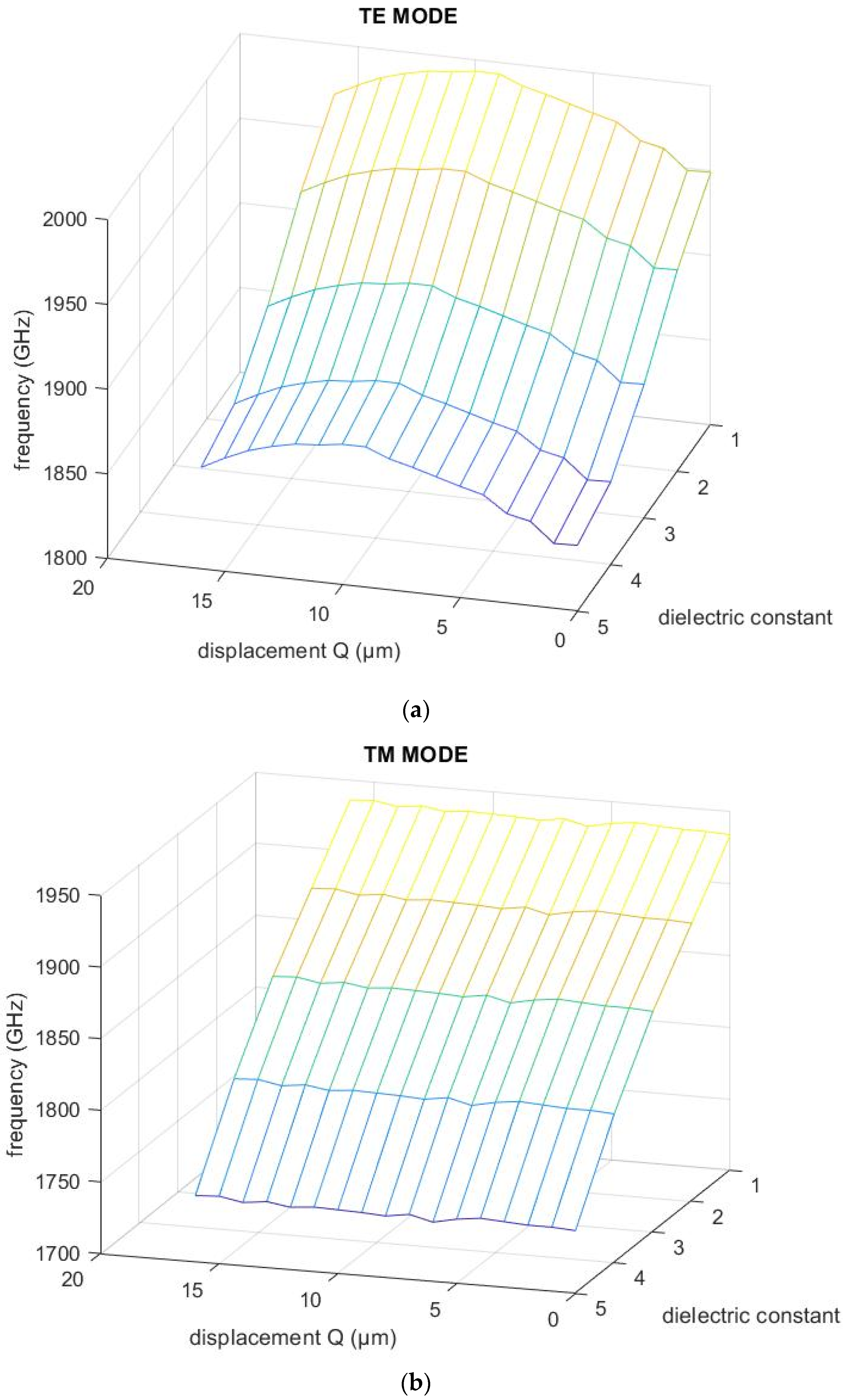
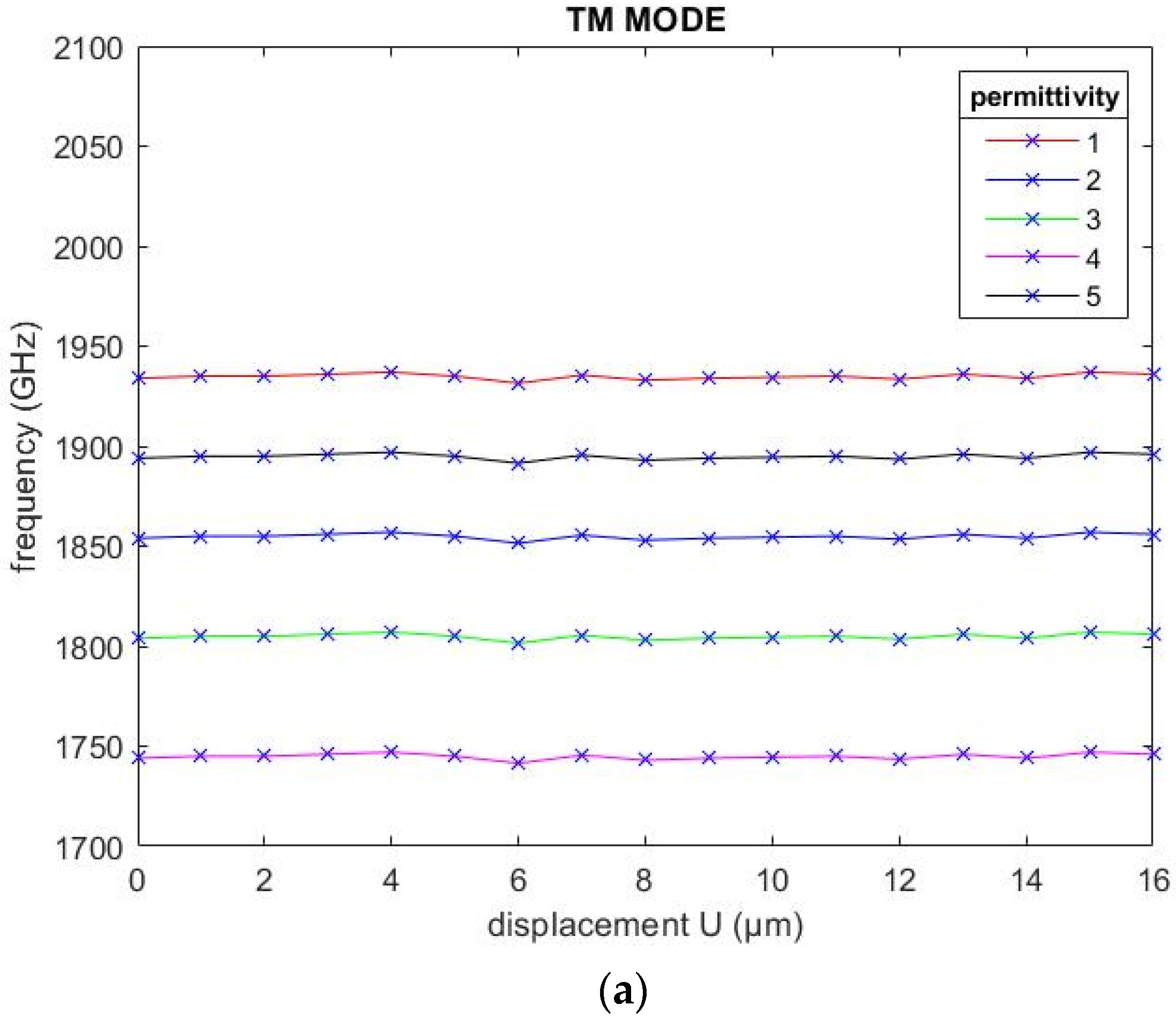
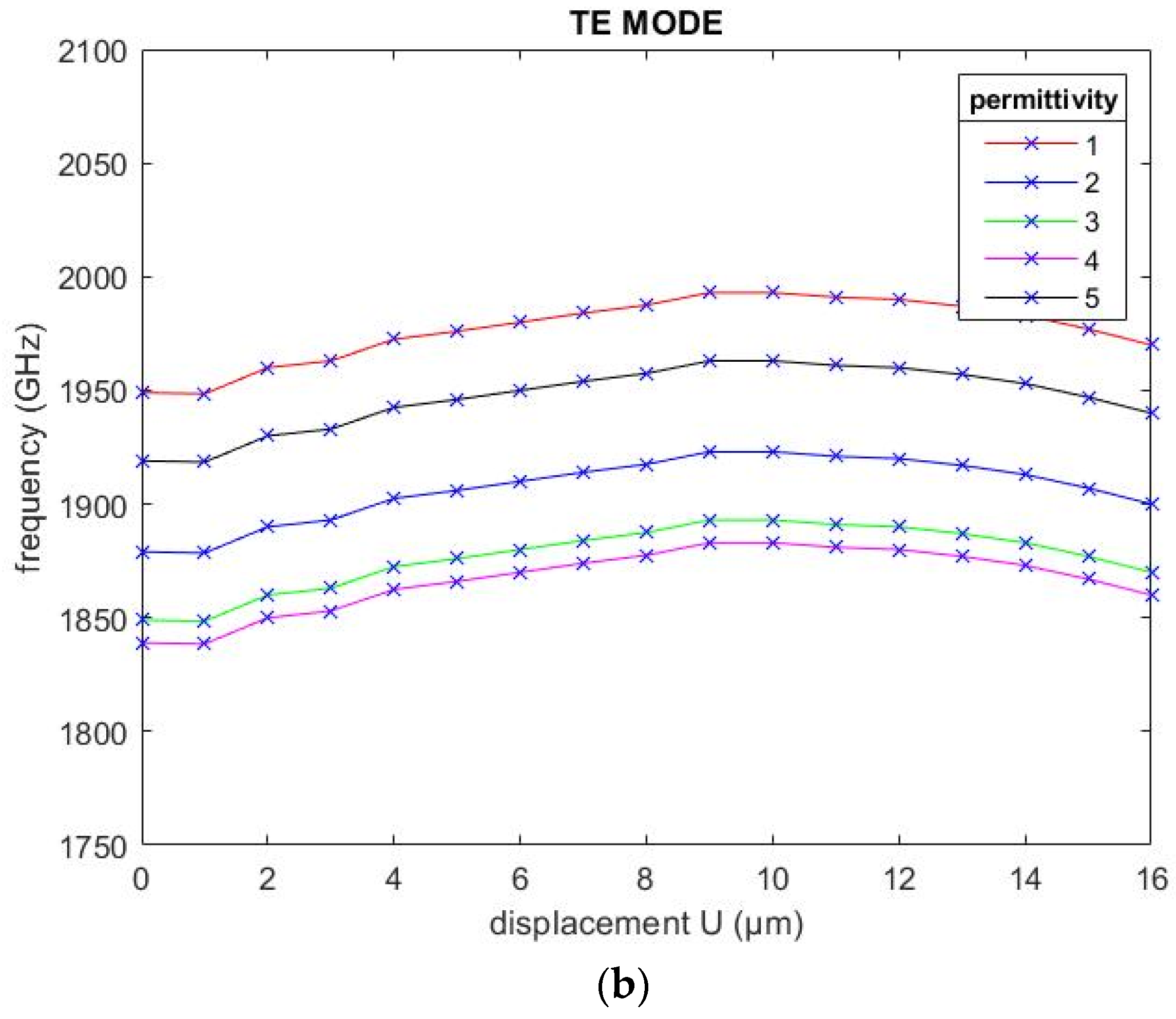
Finally, an analysis of tunable metasurface sensor interaction with an additional thin dielectric layer was performed. The goal was to find the changes of tunability characteristics (as shown in Figure 8a) caused by changes of thin layer dielectric properties (because of inhomogeneities or thickness variations). The layer has been designed and placed 15 µm above the metasurface. Such a situation is possible if the measuring head of the THz spectroscope is fixed with an MS sensor (which is in the focal point of the terahertz Gaussian beam) and the examined dielectric foil is in vicinity of the sensor. The behavior of the model has been studied for different values of dielectric permittivity of the thin layer. Simulations were performed for permittivity values from 1 to 5. Shifts in resonance frequencies are shown in Figure 9. By manipulating the value of the permittivity coefficient, both the amplitude and frequency of the selected resonances is changed significantly.
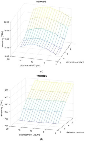
Figure 9.
Resonance change as a function of permittivity value of an additional layer: (a) change in resonant frequency in TE mode; (b) change in resonant frequency in TM mode.
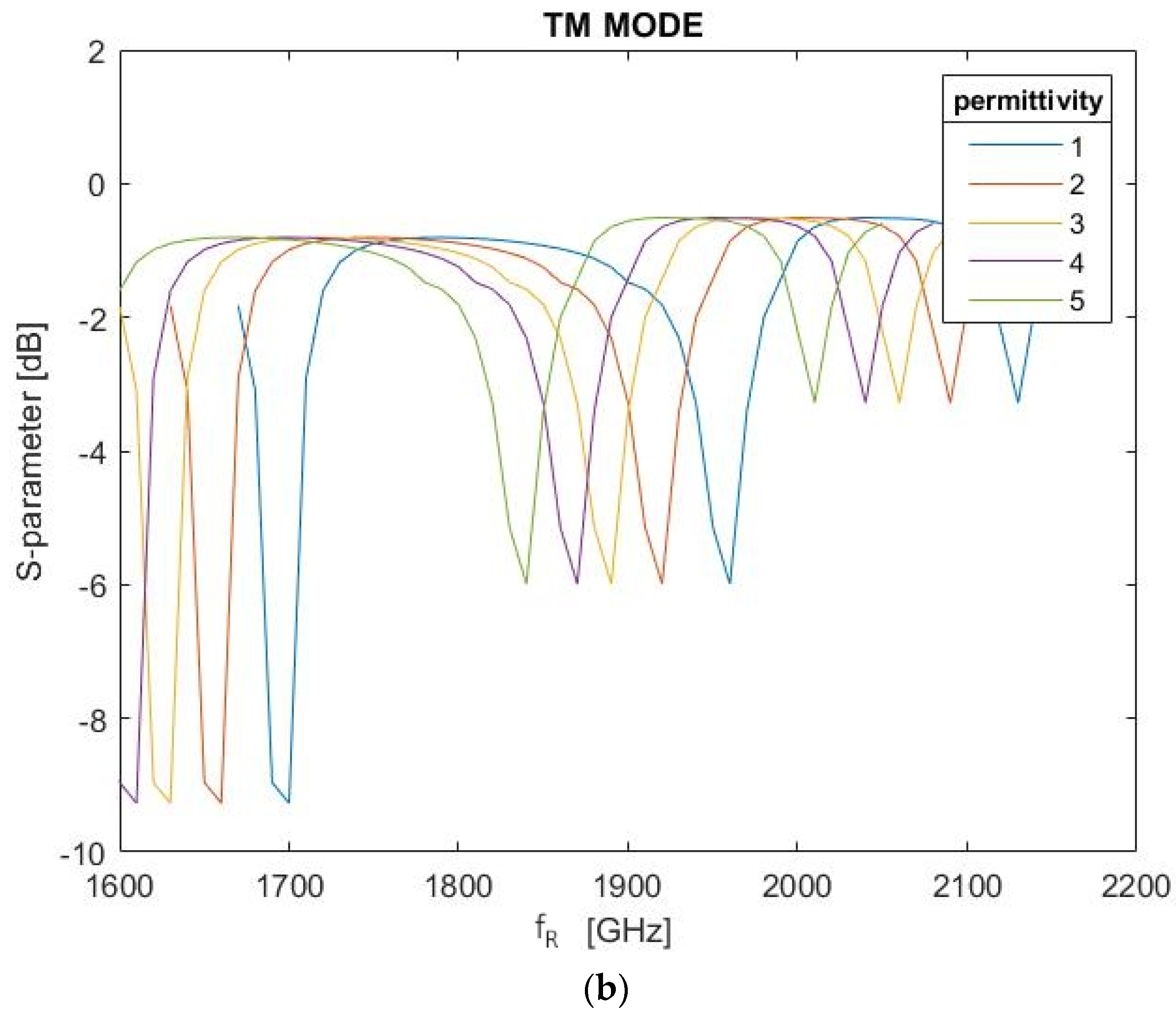
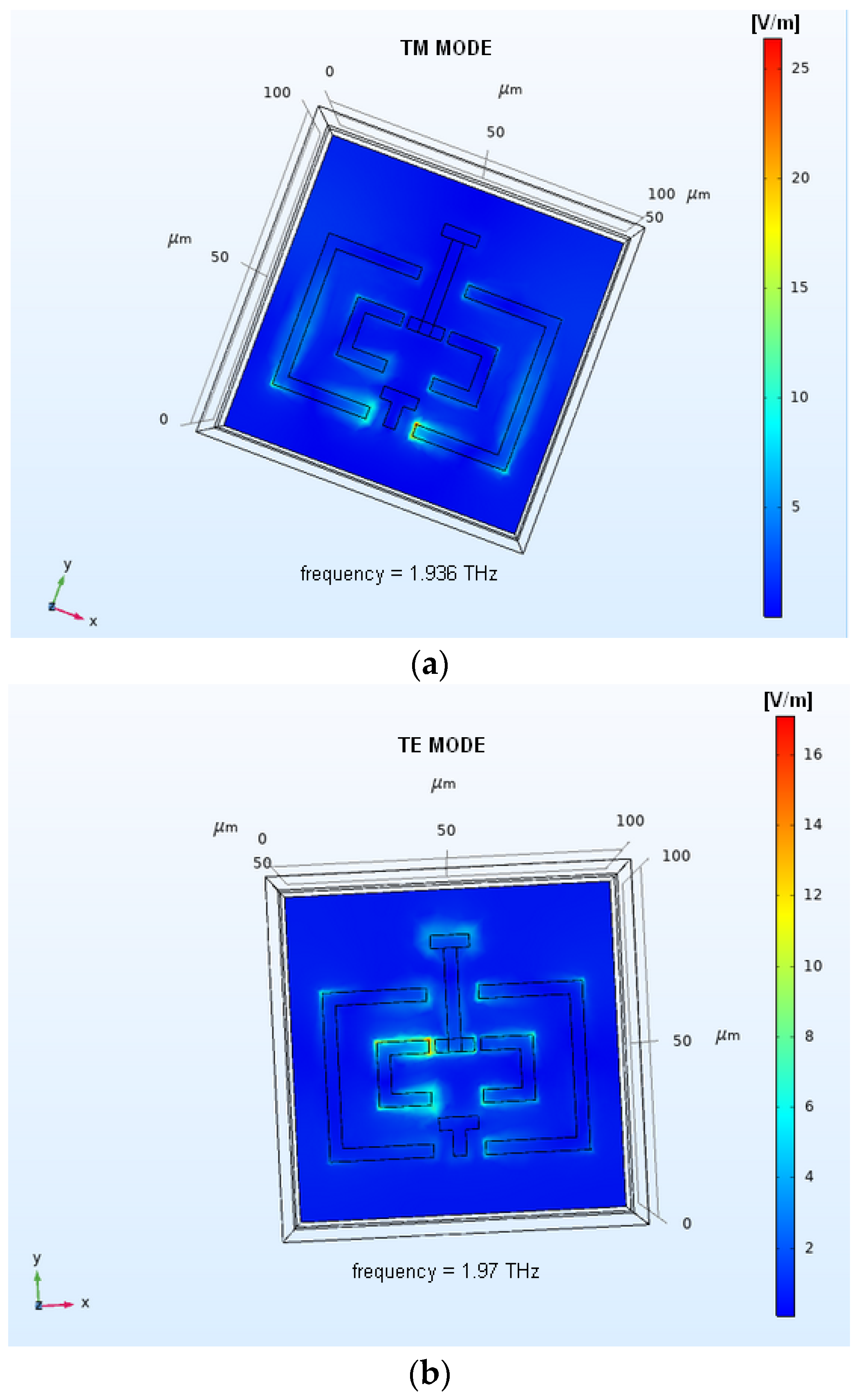
As can be seen in Figure 9 in the TE and TM modes, increasing the value of the permittivity caused a decrease in the resonant frequency fR. The resonant frequency in the TM mode responded with less sensitivity to I-shaped metal bar shifts. Figure 10 shows reflection coefficient S11 frequency response changes caused by various permittivities of an additional layer in case of a fixed arrangement of the eSRR geometry, i.e., Q = 0 µm and U = 8 µm. As can be seen in Figure 10a, there are several resonances, although they respond with the same shift to the dielectric layer. The influence of additional layer permittivity change on resonant frequencies is more efficient than metasurface tenability range. The plots of Figure 10 show exactly how large the jumps between the resonance frequencies are for various layer properties. A dielectric layer 15 µm thick with a permittivity coefficient equal to two resulted, as seen in Figure 11b, leading to a shift in the reduction of the resonant frequency by 30 GHz in the TE mode. Increasing the coefficient to three results in a decrease by another 40 GHz. Finally, from the initial value at a factor of five, the resonant frequency decreases by 110 GHz. In the TM mode, as seen in Figure 11a, applying a layer with a permittivity coefficient of two to the unit cell resulted in a shift, reducing the resonant frequency by 40 GHz. Increasing the coefficient to three results in a decrease of another 40 GHz. Finally, from the initial value with a coefficient equal to five, the resonant frequency decreases by 190 GHz. The electric field norm for TE and TM modes are shown in Figure 12. Such a figure shows the differences in the distribution of the electric field in different modes.
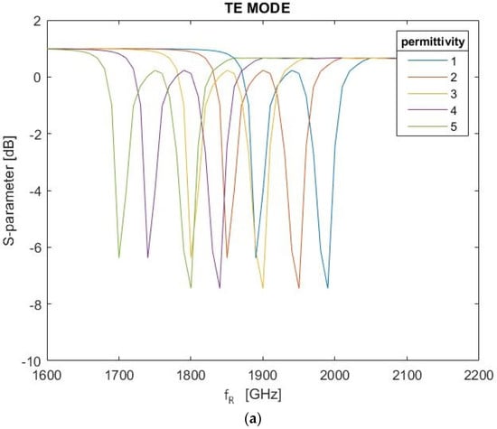
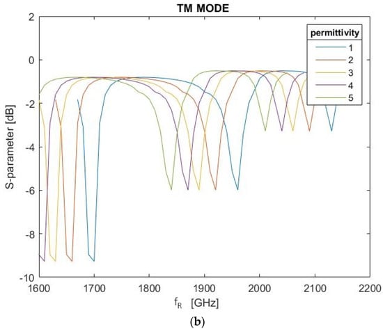
Figure 10.
S11 frequency response change caused by various permittivities of an additional layer for geometry Q = 0 µm and U = 8 µm with larger sample step equal to 0.01 THz: (a) TE mode, (b) TM mode.
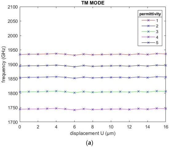
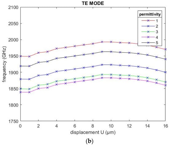
Figure 11.
Resonant frequency change as a function of permittivity of an additional layer—2D plot in case of: (a) TM mode, (b) TE mode.
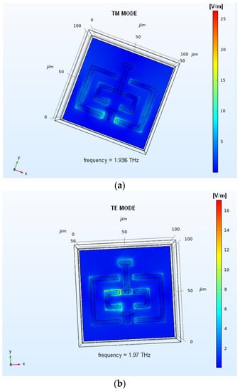
Figure 12.
Examples for electric field norm with shift of tunable bar at position U = 16 µm and Q = 0 µm: (a) TM mode, (b) TE mode.
The distributions of resonant frequency as a function of displacement U and dielectric layer relative permittivity εr − fR(U, εr) were approximated using simple polynomial expressions, as follows:
where: fRTE and fRTM are resonant frequencies (in GHz) in the case of the TE and TM modes, respectively. This enables the simple calculation of the permittivity based on the following formulas:
One can observe that the sensitivity of permittivity calculation is higher in the case of the TE mode. When examining the thin dielectric layer, any change in the measured relative permittivity can be associated with various kinds of material inhomogeneities or variations of dimensions. A detailed analysis of this aspect will be the object of further research.
4. Conclusions
The use of MEMS technology in metasurfaces allows for subtle changes in the resonant frequency value specified for each eSRR geometry. Such behavior can be utilized to extend the possibilities of the evaluation of thin dielectric layers. It is possible to observe not just the change of one resonant frequency caused by change of dielectric parameters of MUT, but it is possible to observe this effect for many resonant frequencies (from tenability range of the metasurface sensor). This could be more beneficial in case of strongly dispersive materials. The resonant frequency is not sensitive to all changes in the geometry of the unit cell, but the analyzed metasurface responds very sensitively to a change in the relative permittivity coefficient. The parallel application of two methods (MEMS technology and additional dielectric layer) allows for the more sensitive control of resonant frequency. This is a very desirable feature because the methods can be combined with each other as needed. Furthermore, approximation-based formulas were derived that enable the simple evaluation of MUT permittivity and, in consequence, permittivity-related inhomogeneities.
In further work, other types of structural elements will be designed and validated in order to increase the tunability range of the metasurface resonator, and more analysis will be performed in order to evaluate sensitivity for various kinds of inhomogeneities and for variations of measuring conditions, such as the distance of the MS sensor and material under test.
Author Contributions
Conceptualization, P.L.; methodology, P.L. and P.G.; simulations, P.G.; validation, P.L.; investigation, P.G.; writing—original draft preparation, P.G.; writing—review and editing, P.L.; supervision, P.L.; project administration, P.L.; funding acquisition, P.L. All authors have read and agreed to the published version of the manuscript.
Funding
This work was done within the project co-financed by the Polish National Agency for Academic Exchange (NAWA, Poland) and German Academic Exchange Service (DAAD, Germany), under the grant no. PPN/BDE/2021/1/00012/U/00001. The APC was funded by the Research Fund of the Faculty of Electrical Engineering (West Pomeranian University of Technology, Szczecin, Poland).
Institutional Review Board Statement
Not applicable.
Informed Consent Statement
Not applicable.
Conflicts of Interest
The authors declare no conflict of interest.
References
- Grimberg, R. Electromagnetic metamaterials. Mater. Sci. Eng. B 2013, 178, 1285–1295. [Google Scholar] [CrossRef]
- Chang, Y.; Wei, J.; Lee, C. Metamaterials–from fundamentals and mems tuning mechanisms to applications. Nanophotonics 2020, 9, 3049–3070. [Google Scholar]
- Shadrivov, I.V.; Morrison, S.K.; Kivshar, Y.S. Tunable split-ring resonators for nonlinear negative-index metamaterials. Opt. Express 2006, 14, 9344–9349. [Google Scholar] [CrossRef] [PubMed]
- Kumar, R.; Kumar, M.; Chohan, J.S.; Kumar, S. Overview on metamaterial: History, types and applications. Mater. Today Proc. 2022, 56, 3016–3024. [Google Scholar] [CrossRef]
- Turpin, J.P.; Bossard, J.A.; Morgan, K.L.; Werner, D.H.; Werner, P.L. Reconfigurable and tunable metamaterials: A review of the theory and applications. Int. J. Antennas Propag. 2014, 2014, 429837. [Google Scholar] [CrossRef]
- Bang, S.; Kim, J.; Yoon, G.; Tanaka, T.; Rho, J. Recent advances in tunable and reconfigurable metamaterials. Micromachines 2018, 9, 560. [Google Scholar] [CrossRef] [PubMed]
- Zhu, W.M.; Liu, A.Q.; Zhang, X.M.; Tsai, D.P.; Bourouina, T.; Teng, J.H.; Zhang, X.H.; Guo, H.C.; Tanoto, H.; Mei, T.; et al. Switchable magnetic metamaterials using micromachining processes. Adv. Mater. 2011, 23, 1792–1796. [Google Scholar] [CrossRef] [PubMed]
- Fu, Y.H.; Liu, A.Q.; Zhu, W.M.; Zhang, X.M.; Tsai, D.P.; Zhang, J.B.; Mei, T.; Tao, J.F.; Guo, H.C.; Zhang, X.H.; et al. A micromachined reconfigurable metamaterial via reconfiguration of asymmetric split-ring resonators. Adv. Funct. Mater. 2011, 21, 3589–3594. [Google Scholar] [CrossRef]
- Liu, M.; Susli, M.; Silva, D.; Putrino, G.; Kala, H.; Fan, S.; Cole, M.; Faraone, L.; Wallace, V.P.; Padilla, W.J.; et al. Ultrathin tunable terahertz absorber based on mems-driven metamaterial. Microsyst. Nanoeng. 2017, 3, 17033. [Google Scholar] [CrossRef]
- Han, Z.; Kohno, K.; Fujita, H.; Hirakawa, K.; Toshiyoshi, H. Mems reconfigurable metamaterial for terahertz switchable filter and modulator. Opt. Express 2014, 22, 21326–21339. [Google Scholar] [CrossRef] [PubMed]
- Xu, R.-J.; Lin, Y.-S. Actively mems-based tunable metamaterials for advanced and emerging applications. Electronics 2022, 11, 243. [Google Scholar] [CrossRef]
- Xu, J.; Yang, R.; Fan, Y.; Fu, Q.; Zhang, F. A review of tunable electromagnetic metamaterials with anisotropic liquid crystals. Front. Phys. 2021, 9, 633104. [Google Scholar] [CrossRef]
- Pitchappa, P.; Manjappa, M.; Ho, C.P.; Singh, R.; Singh, N.; Lee, C. Active control of electromagnetically induced transparency analog in terahertz mems metamaterial. Adv. Opt. Mater. 2016, 4, 541–547. [Google Scholar] [CrossRef]
- Liang, Y.; Koshelev, K.; Zhang, F.; Lin, H.; Lin, S.; Wu, J.; Jia, B.; Kivshar, Y. Bound states in the continuum in anisotropic plasmonic metasurfaces. Nano Lett. 2020, 20, 6351–6356. [Google Scholar] [CrossRef] [PubMed]
- Pang, K.; Alam, M.Z.; Zhou, Y.; Liu, C.; Reshef, O.; Manukyan, K.; Voegtle, M.; Pennathur, A.; Tseng, C.; Su, X.; et al. Adiabatic frequency conversion using a time-varying epsilon-near-zero metasurface. Nano Lett. 2021, 21, 5907–5913. [Google Scholar] [CrossRef] [PubMed]
- Xu, T.; Xu, R.; Lin, Y.-S. Tunable terahertz metamaterial using electrostatically electric split-ring resonator. Results Phys. 2020, 19, 103638. [Google Scholar] [CrossRef]
- Lopato, P.; Herbko, M. Evaluation of selected metasurfaces’ sensitivity to planar geometry distortions. Appl. Sci. 2019, 10, 261. [Google Scholar] [CrossRef] [Green Version]
- HINDALCO, Aluminium Foil Applications. Available online: https://www.hindalco.com/ (accessed on 22 June 2022).
Publisher’s Note: MDPI stays neutral with regard to jurisdictional claims in published maps and institutional affiliations. |
© 2022 by the authors. Licensee MDPI, Basel, Switzerland. This article is an open access article distributed under the terms and conditions of the Creative Commons Attribution (CC BY) license (https://creativecommons.org/licenses/by/4.0/).

