Article

Electro-Optic Sensor for Measuring Electrostatic Fields in the Frequency Domain

1
European Organization for Nuclear Research (CERN), 1211 Geneva, Switzerland
2
Department of Computer Science, School of Computing and Engineering, University of Huddersfield, Huddersfield HD1 3DH, UK
*
Author to whom correspondence should be addressed.
Appl. Sci. 2022, 12(17), 8544; https://doi.org/10.3390/app12178544
Submission received: 25 July 2022 / Revised: 17 August 2022 / Accepted: 25 August 2022 / Published: 26 August 2022
(This article belongs to the Special Issue Advances in Electro-Optical Engineering)

Abstract

:
Precise measurements of electrostatic fields in harsh environments are required in fields ranging from particle accelerators to industrial installations. Many techniques disrupt the field distribution due to the presence of conductors. We present a fully dielectric sensor for very harsh environmental conditions, that exploits the Pockels effect manifested by electro-optic crystals. This system is designed to allow DC measurements to be performed in the frequency domain. The paper discusses an analytical model and simulations of the system, validated with experimental results. The working principle of the measurement technique is explained in detail along the known limitations and possible solutions to further increase the performance.

1. Introduction

Electro-Optic (EO) crystals are increasingly used for measurements of electromagnetic fields [1], as they enable an incident electric field to be converted into a modulation of an optical beam. When exposed to an electric field, the refractive index of an EO crystal changes, which retards the phase of the traversing optical beam. If the phase retardation is linearly proportional to the incident field’s magnitude, this phenomenon is described as the Pockels effect [2]. Since the field intensity is effectively encoded onto the laser beam, it can be recovered using different optical configurations and approaches [3].
EO crystals can be used for operation in harsh environments such as particle accelerators and the speed at which the Pockels effect occurs makes EO crystals suited to high-frequency applications [4,5,6]. Because of these reasons several EO beam diagnostic tools have been developed, mostly regarding bunch length monitoring exploiting different EO techniques [7,8,9]. Some relevant experiments have been also carried out on high frequency Beam Position Monitors(BPMs) [10] for measuring the transverse position variation within a bunch of a particle beam [11,12].
Conversely, a DC or quasi-DC electromagnetic field causes movement of free charge carriers to the edges of the crystal creating a space charge region which in turns produces an internal electric field. This phenomenon changes the crystal’s properties and its response to external electric fields, affecting the accuracy of the measurement. Previous applications limited the use of EO crystals to measurements above 20 Hz [13], unless the effect of space charge was analytically compensated [14] or avoided using a rotary stage [15].
Other techniques, not based on EO materials, for electrostatic field measurements are reported in the literature, e.g., induction probes, oscillating parallel plate sensors and field mills [16]. However, they all disturb the measured electric field due to the presence of conductors. Furthermore, some ordinarily used sensors, like induction probes, need frequent re-zeroing, rendering measurements over a long time not possible.
We present an electrostatic field sensor composed of two EO crystals: one coupling to the measured electric field and a second one introducing an intentional modulation with a biasing electric field. The bias field sets the working point of the system, and can be used to compensate for errors caused by space charge, temperature drift, laser fluctuations and other similar phenomena.
Additionally, modulation of the bias field makes it possible to measure a DC field in the frequency domain. This novel approach for compensating the space charge extends the applicability of measurements with EO crystals to frequencies below 20 Hz.
This work is being developed primarily for physics experiments requiring DC or quasi-DC particle beams, e.g., the future Search for Hidden Particle (SHiP) at CERN [17]. Specifically, two pairs of sensors arranged symmetrically around the beam pipe would form a BPM for DC beams. Replacing beam-coupling antennas of traditional BPMs with EO crystals introduces several attractive advantages:
  • non-destructive coupling to the beam’s DC field;
  • precise and continuous field measurements;
  • compatibility with Ultra-High Vacuum (UHV) and high levels of ionizing radiation;
  • optical-fibre-based signal transmission.

2. Method and Experimental Results

This section presents the working principle of the measurement technique, along with an explanation of the sensor’s structure, a theoretical description of the developed analytical model and the results obtained using a proof of concept laboratory test bench, which are ultimately benchmarked against analytical predictions.

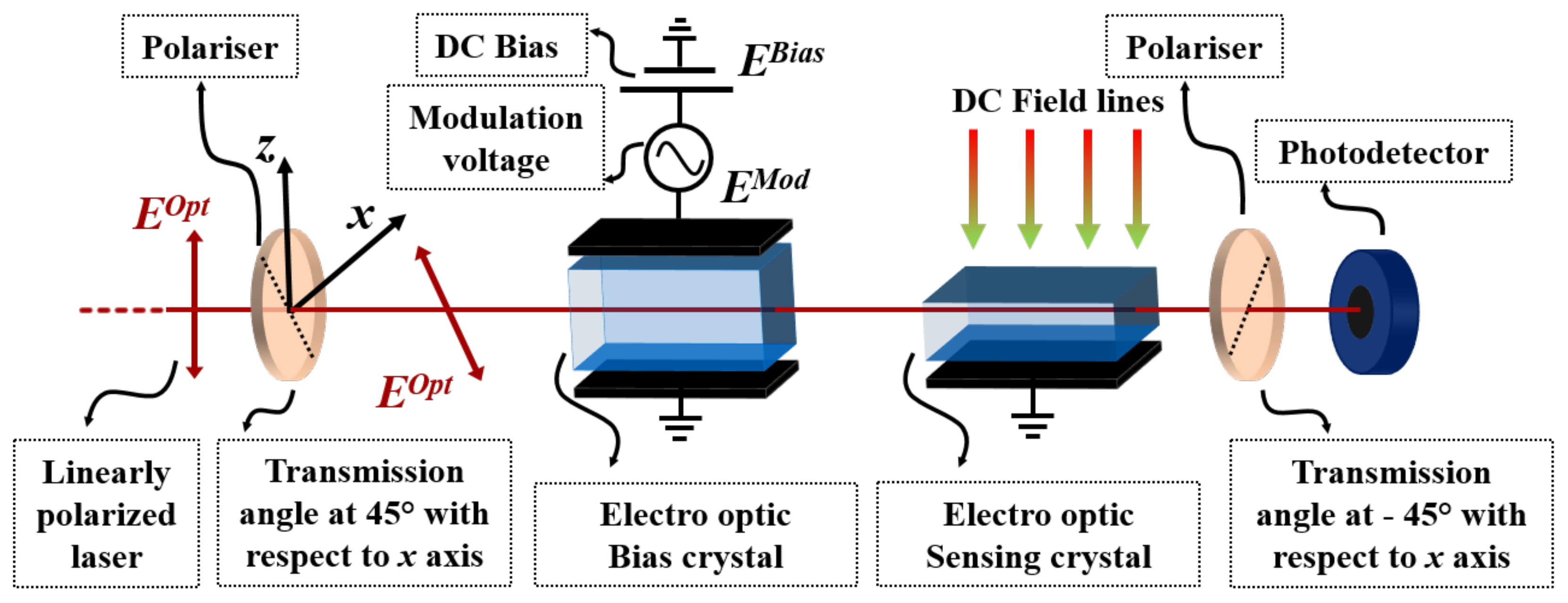
2.1. Electric Field Measurements with an Electro-Optic Sensor

The system is composed of two electro-optic (EO) crystals, made of Lithium Niobate (LiNbO3), and two polarizers arranged in a crossed-polarizers configuration. Large EO coefficients [2], as well as lower values of conductivity compared to the other EO materials [18], make LiNbO3 the preferred candidate to be used for electrostatic measurements.
To describe the sensor, we use the coordinate system shown in Figure 1.
The z-axis is parallel to the optical axis of a uniaxial LiNbO3 crystal. The refractive index along that direction is known as the extraordinary index (ne) and differs from the ordinary index (no), which is exhibited by the material along any other direction perpendicular to the optical axis. This material property is commonly referred to as birefringency [2].
Figure 2 presents a conceptual overview of an EO sensor for DC electric field measurements. A linearly polarized laser beam propagates in free space and traverses the entire optical chain. Using the aforementioned coordinate system, the laser beam propagates along the y-axis and oscillates in the perpendicular x-z plane.
The first polarizer fixes the light’s polarization at 45° with respect to the x-axis. As the laser beam enters the first crystal, two polarization components of the beam (orthogonal to the propagation direction) are unevenly phase-retarded due to the crystal’s natural birefringence, resulting in a different polarization state at the output face of the crystal. The laser beam undergoes the same phenomenon in the other crystal.
The second polarizer, set at −45° with respect to the x-axis, filters out the component of the laser beam not aligned with its transparency window, translating the polarization state change into a laser power variation. At the end of the optical chain, a photodetector measures the output optical power.
Because of the Pockels effect, EO crystal’s refractive indices change linearly with the incident electric field. The relationship between the electric field and crystal’s birefringence can be exploited to encode the incident electric field onto the polarization state of the laser beam traversing the crystals, resulting in an intensity modulation of the optical power.

2.2. Analytical Model

The mathematical model developed in MATLAB mimics the behavior of the optical chain shown in Figure 2 and was used for parametric simulations to find the optimal configuration for the test bench. Jones notation [19] was used to describe mathematically the components of the system and to evaluate the output signal. The optical beam propagates along y-axis and has components only in the x-z plane, therefore can be represented by the following polarisation vector:
E O p t ( t ) = E x O p t e i ( k y w t ) 0 E z O p t e i ( k y w t )
where k y w t is the phase of the light wave. In the specific case shown in Figure 2, the initial optical beam is characterized only by a component along z-axis. Moreover, the model exploits the normalised polarisation vector, which yields the following description of the optical beam:
E O p t ( t ) | E O p t ( t ) | = E N o r m O p t ( t ) = 0 1
All the other optical components are known elements of the Jones calculus and the electromagnetic wave that reaches the photodetector E O u t _ N o r m O p t can be computed as:
E O u t _ N o r m O p t ( t ) = 1 2 2 0 1 · 1 1 1 1 P o l a r i z e r · e i Γ b 2 0 0 e i Γ b 2 B i a s C r y s t a l · e i Γ s 2 0 0 e i Γ s 2 S e n s i n g c r y s t a l · 1 1 1 1 P o l a r i z e r
where the amplitude factor 1 2 2 comes from the analyser and the polariser. Particularly important are the factors of Γ b and Γ s , which represent the phase retardation Δ ϕ = ϕ x ϕ z between the two components E x and E z of the laser beam propagating through each crystal. The phase retardation between the two components of the optical beam is due to the birefringence of the EO crystals and is expressed as:
Γ = Δ ϕ = ϕ x ϕ z = 2 π λ ( n e n o ) L y
where λ is the wavelength of the optical beam and L y is the longitudinal dimension of the crystal. The Pockels effect results in a linear modulation of the refractive indices of the crystal. In Figure 2, both crystals experience an electric field only along z-axis. The first crystal (Electro-optic Bias crystal in Figure 2) is intentionally modulated with a sinusoidal modulation field offset by a DC component. The second crystal, or the sensing crystal, is instead used to couple the external electric field. Given the dependence of the refractive indices of L i N b O 3 from the electric field, Equation (4) can be expanded, taking into account the Pockels effect, and applied to the two crystals as:
Γ s = 2 π λ ( n e n o ) L y s N a t u r a l b i r e f r i n g e n c e π λ ( n e 3 r 33 n o 3 r 13 ) L y s [ E e x t ] P o c k e l s e f f e c t Γ b = 2 π λ ( n e n o ) L y b N a t u r a l b i r e f r i n g e n c e π λ ( n e 3 r 33 n o 3 r 13 ) L y b [ E m o d + E d c _ b i a s ] P o c k e l s e f f e c t
where r 33 and r 13 are the electro-optic coefficients of lithium niobate, E d c _ b i a s is the DC component of the bias voltage, E m o d = A sin ( 2 π f t ) is the sinusoidal modulation and E e x t is the field under measurement. To ease the notation, the dependence of the refractive indices and the electro-optic coefficients from the wavelength of the laser beam and the crystal’s temperature [20] are not written down explicitly. However, these dependencies have been taken into account in the mathematical model.
The final result of the matrices product in Equation (3) is:
E O u t _ N o r m O p t ( t ) = e i ( Γ b + Γ s ) 2 e i ( Γ b + Γ s ) 2 e i ( Γ b + Γ s ) 2 e i ( Γ b + Γ s ) 2
which simplifies, using Euler’s formula, to:
E O u t _ N o r m O p t ( t ) = i 2 sin ( Γ b + Γ s 2 ) sin ( Γ b + Γ s 2 )
Finally, since for complex field holds I = | E | 2 , the normalised intensity collected by the photodetector is:
I ( t ) = E O u t _ N o r m O p t , ( t ) · E O u t _ N o r m O p t ( t ) = sin 2 ( Γ b + Γ s 2 )
where E O u t _ N o r m O p t , ( t ) is the conjugate value of the normalized light wave on the output of the optical chain. Substituting the values of Γ b and Γ s from Equation (5), assuming constant E d c _ b i a s and collecting all the time invariant terms under a factor Γ 0 , Equation (8) is transformed into:
I ( t ) = sin 2 Γ 0 α ( A sin ( 2 π f t ) ) β ( E e x t )
where α = π λ ( n e 3 r 33 n o 3 r 13 ) L y b and β = α L y s L y b . The output intensity is then proportional to the function sin 2 ( sin ( x ) + ϕ ) , where the phase term is linearly proportional to the intentionally applied DC bias voltage and to the external electric field under measurement:
I ( t ) sin 2 ( sin ( 2 π f t ) + ϕ ( E d c _ b i a s , E e x t ) )
The analytical results shown in this paper are obtained by numerical computation of Equation (10).

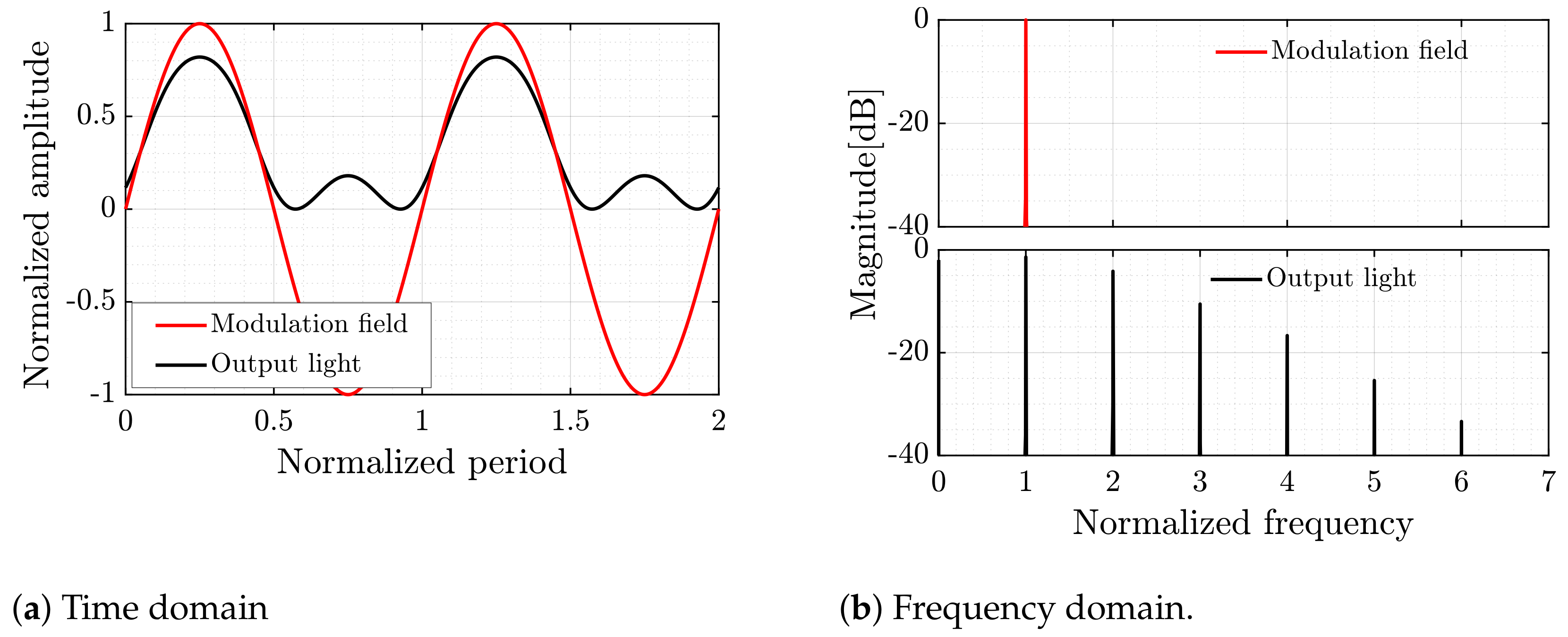
2.3. DC Measurement in the Frequency Domain

Figure 3 shows the system’s transfer function, obtained by sweeping the DC bias electric field acting on the bias crystal while measuring the relative output light intensity.
An important parameter of the crystals, annotated in Figure 3, is E π which is the electric field acting on the crystal for which the phase retardation between the two light components is δ = π . The value of E π is proportional to the optical beam wavelength λ and given by:
E π = λ L y n e 3 r 33 n o 3 r 13
where L y is the crystal’s length, n e and n o are the refractive indices, and r 13 and r 33 are the corresponding electro-optic coefficients.
Since it is a property of the crystal, we will distinguish between and E π B , for the bias crystal, and E π S , for the sensing crystal, as marked in Figure 2. Figure 3 shows the transfer function of the bias crystal with E π B being the electric field difference between the function’s consecutive minimum and maximum. Table 1 summarizes the properties of the crystals used for the simulations and in the developed test bench.
Conceptually, it is feasible to build the sensor with only a single EO crystal. However, using two separate crystals brings some practical advantages.
The first crystal can be placed further away from the incident electric field and be unaffected by it. Since the crystal is affixed between two Printed Circuit Boards (PCBs), it becomes possible to apply an arbitrary value of a static electric field, referred to henceforth as the DC bias. Such a solution allows us to fully control the system’s working point regardless of the incident electric field strength.
To perform DC measurements in the frequency domain, we supplement the DC bias with a sinusoidal modulation EMOD. The DC bias is chosen on purpose to exploit the symmetric shape of the transfer function at Working Point (WP) 1 or 2, as indicated in Figure 3. Sinusoidal modulation around either of these two points would result in an output signal containing only even (for WP1) or odd (for WP2) harmonics of the modulation frequency. Measurements of an incident field become possible by observing the change to the lowest harmonic, which is absent for a given WP, i.e., the first harmonic (H1) for WP1 and the second harmonic (H2) for WP2. The choice of working point, as well as the modulation’s frequency and amplitude, is discretionary and not physically limited by the sensor construction.
Modulation around WP1 (as well as the other crests and troughs of the transfer function) results in a higher sensitivity of the developed sensor. To explain the sensor’s principle of operation we assume a DC bias set to reach WP1 and a sinusoidal modulation with a peak-to-peak modulation amplitude E p p = E π B .
Figure 4 illustrates the system behaviour with no incident electric field on the sensing crystal. The horizontal axis is normalized by E π S to highlight the possibility of scaling the system’s sensitivity by varying the geometrical and physical properties of the crystals.
As the electric field across the bias crystal modulates, so does the output light intensity. However, due to the transfer function’s symmetry the latter happens at twice the modulation frequency, as shown in Figure 5a,b.
The two PCBs surrounding the bias crystal would unavoidably interact with the external electric field to be measured. Hence, the sensor features a second bare crystal (Electro-optic Sensing crystal in Figure 2) which can be placed close to the electric field of interest, encoding it onto the laser beam. The field acting on the sensing crystal effectively shifts the system’s working point which disrupts the transfer function’s symmetry, as shown in Figure 6 and Figure 7a. This makes odd harmonics appear in the frequency spectrum of the output signal as shown in Figure 7b.
With the sensing crystal exposed to an external electric field, odd harmonics of the modulation frequency appear in the output light intensity signal. In particular, the power of H1 increases proportionally with the external electric field intensity, as shown in Figure 8.

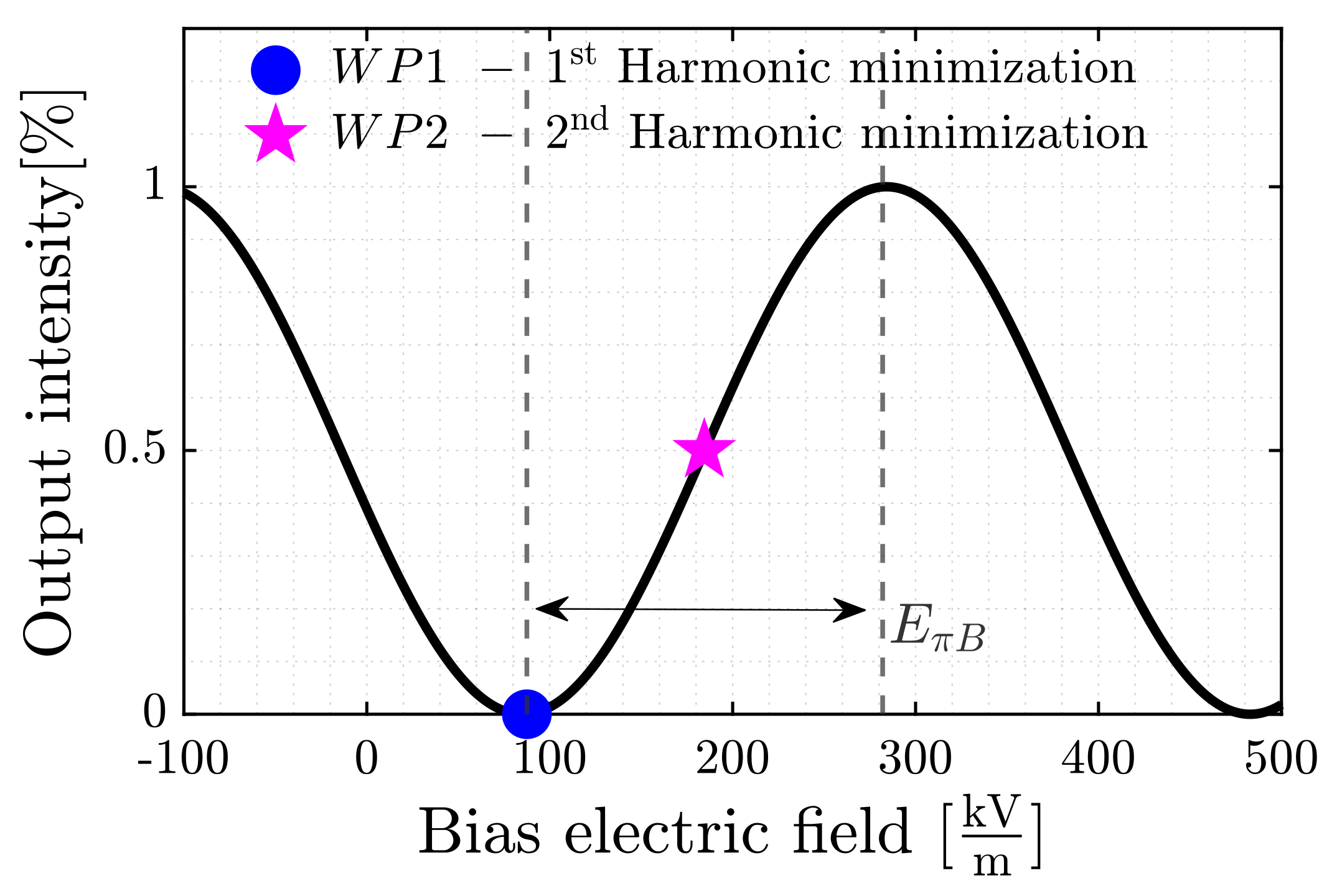
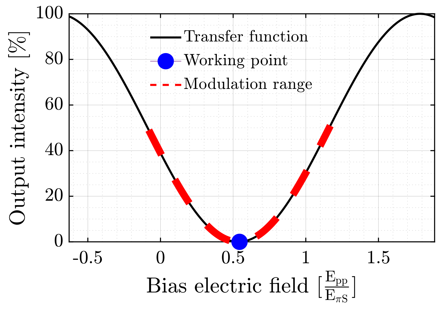
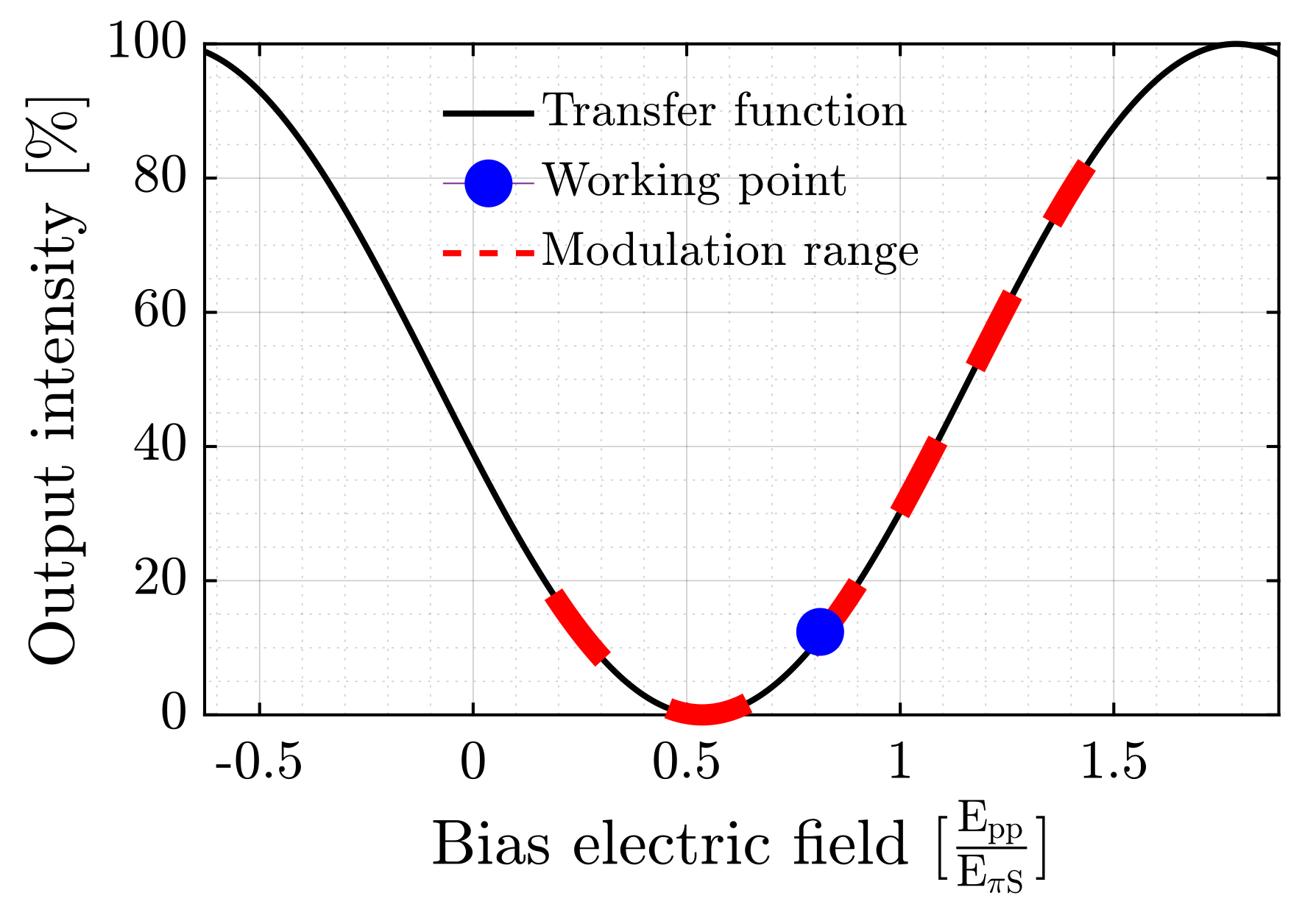
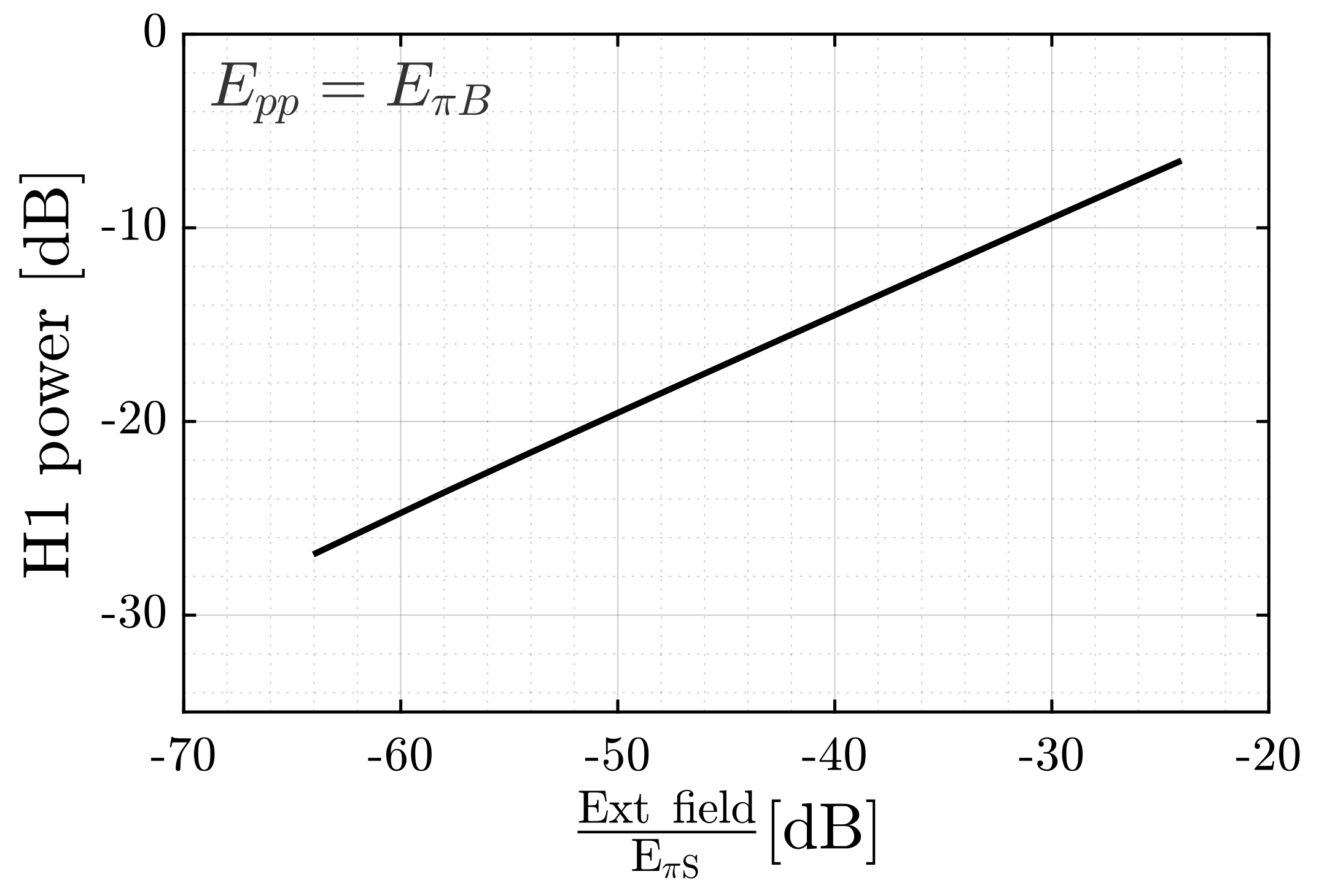
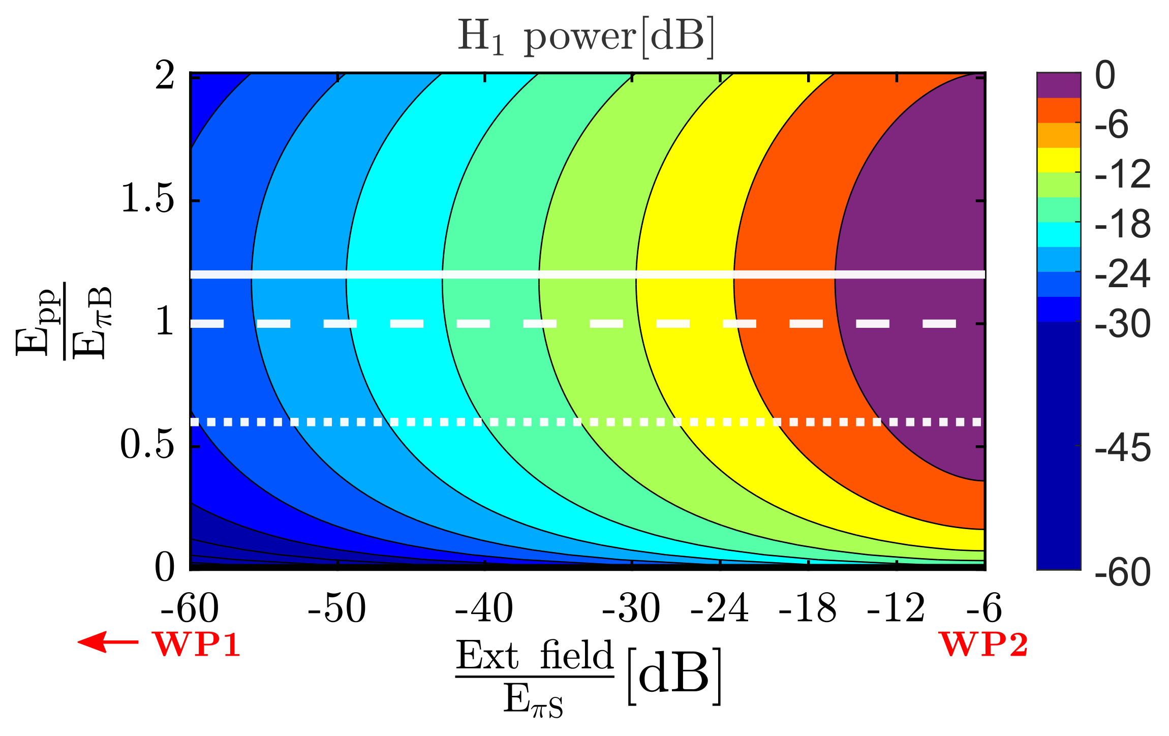
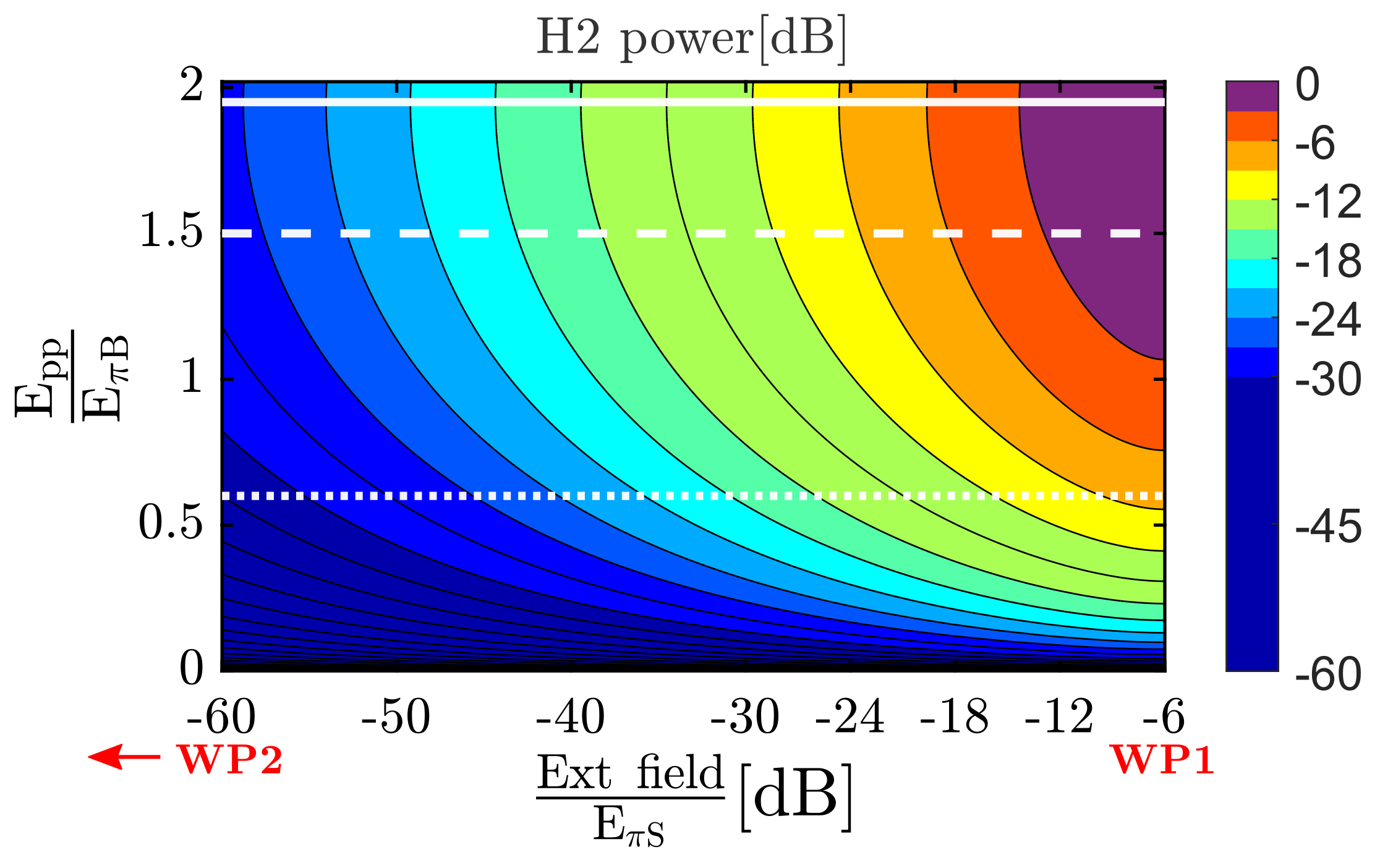
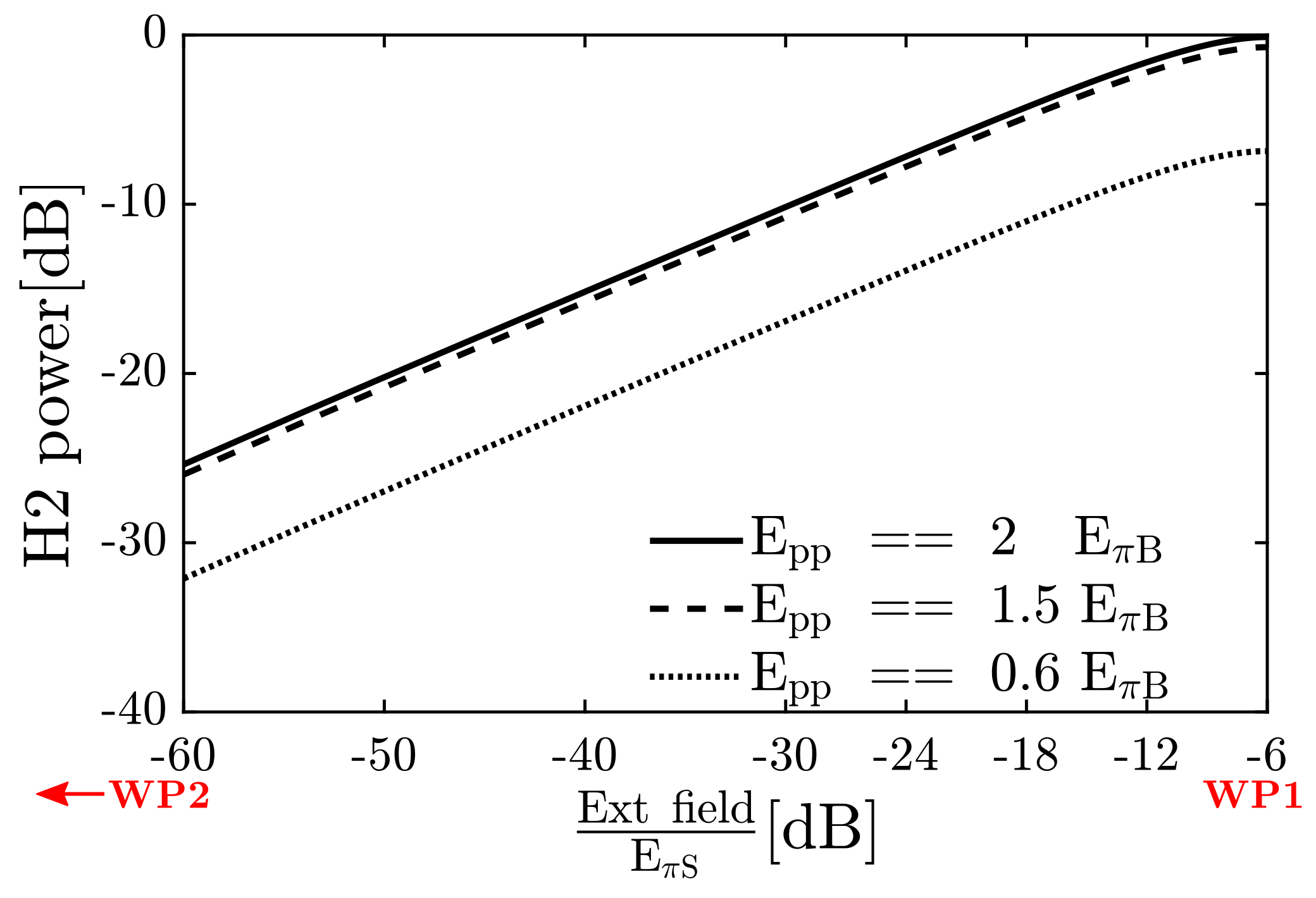
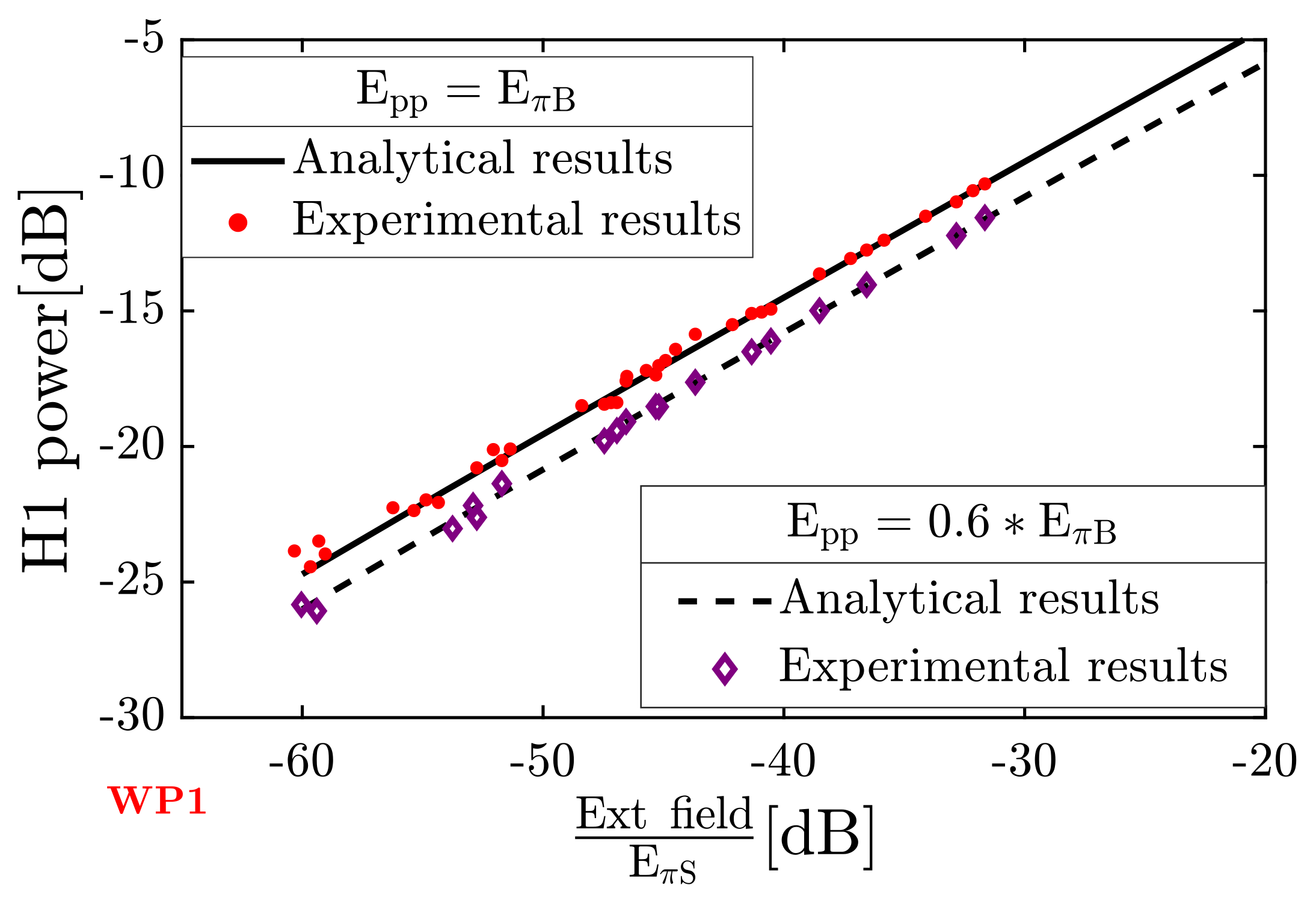
2.4. Choice of Working Point and Modulation Amplitude

With two available working points and a wide range of possible modulation amplitudes, selecting the operating conditions is a multi-dimensional problem. First, we consider both working points separately and find the optimal modulation amplitude for each.
Figure 9 shows the power of H1 with the sensor operating at WP1. The modulation amplitude ranges from 0 to 2 E π B , while the external field varies in the range from 0 to 0.6 E π S . H1 exhibits the highest power for E p p = 1.2 E π B and the external field magnitude of 0.5 E π S , with the latter being equivalent to moving from WP1 to WP2. Nevertheless, it is evident, that for any strength of the external field, the sensor reaches its peak sensitivity with E p p = 1.2 E π B .
Figure 10 shows the variation of the H1 power as a function of the external field for three values of amplitude modulation annotated with white lines in Figure 9. The slopes of the three curves are the same but modulation amplitudes lower than 1.2 E π B result in a lower power of H1. Figure 11 and Figure 12 show equivalent results obtained for H2 with the sensor operating at WP2.
As we present in Figure 13, which compares the results obtained using the optimal modulation amplitude for each working point, WP1 yields higher sensitivity for lower values of the amplitude modulation and is therefore the preferred configuration for operating the sensor.

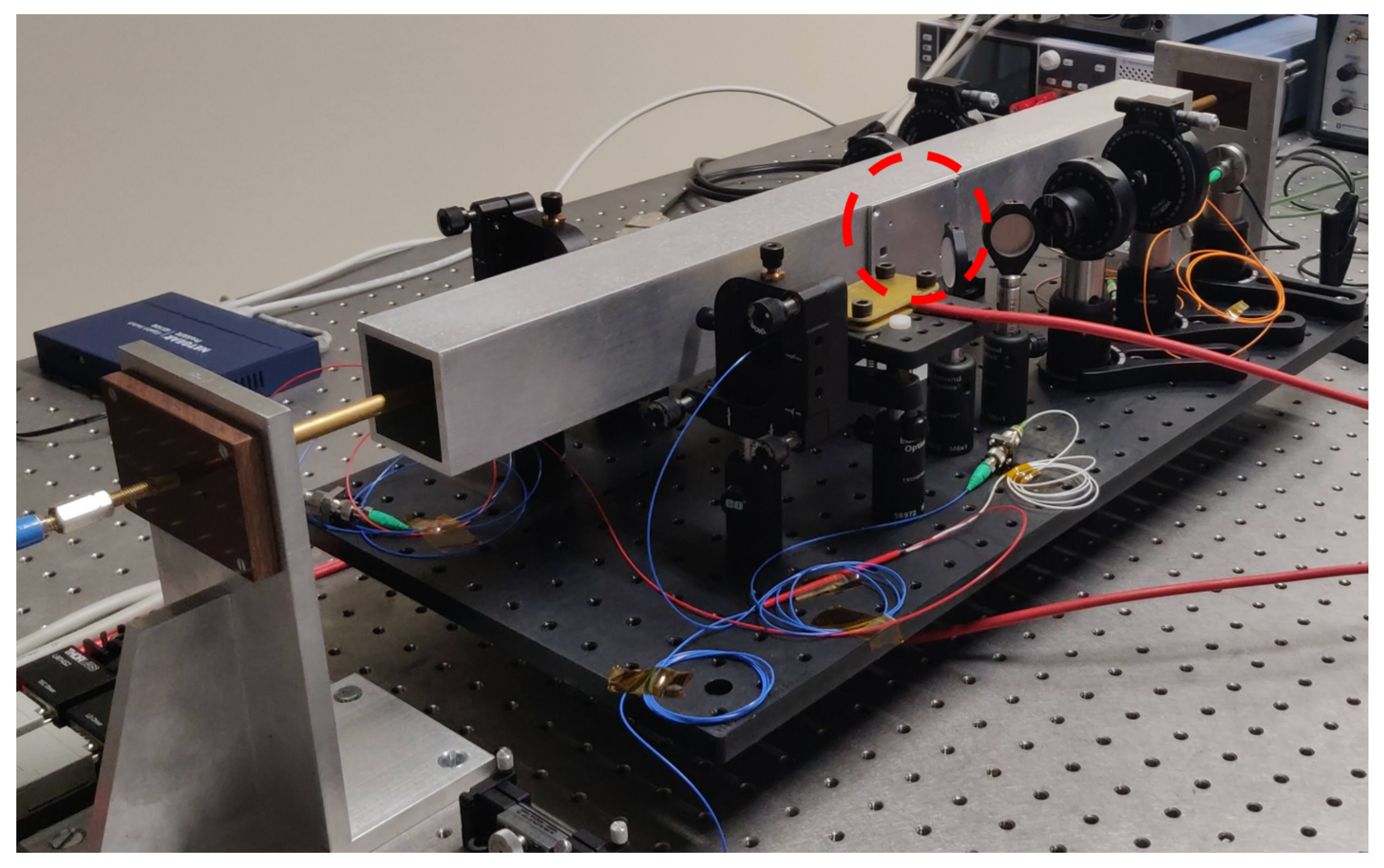
2.5. Proof-of-Concept Test Bench

The results obtained with the mathematical model served to design and optimize the proof-of-principle laboratory test bench. Given the ultimate objective of the project, the test bench resembles a particle accelerator vacuum chamber as shown in Figure 14.
The test bench consists of a 60 cm long pipe with a 45 × 45 mm square aperture which houses the electric-field-sensing crystal (i.e., the second crystal in the previously described mathematical model) which is attached to a removable holder—annotated with a red circle in Figure 14) and shown in detail in Figure 15. The holder is installed on the horizontal wall of the pipe. The sensing crystal is a 50 mm long, unpoled and uncoated LiNbO3 crystal, doped with MgO at 5% and has a cross section of 2 × 5 mm.
Two metal stripes attach the crystal to the metal holder, lowering the electric field intensity in the crystal. The attenuation, evaluated through numerical electrostatic simulations of the test bench, is stronger by approximately 32% compared to an equivalent dielectric holder. This effect was known during the design phase of the sensor but a metal holder was used nevertheless to ease fabrication of the test bench. Moreover, the ultimate goal of our development is to apply the proposed technique to measure the relative strength of two electric fields using two sensors placed symmetrically around the centre of the field source. As such measurements do not require knowing the absolute field intensity, the final choice was to produce the holder out of metal.
The bias crystal is made from the same material as the sensing crystal but is 40 mm long, with a cross section of 3 × 3 mm. Additionally, to improve electric contact with the PCBs, the bias crystal features a Cr-Au coating on the two sides parallel to the z-plane.
The bias crystal is fixed outside of the square pipe, between two PCBs connected to a high-voltage piezo-amplifier (SVR 1000/3 from PIEZOSYSTEM JENA). The entire optical chain was assembled using off-the-shelf THORLABS components.
First, a single frequency, linearly polarized, laser diode (SFL1550P) generates the laser beam which travels through a polarization-maintaining fiber to a collimator (CPF5-1550A) which maintains the laser beam’s polarization. By rotating the collimator, it is possible to fix a 45 polarization on the input face of the bias crystals without using a dedicated polarizer. After traversing the bias crystal, the laser beam is guided in and out of the sensing crystal holder by two mirrors (PF10-03-P01) and two prisms. The laser beam then couples into a Glan-Taylor polarizer (GT10-C).
Finally, a photodetector (S122C) connected to a power meter (PM100D) provides an output signal which is measured by a 10-bit oscilloscope and a signal analyzer. The SL1550P laser diode generates a single-frequency laser beam with a wavelength of 1550 nm. This choice, even if counter intuitive considering the figure of merit E π in Equation (11), was made to minimize the creation of optically induced hole-electron pairs, since the absorption coefficient in LiNbO3 is at its lowest value [21] for that wavelength. Moreover, an abundance of commercially available optical components and detectors for the 1550 nm wavelength commonly used by the telecommunications industry made our proof-of-principle development faster and cheaper.
The electric field measured by the sensing crystal is radiated by a rigid wire, traversing the entire square pipe, to which a voltage up to 1 kV can be applied. The length of the pipe and wire are large compared to the crystal’s length which enables a uniform distribution of electric field close to the sensing crystal. The pipe and optical components are fixed on an optical breadboard mounted on a motorized, linear translation stage which, in turn, is connected to a large optical table. The breadboard can move along one direction around the stationary wire that is attached to the large optical table. This last feature will be used in the future to assess the feasibility of the sensor to measure transverse displacement of the electric field source.
The first experimental results were obtained exploiting the working point WP1 and two different modulation amplitudes, E p p = E π and E p p = 0.6 E π , in order to validate the analytical results. Figure 16 compares the laboratory measurements with the analytical results showed previously in Figure 8. The chosen modulation frequency of 600 Hz was far from the piezoamplifier limit to avoid errors on the measurement due to modulation distortion. The oscilloscope recorded the output signal at a 100 kHz sampling rate.
The sensor measured an electric field ranging from 3 to 150 kV/m, limited at the lower end by the dynamic range of the acquisition system, and at the higher end by the maximum voltage we could apply to the rod.

2.6. Possible Sources of Measurement Error

The experimental observations shown in the previous section match the analytical predictions well, with higher field intensity yielding more accurate results. The discrepancy for low values of the electric field can be explained by multiple factors discussed in the following paragraphs.

2.6.1. Space Charge Build-Up

Space charge on the boundaries of an EO crystal increases exponentially due to a DC or quasi-DC electric field acting on the crystal. The macroscopic internal electric field, which is also responsible for the Electro-Optic effect, follows Equation [18,22]:
E i n = E e x t ϵ r e t τ
where E i n is the internal electric field, E e x t is the DC external field, ϵ r is the dielectric permittivity of the electro-optic material and τ = ϵ o ϵ r σ is the relaxation time constant that depends on the dielectric permittivity of the material and its conductivity.
The movement of the free charge carriers to the boundaries affects both of the sensor’s crystals. The charge build-up in the bias crystal is due to the applied DC bias voltage. The variation of the internal electric field can be compensated by tuning the sensor and varying the DC component of the bias voltage.
The space charge effects in the sensing crystal can not be compensated through the proposed scheme and it is difficult to quantify their impact on the measurement accuracy since they coincide with other parasitic effects such as temperature-related drifts. However, the sensor was designed to minimize the build-up of the charge through several means:
  • Following Equation (12), the charge build-up and decay depend on the relaxation time of the material and, therefore, on its conductivity. Lithium Niobate exhibits the highest time constant among common EO materials ( 10 5 s) which in principle allows steady EO conditions in a large time window relative to the measurement time. From Equation (12), the internal electric field in a LiNbO 3 crystal decays by 1% after almost 17 min.
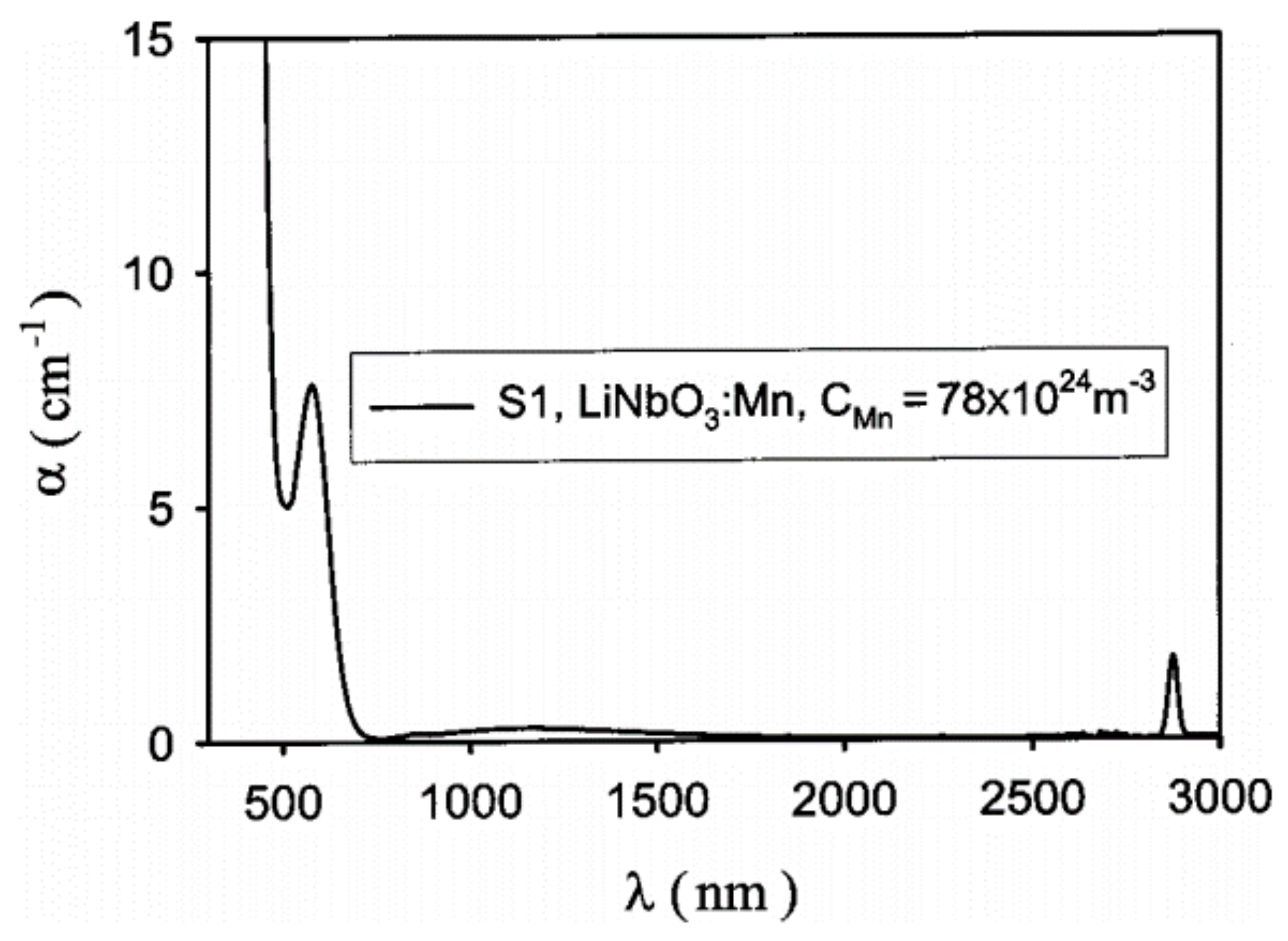
  • Since the build-up of space charge is caused by free charge carriers, it is important to avoid effects which could increase the number of free carriers. The photorefractive effect excites electrons to the conduction band and also leads to a variation of the material’s refractive indices. The rate of excitation depends on the wavelength of the laser beam passing through the crystal. Figure 17 shows the absorption coefficient of L i N b O 3 doped with manganese at different concentration levels.
    While some peaks are caused by the used dopant, the remaining characteristic is due to the properties of L i N b O 3 , showing an almost zero absorption coefficient at 1550 nm.
    The crystals used in the developed sensor are doped with magnesium oxide and not manganese. However, the lack of literature regarding the energy levels of defects introduced through magnesium oxide doping at wavelengths out of the visible light range suggests that the defects are located only in that range. Therefore, the wavelength of the laser beam chosen for the presented sensor is 1550 nm.

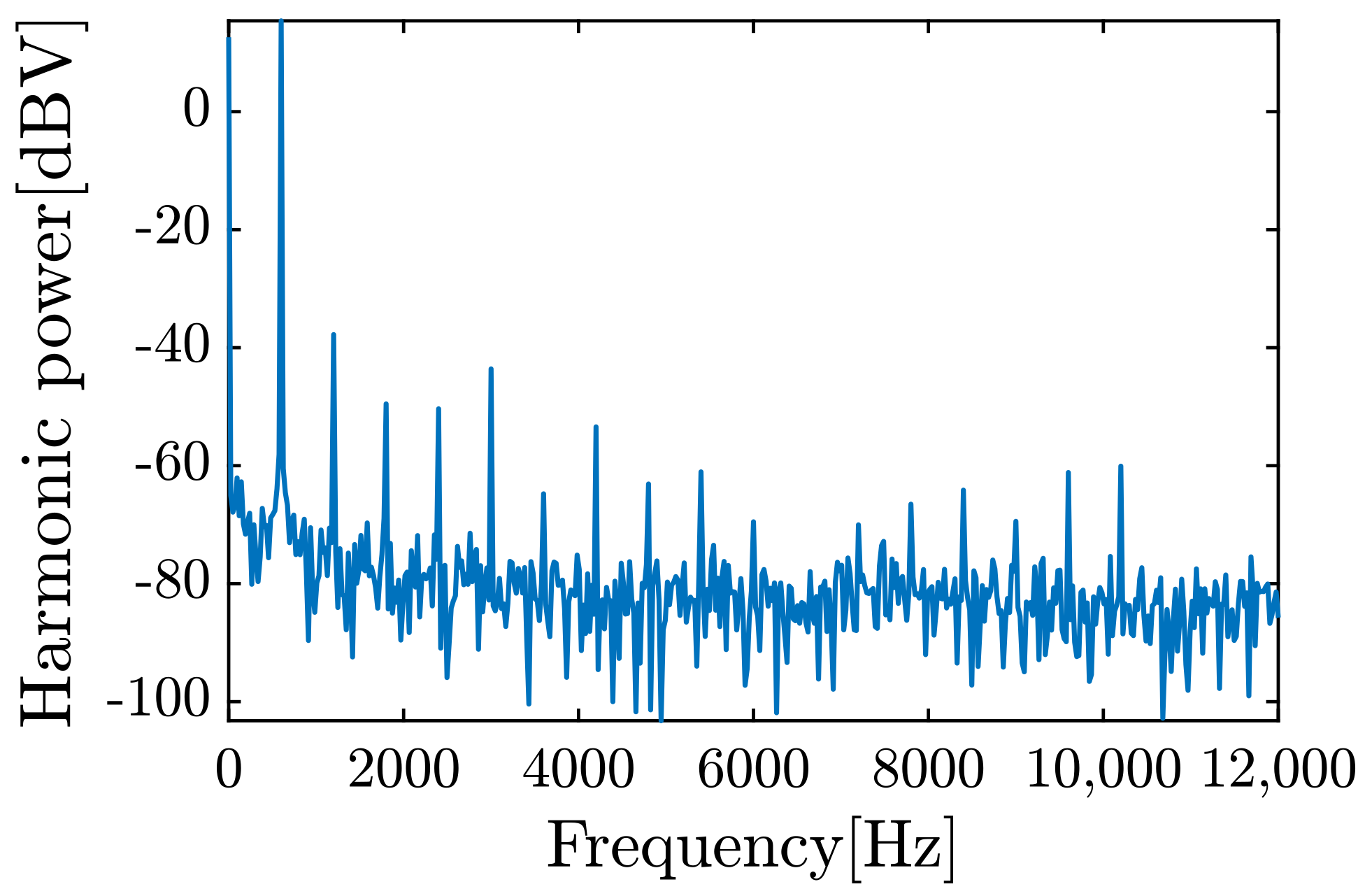
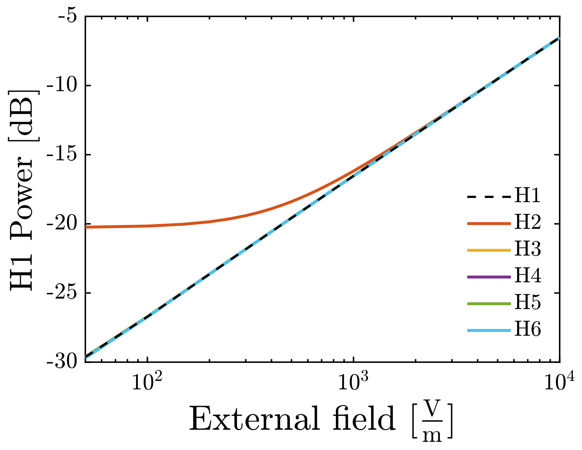
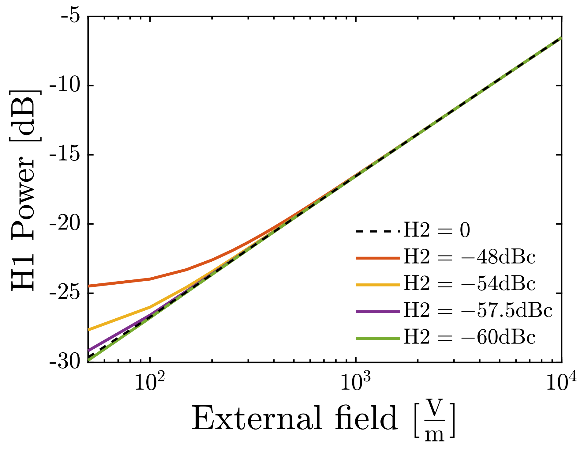
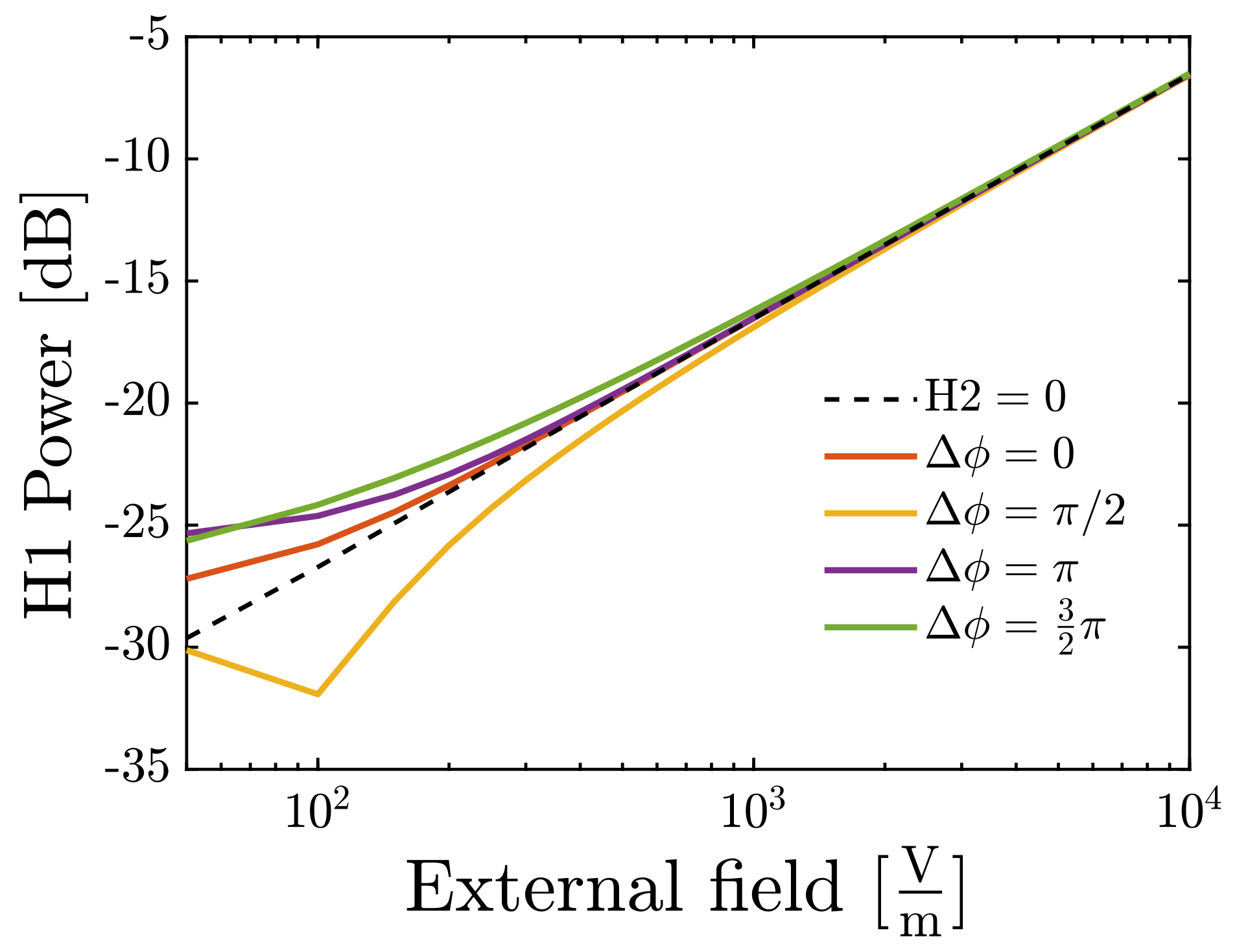
2.6.2. Imperfect Modulation Source

As the sensor encodes the measured field intensity onto a particular harmonic of the modulation frequency, spurious harmonics of the modulation source can affect the measurement accuracy. Figure 18 shows the power spectral density of the modulation signal applied to the bias crystal, which is assumed to be a pure high-amplitude 600 Hz sine wave.
The second harmonic at f = 1200 Hz is the prevalent spurious component, with its amplitude lower by 53 dB, or a factor of 450 , relative to the fundamental component.
Numerical simulations were used to evaluate the impact of various spurious harmonics on the measurement accuracy. The simulated modulation signal was a superposition of a pure sine wave at the fundamental frequency and a 100 times smaller sine wave at one of the higher harmonics.
Figure 19 shows that only the second harmonic has a strong impact on the measurement accuracy which becomes evident for measured field intensities below 1 kV/m. Therefore, further analysis focuses on this harmonic only. In particular, the impact of its amplitude and the phase difference with respect to the fundamental harmonic are evaluated.
Figure 20 and Figure 21 show, respectively, the effects of the second harmonic amplitude and phase offset with respect to the fundamental frequency on the measurement accuracy. The results are benchmarked against modulation with a pure sinusoidal signal, i.e., H 2 = 0 .
The effects are not negligible, especially for low values of the electric field to measure, making the spurious harmonics on the applied modulation signal a very plausible explanation for the error observed in experimental measurements of low electric fields.
However, since the output remains a unique function of the electric field, both of these errors can be corrected by data postprocessing, once the system is calibrated prior to the measurement.

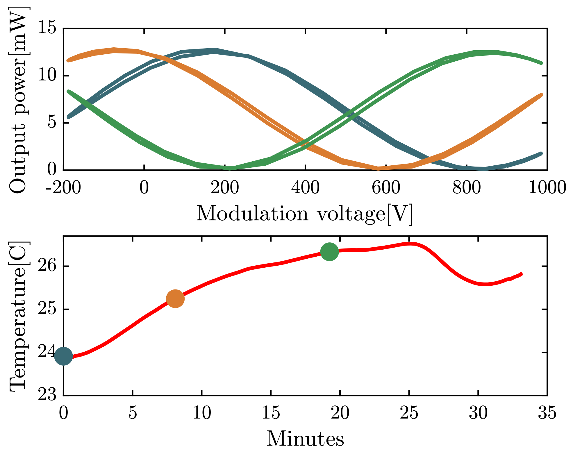
2.6.3. Temperature Drift

Temperature variations affect birefringence. As the sensor’s two crystals are installed in two different locations, they might be exposed to different temperatures which is equivalent to an additional phase retardation. This shifts the sensor’s transfer function but it does not impact its amplitude. Figure 22 and Figure 23 show experimental data taken in a climate chamber where the transfer function of the system is evaluated at different temperatures, equal to the colored dots in the temperature plots, for a rising and then falling temperature. The transfer function at a given temperature is linked by the color of the plot to the related temperature.
Since the process is relatively slow compared to the foreseen measurement time, which is in the order of seconds, temperature drifts are unlikely to have resulted in a significant measurement error. However, during the initial tuning of the sensor, the effect is easily compensated by adjusting the DC bias voltage, regardless of the temperature difference between the two crystals.

3. Conclusions

We have presented a novel electro-optic sensor optimized for measurements of DC electric fields in a harsh environment, such as a particle accelerator. The sensor is composed of a chain of two EO crystals; one crystal placed close to the field to be measured, and another crystal exploited to continuously tune the sensor with a bias voltage, and to apply a modulation voltage allowing DC measurement to be performed in the frequency domain.
Theoretical analysis and experimental results confirm the feasibility of the proposed detection technique. The method can by applied to a wide range of electric field intensities by scaling the EO crystals’ dimensions.
Further improvements are under investigation. In particular, a custom acquisition chain based on a VFC acquisition card developed at CERN [23] and a 24-bit ADC/DAC module is under development to improve the sensitivity of the system.
We aim to enhance the dynamic range on the first harmonic power evaluation from the current 40 dB. Our analysis indicated that an improved acquisition chain will extend the dynamic range to more than 80 dB, leading to an improvement of over four orders of magnitude. The increased resolution and speed of the system will also open the possibility of studying in detail the impact of other parasitic effects experience by EO crystals, as temperature drift and space charge, on the measurement quality.

Author Contributions

Conceptualization, M.K. and A.C.; formal analysis, A.C.; Visualization, A.C.; writing—original draft preparation, A.C.; writing—review and editing, M.K. and R.H.; supervision, M.K. and R.H.; funding acquisition, M.K. All authors have read and agreed to the published version of the manuscript.

Funding

This project has received funding from the ATTRACT project funded by the EC under Grant Agreement 777222.

Acknowledgments

The authors express their gratitude to Juan Carlos Allica Santamaria, Franck Guy Guillot-Vignot, Patrick Bouvier, Morad Hamani, Thibaut Lefevre, Stefano Mazzoni, and Romain Ruffieux from the Beam Instrumentation Group at CERN, and Alberto Arteche from Royal Holloway University of London, for their help with the design and construction of the EO test bench and for the commissioning of the laser lab.

Conflicts of Interest

The authors declare no conflict of interest.

Abbreviations

The following abbreviations are used in this manuscript:
EOElectro-optic
DCDirect current
BPMBeam position monitor
SHiPSearch for Hidden Particles
WPWorking point

References

  1. Duvillaret, L.; Rialland, S.; Coutaz, J.L. Electro-optic sensors for electric field measurements. II. Choice of the crystals and complete optimization of their orientation. JOSA B 2002, 19, 2704–2715. [Google Scholar] [CrossRef]
  2. Weis, R.; Gaylord, T. Lithium niobate: Summary of physical properties and crystal structure. Appl. Phys. A 1985, 37, 191–203. [Google Scholar] [CrossRef]
  3. Herres, D. Understanding Electro-Optic Modulation. Available online: https://www.testandmeasurementtips.com/understanding-and-measuring-electro-optic-modulation-faq/ (accessed on 24 July 2022).
  4. Okayasu, Y.; Tomizawa, H.; Matsubara, S.; Sato, T.; Ogawa, K.; Togashi, T.; Takahashi, E.; Minamide, H.; Matsukawa, K.; Aoyama, M.; et al. The First Electron Bunch Measurement by Means of DAST Organic EO Crystals. Available online: https://jopss.jaea.go.jp/search/servlet/search?5040292 (accessed on 24 July 2022).
  5. Wu, Q.; Zhang, X.C. Ultrafast electro-optic field sensors. Appl. Phys. Lett. 1996, 68, 1604–1606. [Google Scholar] [CrossRef]
  6. Shen, Y.; Carr, G.; Murphy, J.B.; Tsang, T.Y.; Wang, X.; Yang, X. Electro-optic time lensing with an intense single-cycle terahertz pulse. Phys. Rev. A 2010, 81, 053835. [Google Scholar] [CrossRef]
  7. Wilke, I.; MacLeod, A.M.; Gillespie, W.A.; Berden, G.; Knippels, G.; Van Der Meer, A. Single-shot electron-beam bunch length measurements. Phys. Rev. Lett. 2002, 88, 124801. [Google Scholar] [CrossRef] [PubMed]
  8. Berden, G.; Jamison, S.P.; MacLeod, A.M.; Gillespie, W.A.; Redlich, B.; Van der Meer, A. Electro-optic technique with improved time resolution for real-time, nondestructive, single-shot measurements of femtosecond electron bunch profiles. Phys. Rev. Lett. 2004, 93, 114802. [Google Scholar] [CrossRef] [PubMed]
  9. Pan, R. Electro-optic Diagnostic Techniques for the CLIC Linear Collider. Ph.D. Thesis, University of Dundee, Dundee, UK, 2015. [Google Scholar]
  10. Wendt, M. BPM systems: A brief introduction to beam position monitoring. arXiv 2020, arXiv:2005.14081. [Google Scholar]
  11. Doherty, J. The Electro-Optic Beam Position Monitor; Technical Report; Open University: Oxford, UK, 2013. [Google Scholar]
  12. Gibson, S.; Bosco, A.; Lefèvre, T.; Arteche, A.; Boorman, G.; Levens, T.; Darmedru, P.Y. High frequency electro-optic beam position monitors for intra-bunch diagnostics at the LHC. In Proceedings of the International Beam Instrumentation Conference, Melbourne, Australia, 13–17 September 2015. [Google Scholar]
  13. Kuwabara, N.; Tajima, K.; Kobayashi, R.; Amemiya, F. Development and analysis of electric field sensor using LiNbO3 optical modulator. IEEE Trans. Electromagn. Compat. 1992, 34, 391–396. [Google Scholar] [CrossRef]
  14. Cecelja, F.; Bordovsky, M.; Balachandran, W. Electro-optic sensor for measurement of DC fields in the presence of space charge. IEEE Trans. Instrum. Meas. 2002, 51, 282–286. [Google Scholar] [CrossRef]
  15. Liu, J.; Wang, H.; Li, Y. Research and Design of Rotary Optical Electric Field Sensor. In IOP Conference Series: Materials Science and Engineering; IOP Publishing: Bristol, UK, 2019; Volume 677, p. 052112. [Google Scholar]
  16. Miles, R.; Bond, T.; Meyer, G. Report on Non-Contact DC Electric Field Sensors; Technical Report; Lawrence Livermore National Lab. (LLNL): Livermore, CA, USA, 2009. [Google Scholar]
  17. Ahdida, C.; Alia, R.; Arduini, G.; Arnalich, A.; Avigni, P.; Bardou, F.; Battistin, M.; Bauche, J.; Brugger, M.; Busom, J.; et al. SPS Beam Dump Facility–Comprehensive Design Study. arXiv 2019, arXiv:1912.06356. [Google Scholar]
  18. Cecelja, F.; Balachandran, W.; Bordowski, M. Validation of electro-optic sensors for measurement of DC fields in the presence of space charge. Measurement 2007, 40, 450–458. [Google Scholar] [CrossRef]
  19. Jones, R.C. A new calculus for the treatment of optical systemsi. description and discussion of the calculus. Josa 1941, 31, 488–493. [Google Scholar] [CrossRef]
  20. Schlarb, U.; Betzler, K. Refractive indices of lithium niobate as a function of temperature, wavelength, and composition: A generalized fit. Phys. Rev. B 1993, 48, 15613. [Google Scholar] [CrossRef] [PubMed]
  21. Yang, Y.; Psaltis, D.; Luennemann, M.; Berben, D.; Hartwig, U.; Buse, K. Photorefractive properties of lithium niobate crystals doped with manganese. JOSA B 2003, 20, 1491–1502. [Google Scholar] [CrossRef]
  22. Seaver, A.E. An equation for charge decay valid in both conductors and insulators. arXiv 2008, arXiv:0801.4182. [Google Scholar]
  23. Boccardi, A.; Barros Marin, M.; Levens, T.; Szuk, B.; Viganò, W.; Zamantzas, C. A modular approach to acquisition systems for future CERN beam instrumentation developments. In Proceedings of the 15th International Conference on Accelerator and Large Experimental Physics Control Systems, Melbourne, Australia, 17–23 October 2015. [Google Scholar]
Figure 1. Coordinate system used throughout the paper.
Applsci 12 08544 g001
Figure 2. Schematic overview of the EO sensor for measurements of a DC electric field.
Applsci 12 08544 g002
Figure 3. Transfer function of the system.
Applsci 12 08544 g003
Figure 4. Range of modulation around the working point with no electric field incident on the second crystal.
Applsci 12 08544 g004
Figure 5. EMOD and output light intensity with no electric field incident on the second crystal.
Applsci 12 08544 g005
Figure 6. Range of modulation around the working point shifted by an electric field incident on the second crystal.
Applsci 12 08544 g006
Figure 7. EMOD and output light with an electric field incident on the second crystal.
Applsci 12 08544 g007
Figure 8. H1 power as a function of the incident electric field.
Applsci 12 08544 g008
Figure 9. H1 power as a function of the external electric field and modulation amplitude. The solid, dashed and dotted lines indicates H1 power at constant amplitude modulation E p p = 2 , 1.5 , 0.6 E π B .
Applsci 12 08544 g009
Figure 10. H1 power as a function of the incident electric field for fixed values of the modulation amplitude.
Applsci 12 08544 g010
Figure 11. H2 power as a function of the external electric field and modulation amplitude. The solid, dashed and dotted lines indicates H2 power at constant amplitude modulation E p p = 2 , 1.5 , 0.6 E π B .
Applsci 12 08544 g011
Figure 12. H2 power as a function of the incident electric field for fixed values of the modulation amplitude.
Applsci 12 08544 g012
Figure 13. Comparison of the two most sensitive combinations of working point and modulation amplitude.
Applsci 12 08544 g013
Figure 14. Proof-of-principle laboratory test bench. The red circle highlights the metallic holder used for the sensing crystal.
Applsci 12 08544 g014
Figure 15. Sensing crystal holder.
Applsci 12 08544 g015
Figure 16. Comparison of the experimental and analytical results.
Applsci 12 08544 g016
Figure 17. Absorption coefficient of L i N b O 3 doped with manganese [21].
Applsci 12 08544 g017
Figure 18. Power spectral density of the modulation voltage.
Applsci 12 08544 g018
Figure 19. Impact of the first 5 spurious harmonics on the measurement accuracy compared to the fundamental harmonic. The amplitude of each harmonics was 1% of the fundamental frequency amplitude.
Applsci 12 08544 g019
Figure 20. Impact of the spurious second harmonic amplitude on the measurement accuracy. H2 amplitude is referred to the fundamental frequency amplitude.
Applsci 12 08544 g020
Figure 21. Impact of the phase difference between the spurious second harmonic and the fundamental frequency. The calculations were done for H2 = −54 dBc.
Applsci 12 08544 g021
Figure 22. Shift of the transfer function due to rising temperature.
Applsci 12 08544 g022
Figure 23. Shift of the transfer function due to decreasing temperature.
Applsci 12 08544 g023
Table 1. Properties of the crystals used in the EO sensor.
 Bias CrystalSensing Crystal
Material L i N b O 3 (5% M g O doped)
Lx [mm]35
Ly [mm]4050
Lz [mm]32
E π [ kV m ]159203.9
Publisher’s Note: MDPI stays neutral with regard to jurisdictional claims in published maps and institutional affiliations.

