1. Introduction
An ultra-wideband (UWB) technique has drawn continuous attention in a broad range of applications since its standardization in 2002 [
1]. The allocated frequency range of UWB is 3.1 GHz to 10.6 GHz with a channel bandwidth of more than 500 MHz (absolute bandwidth) or 20% (fractional bandwidth). Due to this large bandwidth, UWB offers high-data-rate communications and high-resolution sensing/imaging in a variety of applications such as radar/detection systems, localization/positioning systems, wireless communications networks, medical imaging, etc. [
2,
3,
4,
5,
6].
Recently, there has been a strong demand for applying an Impulse Radio UWB (IR-UWB) technique thanks to the use of a low-power ultra-short pulse (sub-nanosecond interval) in a very low duty cycle (less than 0.5 percent) for the transmission and reception of information. For instance, [
7] proposes an IR-UWB radar operating at a center frequency of 6.8 GHz for identifying the vital signs of stationary/non-stationary humans, and [
8] presents a 4.3 GHz IR-UWB radar that can sense a target through foliage and through walls. In [
9], a brain-implanted antenna for a 4 GHz IR-UWB transmitter is proposed for delivering brain signals to an out-of-brain receiver with a high data rate.
In this paper, we propose a design of antenna array for an IR-UWB radar for the detection of human vital signs [
10]. The target is to design a 2 × 2 planar array operating at the center frequency of 7.5 GHz with a bandwidth of 800 MHz (7.1–7.9 GHz) in a small-area printed circuit board (PCB) of 36 mm × 40 mm. The reason for designing the antenna array instead of a single antenna is to enhance the antenna gain and reduce the antenna beamwidth; thus, the longitudinal detection range can be improved without detecting unwanted clusters in the transverse direction. However, designing four antennas (i.e., 2 × 2) in the given area (i.e., 36 × 40 mm
2) is challenging since the wavelength of the lowest frequency (i.e., 7.1 GHz) is already 42.2 mm. Therefore, it is necessary to adopt an antenna array miniaturization technique to include multiple antennas and their feed lines in the limited space. In the proposed design, a co-operate feed network is used to pack four antennas in a limited footprint. Furthermore, an antenna bandwidth broadening technique is call for to secure 800 MHz of bandwidth. In previous literature, a defected ground structure [
11], monopole [
12], U-slot [
13], and slot line-fed microstrip [
14] techniques have been proposed. In this work, two slots are simply designed in the antenna to divert the currents and to introduce a secondary resonance for bandwidth enhancement.
In what follows,
Section 2 outlines the design and optimization of a single antenna and the two-slot bandwidth enhancement technique. Based on the optimized single antenna,
Section 3 expands the design to a 2 × 2 antenna array. The PCB layouts of the radiator and feed are explained in detail, and the array simulation performance is analyzed and discussed. Having acquired the optimized antenna array design, a couple of prototypes were fabricated, and their measurement results are summarized in
Section 4. The measured results show that the antenna array is operating well at the target bandwidth of 7.1–7.9 GHz, and the half-power beamwidth (HPBW) is limited around 40–50° with a high gain up to 8.4 dBi.
Section 5 concludes the paper.
2. Single Antenna Design
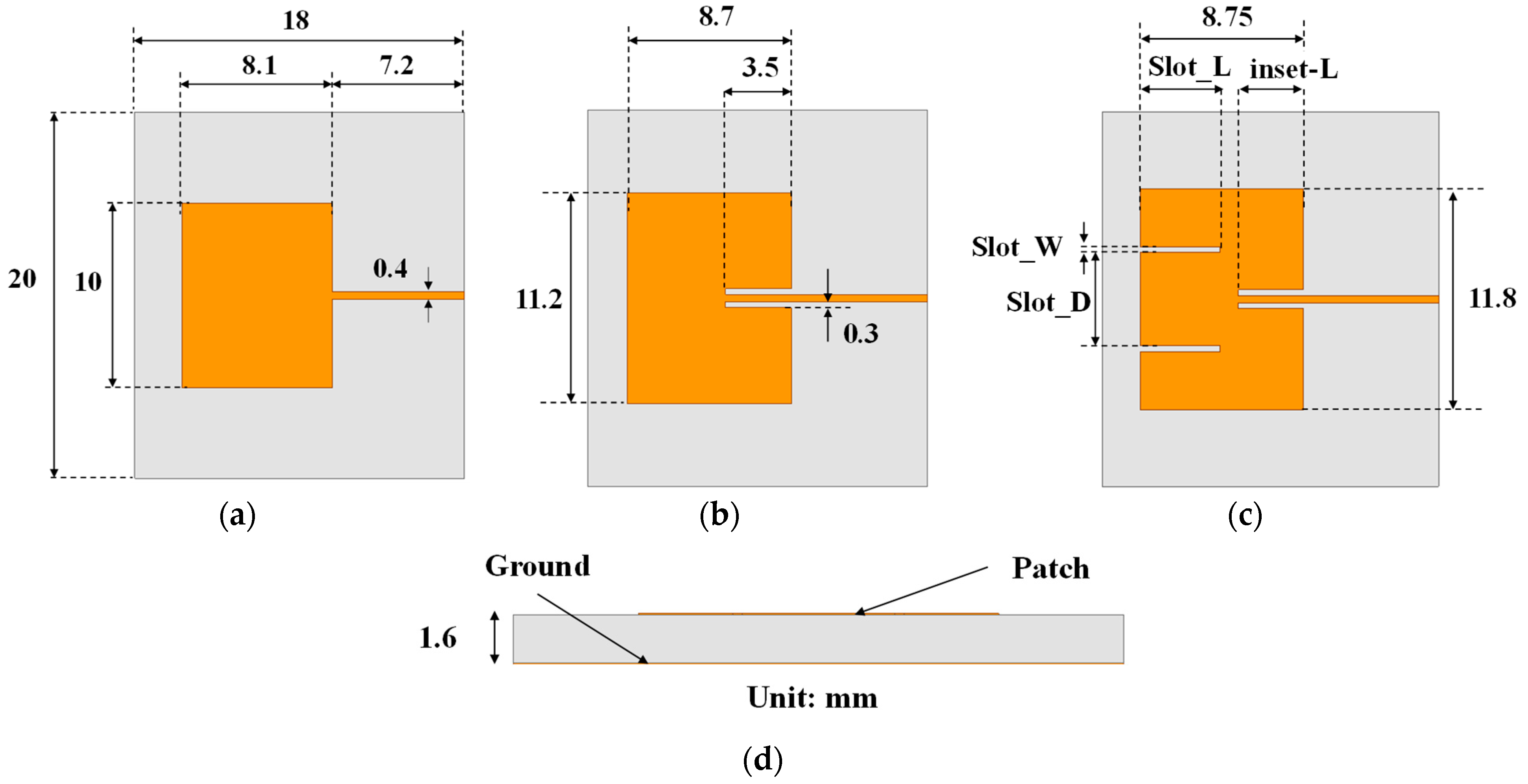
Figure 1 shows three geometrical designs of a single antenna, which are: conventional patch, inset-fed patch, and inset-fed and two-slot patch antennas, from left to right, respectively. All three geometries use the microstrip printed circuit board (PCB) technique, such as in
Figure 1d. The entire circuit is based on the design of a signal processing circuit for an IR-UWB radar application and is constructed on an FR-4 four-layer stack-up substrate with a thickness of 1.6 mm. Nevertheless, because this antenna is developed for a wideband application, the second and third layers on the radiated region (antenna portion) are eliminated. This approach allows the top and bottom layers to be considered as a radiated patch and a ground patch of the antenna, respectively. By this removal, the highest thickness of 1.6 mm of the PCB is utilized for the antenna portion to acquire more bandwidth than other thinner substrates [
15].
Firstly, we propose a conventional rectangular single-patch structure that is optimized at a center frequency of 7.5 GHz. The width of the feed line is chosen to be 0.4 mm. The antenna is printed on an FR-4 substrate with a dielectric constant (
εr) of 4.3, loss tangent (
tanδ) of 0.02, and a thickness of 1.6 mm. The substrate dimension of the three single antennas is 18 mm × 20 mm, which equals one-fourth of the maximum area for the antenna region. This conventional patch is represented in
Figure 1a. More particularly, the integrated circuit employs a chip to supply an RF signal for the antenna. The power from the pin of this chip directly transmits through a 50 Ohm grounded coplanar waveguide (GCPW) with the width of the signal line being 0.4 mm. Hence, the small feed line is retained to save the footprint for further designing a microstrip line array in restricted space. Additionally, to expand the bandwidth, lossy elements are composed of an inset-fed geometry and two horizontal symmetric slots along the feed line. The input impedance decreases monotonically as the inset feed point moves from the edge toward the center. Furthermore, the inset feed is helpful for controlling the input impedance by moving near or far from the center. This is effective in designing an antenna array with a co-operating feed network. The slot length (Slot-L) and slot distance (Slot-D) are configured to construct a small patch within the conventional patch that resembles E-shaped geometry [
16]. This inset-fed antenna and the inset-fed and two-slot patch antenna are presented in
Figure 1b,c to control and expand the bandwidth.
Figure 2 compares the simulated reflection coefficients (S11) of the three antennas. The simulation was performed by an ANSYS Electronics Desktop simulator. The star-dash blue, dash-dot red lines, and diamond-dot black represent the S11 of the conventional antenna, the inset-fed patch antenna, and the inset-fed and two-slot patch antenna, respectively. As expected, the third microstrip antenna reflection coefficient bandwidth extends from 6.98 GHz to 8.05 GHz, which is approximately 14 percent FBW, almost three times that of a conventional patch antenna.
Figure 3 shows parametric studies of S11 by varying the slot length (Slot-L), slot distance (Slot-D), the slot width (Slot-W), and the inset-fed length (inset-L). Among them, the slot length and slot distance are the most important parameters to widen the bandwidth by introducing the second resonance. As indicated in
Figure 3a, the resonance of the higher frequencies can be controlled by the length of the slot. Through fixing the slot distance at 5 mm and increasing the slot length, the second pole at higher frequencies becomes closer to the first pole. In principle, the slot length is a critical factor in determining the E-shaped resonant frequencies of the patch antenna. When Slot-D is small, the reflection coefficient at higher frequencies does not match well; as a result, the second pole of the S11 exceeds the desired frequency range, as can be observed in
Figure 3b. When the slot distance is greater than 5 mm, it has less impact on the reflection coefficient, and the dual frequency generates a better matching to 50 Ohm. In those cases, they introduce an additional resonance frequency in the desired range from 7.1 GHz to 7.9 GHz.
Figure 3c shows that when the slot width (Slot-W) increases, the two resonant frequencies are still ensured. Nevertheless, the resonant frequencies shift to a lower range, and a better match can be reached when the Slot-W = 0.3 mm, implying that the slot width is also useful for adjusting coupling to acquire a good match. The length of the inset feed (inset-L) coming into the patch antenna controls the input impedance. As exhibited in
Figure 3d, the impedance matching is obtained when the inset-fed length is 3.5 mm. Finally, the four scanning parameters are listed: Slot-D = 5 mm, Slot-L = 4.3 mm, Slot-W = 0.3 mm, and inset-L = 3.5 mm.
Table 1 shows the performance comparison of the bandwidth, the gain, and the HPBW of each single antenna type in E- and H-planes. According to the table, the final bandwidth of the inset-fed and two-slot single patch is expanded three times from the conventional patch (from 0.36 GHz to 1.08 GHz). The large HPBW of the single antenna is greater than 90° in both H- and E-planes.
3. Antenna Array Design
As mentioned in the introduction, the antenna is designed for IR UWB radar Non-Contact Human Vital Signs Detection application that requires a narrow beamwidth of 40–50° and the gain enhancement on the limited area of microwave-integrated circuit. On the contrary, the radiation simulation result of the single antenna revealed a wide beamwidth and low gain. Thus, the design of a planar antenna array based on [
17] is employed to satisfy this requirement of small beamwidth and gain enhancement.
Figure 4a presents the proposed 2 × 2 planar antenna array configuration with the detailed dimension. Note that designing four antennas (i.e., 2 × 2) in the given area (i.e., 36 × 40 mm
2) is challenging since the wavelength of the lowest frequency (i.e., 7 GHz) is already 42.9 mm. The corporate feed network is a suitable option for supplying power to the antenna in this small region. The entire integrated circuit is designed on an FR-4 four-layer stack-up, as indicated in
Figure 4b. The ground surrounds the feed line on the top layer, and vias go from the top to the second ground (the second layer), resulting in a GCPW structure with a thickness of 0.2 mm. This feed line width of 0.4 mm of GCPW is also employed for the width of the co-operate feed microstrip line network. To obtain the best matching for the antenna array, the dimension of the antenna patch is slightly modified.
In this antenna array configuration, when the inter-spacing element is lower than 0.5
, directivity values are observed to be low, and high values are obtained for the inter-spacing element higher than 0.5
, where
is the wavelength at 7.5 GHz. Hence, inter-element spacing equal to or greater than
/2 is favored to achieve higher directivity and slightly narrower HPBW
[18]. Therefore, in the vertical plane and horizontal plane, the inter-spacing elements are 0.52
and 0.64
, respectively, maximally utilizing the limited antenna area of the circuit board. According to our design specifications, the short transition GCPW of 50 Ohm is also added to the FR4 1.6 mm of thickness substrate to guarantee the best reflection coefficient of the array antenna, as displayed in
Figure 5, and keep the inter-spacing elements in the horizontal plane to achieve 0.52
. As can be seen from
Figure 5a, the length of the array feed line should be 10 mm (
/4) when it is out of the 50 Ohm GCPW feed line. The mutual coupling between each element is reduced as well by this distance. The proposed array antenna configuration is a rectangular arrangement (2 × 2). The antenna part is attached to the main circuit portion by 6.5 mm of GCPW transmission line, as shown in
Figure 4a, with geometrical dimension parameters for the antenna array.
As depicted in
Figure 5b, the simulation result shows a planar antenna array bandwidth of 950 MHz (13.3%). The bandwidth slightly decreases compared to the single antenna. Overall, the matching of the antenna array is great when the S11 graph indicates three poles in the desired frequency range. The radiation pattern results reveal an HPBW of roughly 43° in the E-plane (y–z plane) and 50° in the H-plane (x–z plane), and the gain enhanced by 4 dB on average since the broadband antenna is arranged to 2 × 2 will be shown in detail and compared to the measurement in the following section.
4. Prototype Fabrication and Measurement
From the validation of the planar antenna array performance in the simulation, the optimized antenna array was fabricated as shown in
Figure 6a. It was identically implemented on both sides of the entire circuit board with a footprint of 90 mm × 36 mm. Practically, the antenna will be fed by a chip which is on top of the integrated circuit. Nevertheless, for the measurement, the port of the vector network analyzer (VNA) and the antenna has to be connected by using a semi-rigid 034 pigtail cable assembly. The reflection coefficient of the proposed antenna array is measured using a VNA as shown in
Figure 6b. For the radiation pattern observation, the antenna is placed on the rotation in a microwave anechoic chamber to experiment with the far field as shown in
Figure 6c.
The measurement result displayed in
Figure 7a reveals the achieved bandwidth to be 10.7%. Although, in simulation, the external cable used in the measurement was considered, avoiding all the effects from the cable and soldering is not possible. Thus, although the measurement suffers from S11 distortion, overall, it still is a good match. The expected gain enhancement of the array antenna is obtained, and its result is plotted in
Figure 7b with the highest gain of 8.4 dBi. At lower frequencies, the increment is not as significant as the gain at higher frequencies. This phenomenon is caused by the change of the reflection coefficient of the single and array antenna. For the radiation, the 1D pattern shape comparison at 7.1 GHz, 7.5 GHz, and 7.9 GHz of simulation and measurement results are presented in
Figure 7c in the H-plane and E-plane cut views. In detail, the HPBW of 40–50° of almost the entire operating frequency range from 7.1 GHz to 7.9 GHz is indicated in
Table 2. This HPBW is significantly narrower than the first design of a single antenna.
Table 3 shows the comparison of the gain, size, BW, and HPBW of the proposed 2 × 2 antenna array with recent works.


