Article

Efficiency Enhancement of GaAs Single-Junction Solar Cell by Nanotextured Window Layer

1
Optoelectric Convergence Research Center, Korea Photonics Technology Institute, Gwangju 61007, Korea
2
Nano-Optoelectronic Device Laboratory, Department of Physics, Yeungnam University, Gyeongsang 38541, Korea
*
Author to whom correspondence should be addressed.
Appl. Sci. 2022, 12(2), 601; https://doi.org/10.3390/app12020601
Submission received: 5 December 2021 / Revised: 2 January 2022 / Accepted: 6 January 2022 / Published: 8 January 2022
(This article belongs to the Special Issue Selected Papers from GPVC Conferences)

Abstract

:
In order to improve efficiency of flexible III-V semiconductor multi-junction solar cells, it is important to enhance the current density for efficiency improvement and to attain an even efficiency of solar cells on a curved surface. In this study, the nanotextured InAlP window layer of a GaAs single-junction solar cell was employed to suppress reflectance in broad range. The nanotextured surface affects the reflectance suppression with the broad spectrum of wavelength, which causes it to increase the current density and efficiency of the GaAs single-junction solar cell and alleviate the efficiency drop at the high incident angle of the light source. Those results show the potential of the effectively suppressed reflectance of multi-junction solar cells and even performance of solar cells attached on a curved surface.

1. Introduction

Flexible III-V semiconductor solar cells (SCs) are advantageous materials with rare heat loss compared to Si SCs. This is because GaAs SCs have the features of a physically direct bandgap and lattice match properties, which means that carriers pass SCs without recombination. Therefore, III-V semiconductor SCs show a high efficiency even with a thin film. In solar cell applications, the photocurrent conversion efficiency (η) of GaAs SCs predicted by theoretical calculations or demonstrated by actual fabrication has been found to be higher than that of silicon [1,2,3,4,5,6]. A higher η with thin thickness is an advantageous factor for flexible SCs applied to a wearable or portable device [7,8,9,10,11,12]. The issue of a flexible SC attached on a curved surface is η degradation compared with the planar SC because of the tilted incident angle of the light source. In order to alleviate the η loss, various techniques have been developed to improve the performance such as depositing the planar anti-reflection coated (ARC) film and three-dimensional surface texturing, such as texturing the window surface of the SC and texturing the oxide layer covering the SC [13,14,15].
When a light source is irradiated on the nanoscale textured surface, light in a wide range of λ is evenly scattered on the nanotextured (NT) layer, where the refractive index is gradually changed by the moth-eye effect [16,17]. It leads to higher light transmittance and longer optical path length, which improves the low short-circuit current density (JSC) and η [18,19,20,21]. The micro-hole structured InAlP window surface InGaP single-junction (1J) SC was designed by Millennium Communication Co., Ltd. [14]. This textured SC improved the external quantum efficiency (EQE), JSC, and η rather than an SC with a bare surface. However, η with varying incident angle (θ) of light source was not investigated, so it is not possible to find the omnidirectional effect of textured SCs. The ZnO nanoneedle layer covering the InGaP/GaAs/Ge triple-junction SC was designed by KAUST [15]. The AZO nanoneedle-shaped SC reduce the reflectance and enhance the EQE, JSC, and η such as a previous study. In addition, the result of η with varying θ was also measured, which showed that textured SCs have the feature of the omnidirectional effect compared to the planar SC with a bare surface. However, the comparison of performance between NT SC and ARC SC was not provided, although ARC SCs actually have been utilized more in commercials and industries than SCs with the bare surface. According to the studying result for solar cell with a nanotextured window layer in the other group [14,15], these papers have only shown the superiority of nanostructures by comparing solar cells with nanostructures and the bare solar cells excluding ARC. This study is different from comparing the solar cell with the ARC thin film layer used as a practical fabric with the solar cell with the nanostructure of the InAlP window layer. Additionally, it is refreshing to investigate the efficiency change with respect to the angle of incidence.
In this study, the NT window layer of inverted epi-grown GaAs 1J SC was fabricated by using polystyrene (PS) beads. The measured performance of fabricated NT SC was compared to that of the planar ARC SC. Furthermore, η with various θs of the light source was examined and compared.

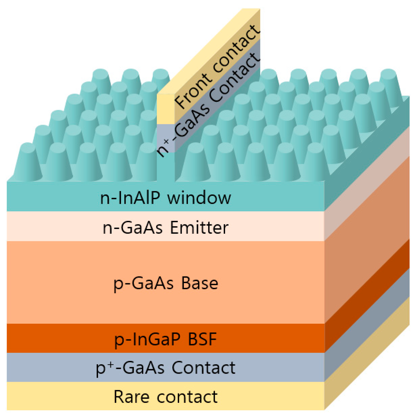
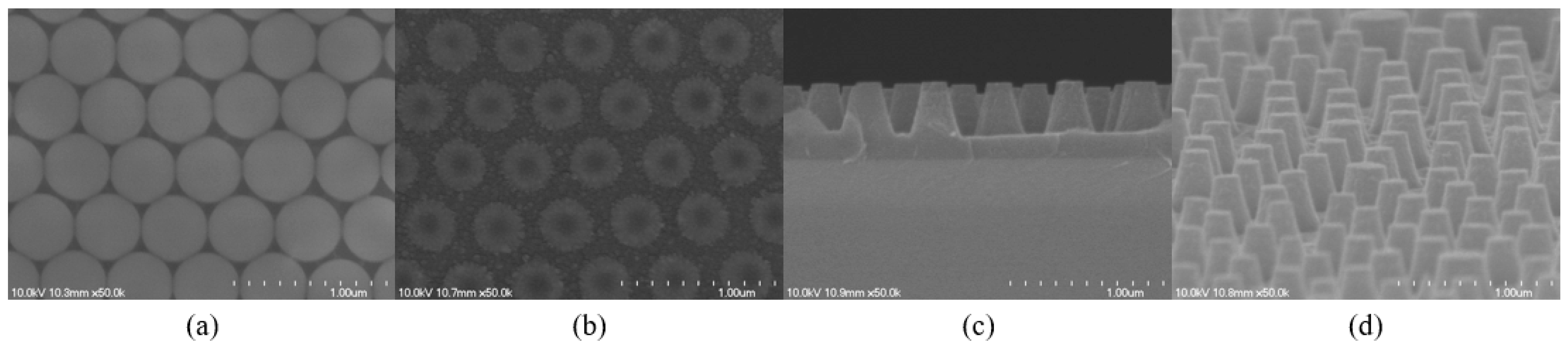
2. Materials and Methods

The inverted GaAs 1J SCs were grown on Si-doped (100) GaAs substrates oriented 2 °C off [111], through a metalorganic chemical vapor deposition (AIX200/4 RF, AIXTRON Inc., Cambridge, UK). Trimethylgallium, trimethylindium, and trimethylaluminum were employed as a group III source. Arsine and phosphine were employed as a group V source. Diethylzinc and disilane were employed as the p-dopant and n-dopant, respectively. The area of the fabricated SCs was 0.27 cm2. Commonly, the GaAs 1J SC was composed of a n+-GaAs Ohmic layer, n-InAlP window, n-GaAs emitter, p-pressure of 30 mTorr, and radio frequency power of 250 W for etching SiO2. The GaAs contact layer and InAlP window layer was etched using HBr and Ar gas by an inductive co GaAs base, and p-InGaP back surface field (BSF) layer as shown in Figure 1. The doping concentration and thickness of each layer were grown under the following conditions: a 0.3 μm p-type GaAs contact layer with a hole concentration of 1.49 × 1019 cm−3 and a GaAs bottom cell consisting of a 0.3 μm p-type GaAs contact layer with a hole concentration of 1.49 × 1019 cm−3, a 100 nm thick 3.94 × 1018 cm−3 p-type In0.51Ga0.49P back surface field (BSF) layer, a 3.3 μm thick 1.23 × 1017 cm−3 p-type GaAs base layer, a 100 nm thick 2.00E18 cm−3 n-type GaAs emitter layer, a 4.15E17 cm−3 n-type InAlP window layer, and a 0.3 μm thick 8.5 × 1019 cm−3 n+-type GaAs contact layer in succession. The doping concentrations of each layer were investigated by Hall measurement. The InAlP window layer with a thickness of ~500 nm was grown. Then, 150 nm of SiO2 was deposited on GaAs 1J SC by a plasma-enhanced chemical vapor deposition (PECVD) system (SLR-730, Oerlikon Corp., Freienbach, Switzerland). A monolayer of PS beads that floats on DI-water (diameter of ~400 nm, 4% w/v in DI-water, purchased from Thermo Fisher Scientific Corp., Waltham, MA, USA) was scooped by SiO2-deposited GaAs 1J SC and dried naturally. The diameter of dried PS beads was adjusted to ~300 nm by a reactive ion etching (RIE) system (FABstarRIE, Titiel Corp., London, UK) using O2 gas. The etched PS beads monolayer transferred the pattern to the SiO2 layer by etching SiO2 using CF4 gas by RIE, which is utilized as a mask layer. PS beads were eliminated by RIE using O2 gas after carrying out fabricating the SiO2 mask layer by RIE. RIE was operated at the working pressure of 60 mTorr and the radio frequency power of 80 W for etching PS beads and the working coupled plasma (ICP) system (SLR-770, Oerlikon Corp.). ICP was operated at the working pressure of 10 mTorr and the radio frequency power of 150 W for etching the GaAs/InAlP layer. The mask layer was removed by immersing SC in BOE for ~5 s. For exposing the NT InAlP window layer, the GaAs contact layer was etched by dipping in citric acid solution for ~60 s. The rough surface of NT InAlP layer was polished by dipping in the solution of HCl:H2O = 1:5 for 1 s. Then, 105 nm of SiNx was deposited on the polished NT InAlP widow layer as a passivation layer. The fabricated sequence of texturing is illustrated in Figure 2, and the schematic structure of GaAs 1J NT SC is shown in Figure 1.
In addition, in order to compare performances, two types of surface conditions of the GaAs 1J SCs were prepared with the ~30 nm of the InAlP window layer. One is an GaAs 1J SC with a bare surface, i.e., the InAlP window layer of the SC was exposed. The other one is the GaAs 1J SC with the planar 80 nm of SiNx as the ARC layer deposited by an ion beam-assisted deposition system (IBAD System, Infovion Inc., Richardson, TX, USA), which is a conventional anti-reflection method using a multi-layer, thin film, anti-reflection coating with various materials and thicknesses [13]. With the intention of investigating devices with different surface conditions, enlarged images of surfaces at high magnification were studied through a scanning electron microscope (SEM) (S-4700, Hitachi, Tokyo, Japan), the light reflectance was studied using the UV-VIS reflection measurement module (B0086703, Perkin Elmer Corp., Waltham, MA, USA), current density voltage (J-V) characteristics under 1 sun AM 1.5 G (100 mW/cm2) illuminance by the solar simulator (XIL-01B50KP, Technox Inc., Chicago, IL, USA), and EQE by the spectral response measuring system (S9230-MJ5, Soma Optics Ltd., Tokyo, Japan). Furthermore, η with various θs between the surface normal and the incident light beam from 0 °C to 70 °C at intervals of 10 °C were compared with different surface conditions so as to examine the omnidirectional effect. The distance between light source and optic acquisition of devices was kept constant while θ changed. All measurements were carried out at room temperature.

3. Results

The monolayer of naturally dried PS beads covered the planar surface as shown in Figure 3a. To make a SiO2 layer with a diameter of about 300 nm, PS beads were dry etched by RIE to have a suitable diameter. Figure 3b shows the shape in which the diameter of the 400 nm PS bead was changed to about 300 nm by RIE etching after carrying out fabricating the SiO2 mask layer by RIE. The GaAs contact layer and InAlP window layer were etched using HBr and Ar gas by ICP. Figure 3c,d shows the SEM cross-sectional image and 45 °C tilted surface of the NT InAlP window layer, respectively. The NT InAlP window layer was applied to the GaAs 1J SC.
Figure 4 shows the spectra of specular reflectance measured on GaAs substrates with different surface conditions: the bare GaAs surface, the planar ARC surface, and the three-dimensional NT InAlP surface. Both ARC and NT surfaces exhibited suppressed reflectance compared to the bare surface. The planar ARC layer suppressed the reflectance through destructive interference effects caused by out-of-phase reflected waves of the light from interfaces between the bilayers of ARC and SC. The NT layer reduced the reflectance by gradually changing the refractive index by the moth-eye effect [16,17]. The noticeable distinction of the plotted reflectance–λ curves between the ARC and NT surfaces is the difference of λ range, where the reflectance is effectively suppressed compared with the specular, reflected, bare GaAs surface. The NT surface suppressed the reflection at a wide λ range from 550 nm to 1200 nm evenly, which covers the whole range of GaAs 1J SCs enough. The suppressed reflectance by the NT surface mainly originates in the nanoscale three-dimensional layer. Since the geometric features of the factor NT surface exhibit the most index grading from air to the device, a remarkably low reflectance is achieved. Whereas the planar ARC surface suppresses the reflectance at a partial λ range, approximately from ~750 nm to ~1000 nm, and consequently reveals a limitation of the planar ARC layer. As a result, the broad λ range of reflectance is more considerably reduced by the NT surface than the planar ARC surface.
The effects of the surfaces with different conditions on the nanostructure are mostly smaller than the studied wavelengths; λ of the incident light regards the nanostructure as an effective medium, whose effective refractive index falls off the InAlP towards the bottom, significantly reducing the undesired reflectance through destructive interferences among the beams reflected from different depths into the nanostructure [17,19,22]. As the effective medium provides a graded refractive index between the air and InAlP because of the increased space filling, the photocurrent generation by each SC was examined from the EQE spectra, as shown in Figure 5. The EQE spectra reveal that both ARC and NT surfaces benefit the carrier generation of GaAs 1J SC and elongate the diffusion length [23]. However, there is no significant difference of the EQE spectra between the ARC and the NT SC as plotted in Figure 5, whereas the reflectance spectra between the ARC and NT surfaces, as shown in Figure 4, present a distinct difference.
Enhanced EQE affects current density (J) improvement, as in Equation (1):
E Q E = I / e P 0 / h c = J A / e P 0 / h c
where I is the current, e is the charge of one electron, P 0 is the total power of photons, h is the Planck constant, c is the speed of light, and A is the surface area of the device receiving the light. As a result, the improved J spectra of the ARC and NT SC compared to the bare surface SC was represented, as shown in Figure 6. The EQE of the ARC and NT SC increased similarly from the bare surface SC with no conspicuous offset between each other as shown in Figure 5; the J–V curves as plotted in Figure 6 reveal that the J of the ARC and NT SC increased with no conspicuous offset from the bare surface SC.
The specific measured device parameters from the J–V curves, as shown in Figure 6, are summarized in Table 1. In order to investigate the effect of the NT surface on GaAs 1J SC, the photovoltaic J–V characteristics were measured. As the bare surface SC for reference, the improved J was the main factor to increase η. As shown in Figure 4, the NT surface has a lower reflectance in a wider absorption wavelength range than that of the ARC surface, but the reflectance of the ARC surface is less in the wavelength band near the GaAs energy bandgap. As shown in Figure 5, the EQE of NT solar cells is greater than that of ARC solar cells, but the EQE of ARC solar cells is larger in the wavelength band near the GaAs energy bandgap. As a result of the reflectance and quantum efficiency, the current density of the NT solar cell is slightly lower than that of the ARC solar cell, but the open circuit voltage is slightly increased.
As shown in Figure 7, efficiencies were acquired with varying θ from 0 °C to 70 °C at intervals of 10 °C. The η of the NT SC is apparently higher than the η of the ARC SC at all ranges of θ. The η of the NT SC from 0 °C to 20 °C was almost preserved and the gaps of η between the NT and ARC SC were gradually wider from 50 °C to 70 °C. The η at 70 °C of the NT SC was about 3.2 times higher than the η of the ARC SC. It demonstrates that the NT surface alleviates the loss of η as θ increases compared to the planar ARC surface. Since the dimensions of nanotextures are increased in the bottom, the scattering effect becomes increasingly pronounced, and the incident photons are more likely to bounce back and forth among the NT surface. As a result, the optical path on the solar cell surface is prolonged, leading to enhanced absorption by the active region while θ is modified. Hence, the three-dimensional NT surface is distinguished from the planar ARC surface. It was found that NT SC has omnidirectionality.

4. Conclusions

In conclusion, the planar ARC and NT InAlP window SC increase the light harvesting more than the bare surface SC, which was found from the suppressed reflectance, enhanced EQE spectra, and JSC. In particular, the NT surface decreases the reflectance and effects across the broad λ range, containing the whole λ spectrum of the GaAs 1J SC. In addition, the NT SC was distinguished from the ARC SC by comparing the alleviated η loss of the NT SC with the η loss of the ARC SC as θ increased, which followed the purpose of this study to investigate the omnidirectionality of the NT surface on SCs. The presented concept and manufacturing technique are expected to benefit high-efficiency flexible SCs.

Author Contributions

Conceptualization, C.-W.K. and H.-J.K.; methodology of nanotexturing, C.-W.K. and H.-J.K.; fabricating the planar solar cell, G.-Y.P.; growing solar cells by MOCVD and H.-J.K.; calculation, J.-C.S.; investigation, C.-W.K.; writing—original draft preparation, C.-W.K.; writing—review and editing, H.-J.K.; supervision, H.-J.K.; funding acquisition, H.-J.K. All authors have read and agreed to the published version of the manuscript.

Funding

This research was supported by the Technology Development Program to Solve Climate Changes of the National Research Foundation (NRF) funded by the Ministry of Science ICT (2017M1A2A2048903), the Leading program of the National Research Foundation (NRF) funded by the Ministry of Science (2021M3H4A1A02051253), and Ministry of Trade, Industry and Energy (MOTIE) of the Republic of Korea (No. 70300026).

Institutional Review Board Statement

Not applicable.

Informed Consent Statement

Not applicable.

Conflicts of Interest

The authors declare no conflict of interest.

References

  1. Takamoto, T.; Yamaguchi, M.; Taylor, S.J.; Yang, M.-J.; Ikeda, E.; Kurita, H. Radiation resistance of high-efficiency InGaP/GaAs tandem solar cells. Sol. Energy Mater. Sol. Cells 1999, 58, 265–276. [Google Scholar] [CrossRef]
  2. Danilchenko, B.; Budnyk, A.; Shpinar, L.; Poplavskyy, D.; Zelensky, S.E.; Barnham, K.W.J.; Ekins-Daukes, N.J. 1 MeV electron irradiation influence on GaAs solar cell performance. Sol. Energy Mater. Sol. Cells 2008, 92, 1336–1340. [Google Scholar] [CrossRef]
  3. Yamaguchi, M. Radiation-resistant solar cells for space use. Sol. Energy Mater. Sol. Cells 2001, 68, 31–53. [Google Scholar] [CrossRef]
  4. Yamaguchi, M.; Okuda, T.; Taylor, S.J.; Takamoto, T. Superior radiation-resistant properties of InGaP/GaAs tandem solar cells. Appl. Phys. Lett. 1997, 70, 1566. [Google Scholar] [CrossRef]
  5. Dharmarasu, N.; Yamaguchi, M.; Khan, A. High-radiation-resistant InGaP, InGaAsP, and InGaAs solar cells for multijuction solar cells. Appl. Phys. Lett. 2001, 79, 2399. [Google Scholar] [CrossRef]
  6. Khan, A.; Marupaduga, S.; Anandakrishnan, S.S.; Alam, M. Radiation response analysis of wide-gap p-AlInGaP for superhigh-efficiency space photovoltaics. Appl. Phys. Lett. 2004, 85, 5218. [Google Scholar] [CrossRef]
  7. Schubert, M.B.; Werner, J.H. Flexible solar cells for clothing. Materials 2006, 9, 42–50. [Google Scholar] [CrossRef]
  8. Lee, Y.-H.; Kim, J.-S.; Noh, J.; Lee, I.; Kim, H.J.; Choi, S.; Seo, J.; Jeon, S.; Kim, T.-S.; Lee, J.-Y.; et al. Wearable textile battery rechargeable by solar energy. Nano Lett. 2013, 13, 5753–5761. [Google Scholar] [CrossRef] [PubMed]
  9. Wen, Z.; Yeh, M.; Guo, H.; Wang, J.; Zi, Y.; Xu, W.; Deng, J.; Zhu, L.; Wang, X.; Hu, C.; et al. Self-powered textile for wearable electronics by hybridizing fiber-shaped nanogenerators, solar cells, and supercapacitors. Sci. Adv. 2016, 2, e1600097. [Google Scholar] [CrossRef] [Green Version]
  10. Reb, L.K.; Bohmer, M.; Predeschly, B.; Grott, S.; Weindl, C.L.; Ivandekic, G.I.; Guo, R.; Dreibigacker, C.; Gernhauser, R.; Meyier, A.; et al. Perovskite and organic solar cells on a rocket flight. J. Joule 2020, 4, 1880–1892. [Google Scholar] [CrossRef]
  11. Kishi, Y.; Inoue, H.; Murata, K.; Tanaka, H.; Kouzuma, S.; Morizane, M.; Fukuda, Y.; Nishiwaki, H.; Nakano, K.; Takeoka, A.; et al. Ultralight flexible amorphous silicon solar cell and its application to an airplane. Sol. Energy Mater. 1991, 23, 312–318. [Google Scholar] [CrossRef]
  12. Dhere, M.G.; Ghongadi, S.R.; Pandit, M.B.; Jahagirdar, A.H.; Scheiman, D. CIGS2 thin-film solar cells on flexible foils for space power. Prog. Photovolt. 2002, 10, 407–416. [Google Scholar] [CrossRef] [Green Version]
  13. Zhao, J.; Green, M.A. Optimized antireflection coatings for high-efficiency silicon solar cells. IEEE Trans. Electron Devices 1991, 38, 1925–1934. [Google Scholar] [CrossRef]
  14. Yin, Y.; Li, Z.; Kuo, H.; Lu, T. Efficiency improvement of single-junction InGaP solar cells fabricated by a novel micro-hole array surface texture process. J. Semicond. Sci. Technol. 2009, 24, 085007. [Google Scholar]
  15. Yeh, L.; Tian, W.; Lai, K.; He, J. Exceptionally omnidirectional broadband light harvesting scheme for multi-junction concentrator solar cells achieved via ZnO nanoneedles. J. Sci. Rep. 2016, 6, 39134. [Google Scholar] [CrossRef] [Green Version]
  16. Boden, S.A.; Bagnall, D.M. Optimization of moth-eye antirefection schemes for silicon solar cells. Prog. Photovolt. Res. Appl. 2010, 18, 195–203. [Google Scholar] [CrossRef] [Green Version]
  17. Cai, J.; Qi, L. Recent advances in antirefective surfaces based on nanostructure arrays. Mater. Horiz. 2015, 2, 37–53. [Google Scholar] [CrossRef]
  18. Allred, D.D.; Larsen, Z.; Muhlestein, J.; Turley, R.S.; Willey, A. Effective medium theory, rough surfaces, and Moth’s eyes. J. Utah Acad. Sci. Arts Lett. 2009, 29, 273–286. [Google Scholar]
  19. Yeh, L.; Lai, K.; Lin, G.; Fu, P.; Chang, H.; Lin, C.; He, J. Giant efficiency enhancement of GaAs solar cells with graded antirefection layers based on syringelike ZnO nanorod arrays. Adv. Energy Mater. 2011, 1, 506–510. [Google Scholar] [CrossRef]
  20. Park, H.; Shin, D.; Kang, G.; Baek, S.; Kim, K.; Padilla, W.J. Broadband optical antirefection enhancement by integrating antirefective nanoislands with silicon nanoconical-frustum arrays. Adv. Mater. 2011, 23, 5796–5800. [Google Scholar] [CrossRef]
  21. Sahoo, K.C.; Lin, M.; Chang, E.; Lu, Y.; Chen, C.; Huang, J.; Chang, C. Fabrication of antirefective sub-wavelength structures on silicon nitride using nano cluster mask for solar cell application. Nanoscale Res. Lett. 2009, 4, 680. [Google Scholar] [CrossRef] [PubMed] [Green Version]
  22. Chao, Y.C.; Chen, C.; Lin, C.; Dai, Y.; He, J. Antireflection effect of ZnO nanorods arrays. J. Mater. Chem. 2011, 20, 8134–8138. [Google Scholar] [CrossRef]
  23. Photovoltaics Education. Available online: https://www.pveducation.org/pvcdrom/solar-cell-operation/quantum-efficiency (accessed on 5 December 2021).
Figure 1. Schematic structure of the NT InAlP window layer GaAs 1J SC.
Applsci 12 00601 g001
Figure 2. Schematic illustration of sequence of the nanotexturing process.
Applsci 12 00601 g002
Figure 3. SEM images: Top view of (a) PS beads monolayer on GaAs substrate and (b) PS beads, whose diameter of about 350 nm was adjusted by RIE using O2 gas, (c) a profile, and (d) tilted images of the NT InAlP window layer.
Applsci 12 00601 g003
Figure 4. Surface reflectance for the bare surface SC, SC with SiNx ARC, and InAlP NT surface.
Applsci 12 00601 g004
Figure 5. EQE for the bare surface SC, SC with SiNx ARC, and InAlP NT surface.
Applsci 12 00601 g005
Figure 6. J–V curves for the bare surface SC, SC with SiNx ARC, and InAlP NT surface.
Applsci 12 00601 g006
Figure 7. Efficiencies’ dependence on θ for the bare surface SC, SC with SiNx ARC, and InAlP NT surface.
Applsci 12 00601 g007
Table 1. Voc, Jsc, fill factor (FF), and η for J–V curves as shown in Figure 6.
VOC (V)JSC (mA/cm2)FFη (%)
Bare0.9121.500.7113.81
ARC0.9228.940.7219.07
NT0.9328.400.7419.44
Publisher’s Note: MDPI stays neutral with regard to jurisdictional claims in published maps and institutional affiliations.

