Article

Metrology for Measuring Bumps in a Protection Layer Based on Phase Shifting Fringe Projection

Center for Measurement Standards, Industrial Technology Research Institute, Bldg. 12, 321 Sec. 2, Kuang Fu Rd., Hsinchu 300, Taiwan
*
Author to whom correspondence should be addressed.
Appl. Sci. 2022, 12(2), 898; https://doi.org/10.3390/app12020898
Submission received: 26 November 2021 / Revised: 9 January 2022 / Accepted: 12 January 2022 / Published: 17 January 2022

Abstract

:
We developed a telecentric 3D measurement system based on the fringe projection technique to measure phases corresponding to the 3D shape of bumps on a surface. A measurement algorithm based on an area scan camera with a flexibly programmable region of interest (ROI) was applied to reconstruct the 3D model. Only the pixel information within the ROI is stored, which reduces the data volume and processing and accelerates the area scan acquisition. Experiments showed that the fringe projection system provided good linearity between the calibration and optical data with excellent accuracy. A reflectometry sensor was implemented to provide a correction offset to the bump height in a protection layer in a subsequent high-speed inspection.

1. Introduction

The development of optical 3D shape measurement methods is rapidly gaining importance in the manufacturing industry due to its capability of measuring and reconstructing real 3D moving objects [1,2,3,4]. Three-dimensional information about shaped objects on silicon wafers, printed circuit boards, or flat panel displays can be obtained in various ways that offer different tradeoffs between speed and resolution/accuracy. Triangulation is often used for the 3D reconstruction of production-worthy metrology [5,6,7]. The laser scanning and structured light methods are the two mainstream approaches based on the geometric triangulation principle for determining actual object shapes with high economic performance. In laser scanning, a laser line is projected onto a reference surface and the target object. The absolute positions of both lines on the imaging sensor plane are compared to provide 3D information on the object via a height map. The other widely used method is fringe projection, which encodes the depth information via the deformation of a known fringe pattern projection. Conventional applications have led to the conclusion that, when the same detector is employed for both methods, laser scanning offers superior throughput, while fringe projection has better displacement sensitivity [8].
Several studies have addressed improving the measurement speed and precision of the fringe projection technique to meet the full wafer inspection requirements of the advanced packaging industry [9,10,11]. The phase-shifting technique is based on using multiple projections of various stripe patterns to provide continuous phase maps and is the most well-known method for obtaining the absolute phase and corresponding object height. A three-step phase-shifting algorithm is the optimal choice because it requires the minimum number of fringe images for real-time 3D measurement. In most cases, three fringe patterns with a 120° phase shift to each other are sequentially projected onto the object by a projector, and an area camera is calibrated to grab fringe images of the object. Then, a phase map can be calculated from every three fringe images by phase-wrapping and unwrapping algorithms and is used to decode the 3D shape. Conventional phase shifting method was concerned by the issues of time consuming and limited frame rate. A three-row line scan camera has been tested in our previous system setup that was designed to simultaneously acquire three fringe images with a 120° phase shift in separate rows to achieve continuous scanning and high accuracy in real-time measurement. However, hardware system parameters including the fringe density, fringe projection angle, and magnifications of the projection lens and image collection lens all need to be accurately calculated and strictly adjusted to meet the requirements of the designed phase-shifting algorithm.
Three-dimensional imaging systems based on the fringe projection technique measure the absolute phase corresponding to the 3D shape of an object surface. To obtain the shape of the measured object, the absolute phase needs to be converted into depth data. When a small object is being measured, however, the distortion of an ordinary lens complicates the calibration. The inherently nonlinear and spatially variable relationship between the absolute phase of the projected fringe and the object surface depth is an issue for fringe projection technology involving high-accuracy metrology. Telecentric lens with the characteristics of low distortion, better magnification consistency and increased field depth has been proposed as a solution because the size of the object does not change with depth in telecentric imaging; thus, the absolute phase is linear with the depth, which simplifies the calibration process [12,13,14,15,16,17,18,19].
In recent years, the under bump metallurgy (UBM) layer used in conventional wafer-level chip scale packages (WLCSP) has been eliminated in favor of the UBM-free integration (UFI) fan-in WLCSP; this improves the bond between the solder ball and copper redirect pad and reduces the cost and package profile. However, measurement of the bump height has become more challenging with the deposition of a polymer protection layer (PL) in advanced WLCSP processes. The PL, which is usually polyimide (PI) or polybenzoxazole (PBO) is used to secure the solder in place; it is semitransparent and varies in thickness, which introduces errors in measurements of the bump height with the triangulation technique [20]. Current manufacturers have worked around this problem by applying a light interferometer profiler to provide a bump height offset value to the triangulation measurement. The PL thickness is assumed to be obtained by measurement through the film to the substrate. However, when there is more than one semitransparent layer (e.g., an oxide insulation layer between the top PL and bottom silicon substrate), this makes the interference image contrast returned by the interferometric measurements ambiguous along the layer depth. The reflection of the Si substrate has an especially strong influence. Because protection layers are typically a few to tens of microns thick, a vertical scan along a given range is time consuming; this makes it impossible to complete a 100% inspection in time, which limits the accuracy and repeatability of the bump height measurement.
This paper presents a major effort towards improving the performance of 3D shape measurement systems based on fringe projection and phase shifting. A novel measurement algorithm was developed that is based on an area scan camera with a flexibly programmable region of interest (ROI) sensor area containing selectable rows to simultaneously acquire three fringe images with 120° phase shifts. Because only the pixel information within the ROI is stored in the memory, this tremendously reduces the data volume and processing and greatly accelerates the area scan acquisition. Sufficient information is retained to reconstruct a 3D model in a continuous scan mode instead of the conventional approach of taking three full-field fringe images sequentially in pause mode; this improves the measurement frame rate up to several hundredfold. In addition, the hardware system can be flexibly adjusted compared with the previous three-row line scan camera as long as the ROI contains the signal of the three rows with 120° phase shifting. A reflectometry sensor is implemented for measuring the onsite PL thickness to simultaneously and accurately provide the proper calibration map for measuring the bump height at each site. A spectroscopic reflection model and Fourier transform (FT) analysis algorithm, which are applicable in the case of a silicon substrate covered by a thick semitransparent PI layer on top of another semitransparent insulating film, were developed to accurately determine the thickness of each transparent film and their contributions to the bump height measurement error. Eliminating the strong reflection effect of the silicon substrate in optical measurements is not easy; spectroscopic reflection model fitting may be the best way to clearly identify the multiple interfaces between the air and silicon substrate.

2. Fringe Projection System and Sample Details
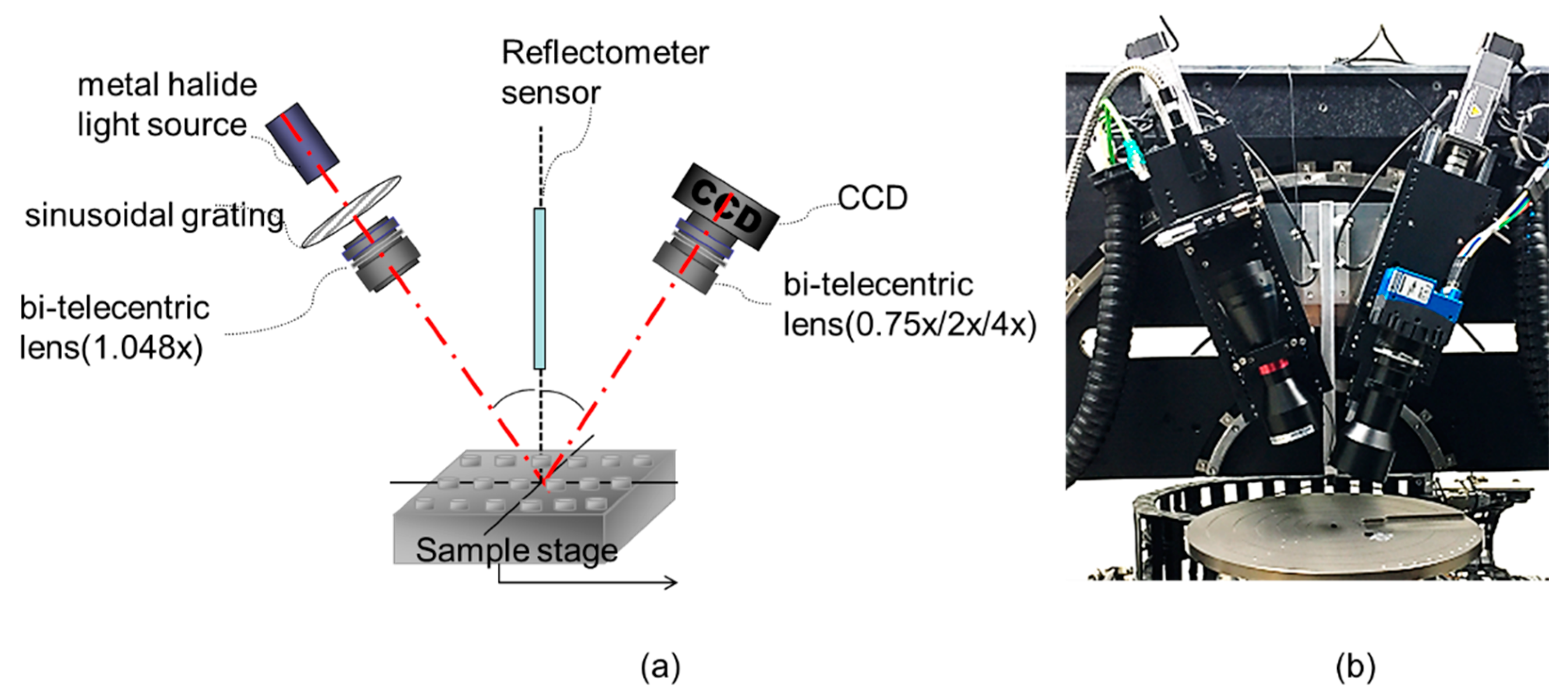
2.1. System Setup

We used telecentric objective lenses for both illumination and detection. Telecentric lenses create images of the same size at different distances within the field depth. The fringe projection module and image detection unit are mounted on a guide so that the projecting and detection angles can be adjusted for various applications. For most wafer-level substrate applications, the specular mode is adopted: the fringe incident angle is the same as the image collection angle so that the strongest reflective signal can be acquired. For other substrates such as a printed circuit board, the image unit is moved to the vertically mounted position so that as much of the scattered signal can be captured as possible. A sinusoidal grating with a grating direction parallel to the line of the light source is placed at the back focal point of the telecentric lens. The area scan camera sensor transfers pixel data from one row of detectors to the next in synchronization with the motion of the sample stage.

2.2. System Design

Figure 1 shows the telecentric 3D measurement system. It has three parts: the optical imaging system, projection system, and object space. The optical imaging system consists of a telecentric lens (Net-Gmbh L-VS-LTC series) with a selectable magnification (0.75×, 2×, or 4×) and a high-speed area scan camera (Mikrotron EoSens 12CXP+) with a resolution of 4096 (H) × 3072 (V) pixels and image field having a diagonal of 32.6 mm. The camera pixel size is 4.5 μm × 4.5 μm, which corresponding to the lateral sampling for the selectable magnification 0.75×, 2×, and 4× are 6 μm, 2.25 μm, and 1.13 μm respectively. The camera can be set to a smaller ROI so that only the pixel information within the ROI is stored in the memory, and the frame rate can be up to 10,100 fps with an active sensing area of 4096 (H) × 50 (V) pixel. The measuring speed is determined by the frame rate multiplied by the lateral sampling, which can be up to 60 mm/s (0.75×), 22.5 mm/s (2×), and 11.25 mm/s (4×) respectively. The projection system comprises a telecentric lens (ES Telecentric Lens ESCM35F-42-AL/1.048×) and 250 W metal halide light source with lightline lenses (A08806 aperture lenses dimension 3″). The projection system can project a sinusoidal fringe, and each bright stripe is parallel. Sinusoidal gratings with 4, 5, or 8 lines/mm density can be selected to flexibly and optimally introduce the phase-shifting algorithm into the bump measurement for wide ranges of heights and pitches. The object is placed on a high-precision stage with both x and y axial movement range of 300 mm.
A normal incidence reflectometer sensor was implemented on top of the sample to measure the PL thickness. The spectrum is measured in the broadband wavelength range of 375–780 nm. The normal incidence measurement largely relies on the interference between light scattered from different locations on the target structure. The reflectance spectrum typically has regular oscillations over a large wavelength range. The limiting factor in this case is the pixel resolution of the charge-coupled device (CCD) detector, which is about 0.4 nm at the upper wavelength limit of 780 nm.

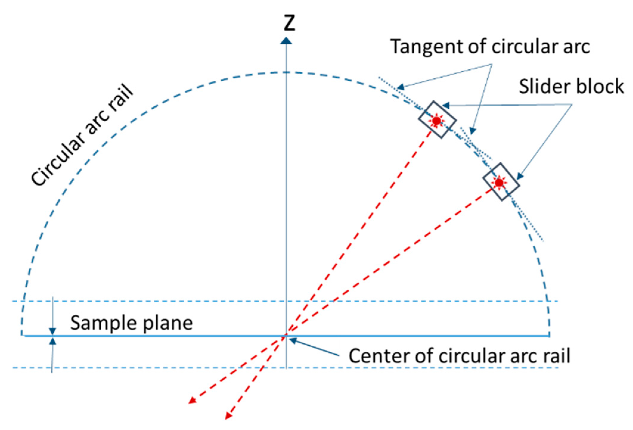
2.3. Reference Plane Identification and Rotation Center Calibration

To ensure that the sample is placed at the optimal focus position, the sample platform needs to be adjustable perpendicular to the z-axis and contain the center point of the circular arc rail. Two laser point sources are mounted separately on the slider blocks, which can individually move on the same circular-arc rail. Both point toward the center of the circular motion orbit, as shown in Figure 2. Consider two virtual lines along the laser light that are perpendicular to the tangent of the circular arc; their intersection reveals the center point of the circular arc rail. The sample plane can be slightly adjusted up and down to reach the best focus position that minimizes the merged laser spots.

2.4. Sample Details

Three of the test samples are introduced here and the measurement results will be shown later in Section 4 and Section 5.
A calibrated transfer standard with nine nominal step heights of 5, 15, 25, 35, 45, 55, 65, 75, and 85 µm was measured with a traceable stylus instrument and used to evaluate the performance of the fringe projection system at measuring the bump height.
A ball grid array (BGA) sample with a unit size of 6 mm × 6 mm. The diameter of the double peripheral solder bumps was around 100 µm, and the height was around 25 µm. The pitch of the bump array was 200 µm.
A surface-mounted device (SMD)-type BGA sample in the PL layer with a unit size of 5 mm × 5 mm. The diameter of the Sn bumps was around 200 µm, and the height was around 165 µm. The pitch of the bump array was 400 µm.

3. Theoretical Model of Fringe Projection Profilometry

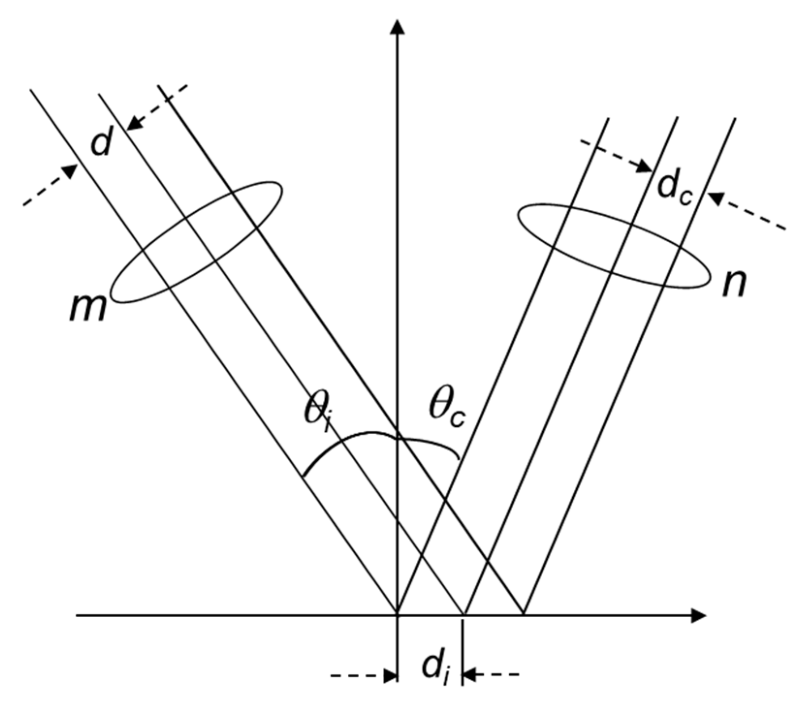
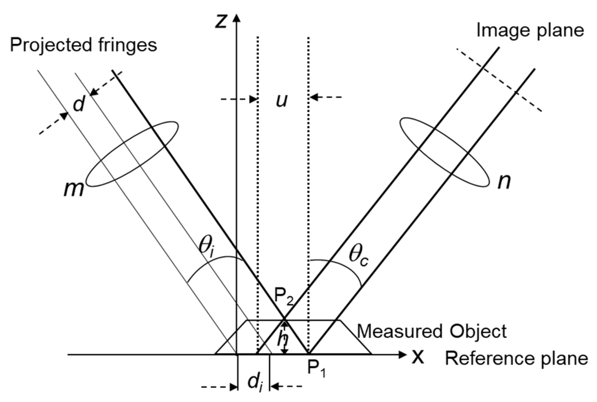
3.1. Basic Theoretical Model for Fringe Projection Profilometry

Figure 3 shows the sinusoidal fringe patterns when projected at an angle of θi onto a sample surface. The diffracted light is collected over the angle θc, and the sinusoidal grating pitch is d. The grating pitch di projected along the telecentric lens onto the sample plane is given by
d i = d m × cos θ i
where m is the magnification of the bi-telecentric lens of the projection module. The grating pitch dc acquired on the CCD camera plane is given by
d c = d m × cos θ i × n cos θ c
where n is the magnification of the bi-telecentric lens of the imaging module.

3.2. Three-Step Phase-Shifting Technique

The projected sinusoidal fringe pattern intensity I(x, y) on the camera plane for every pixel (x, y) can be described as follows:
I ( x , y ) = I 0 ( x , y ) + I ( x , y ) cos ϕ ( x , y )
where I 0 (x, y) is the background intensity proportional to the object reflectance and illumination intensity and I (x, y) is the fringe contrast. To determine the phase value φ(x, y), we simply use the three-step phase-shifting algorithm. Three corresponding rows of pixels within the ROI for which the linear direction is parallel to the fringes takes the following forms of images:
I 1 ( x , y ) = I 0 ( x , y ) + I ( x , y ) cos ϕ ( x , y ) I 2 ( x , y ) = I 0 ( x , y ) + I ( x , y ) cos ( ϕ ( x , y ) + 2 π / 3 ) I 3 ( x , y ) = I 0 ( x , y ) + I ( x , y ) cos ( ϕ ( x , y ) + 4 π / 3 )
By solving the above equations, we can find the phase at each pixel point:
ϕ ( x , y ) = tan 1 [ 3 I 1 I 3 2 I 2 I 1 I 3 ]
The average background intensity I 0 (x, y) and fringe contrast I (x, y) respectively given by
I 0 ( x , y ) = I 1 + I 3 + I 2 3
I ( x , y ) = 3 ( 2 I 1 I 3 ) 2 + ( 2 I 1 I 2 I 3 ) 2 3

3.3. Phase-Height Conversion

In order to introduce the three-step phase-shifting image into the camera, the ratio of dD/dc is 1/3:
d D = 1 3 d c = 1 3 d i × n cos θ c
where dD is the selected pixel row spacing (from center to center) within the camera ROI, which corresponds to one-third of a collecting fringe pitch. Thus, the three selected rows with equal spacing dD within ROI can simultaneously acquire three fringe images with 120° phase shifts. A fringe originally positioned at P1 is displaced to P2 when a curved profile is measured, as shown in Figure 4. To simplify the derivation, we considered the problem as one-dimensional, where the same result holds for both the x and y axes. The displacement caused by the shift in the fringe position can be given by
u ( x ) = h ( x ) ( tan θ i + tan θ c )
where h is the height of P2 above the reference plane. This gives the modulation factor M(x):
M ( x ) = u ( x ) d i = h ( x ) ( tan θ i + tan θ c ) d m cos θ i = m × h ( x ) d sin ( θ i + θ c ) cos θ c
The phase value φ(x, y) acquired in the image plane is given by
ϕ ( x ) = u ( x ) d i × 2 π = 2 π × m × h ( x ) d sin ( θ i + θ c ) cos θ c
Thus, the height-to-phase conversion equation gives
h ( x ) = d 2 π m cos θ c sin ( θ i + θ c ) ϕ ( x )

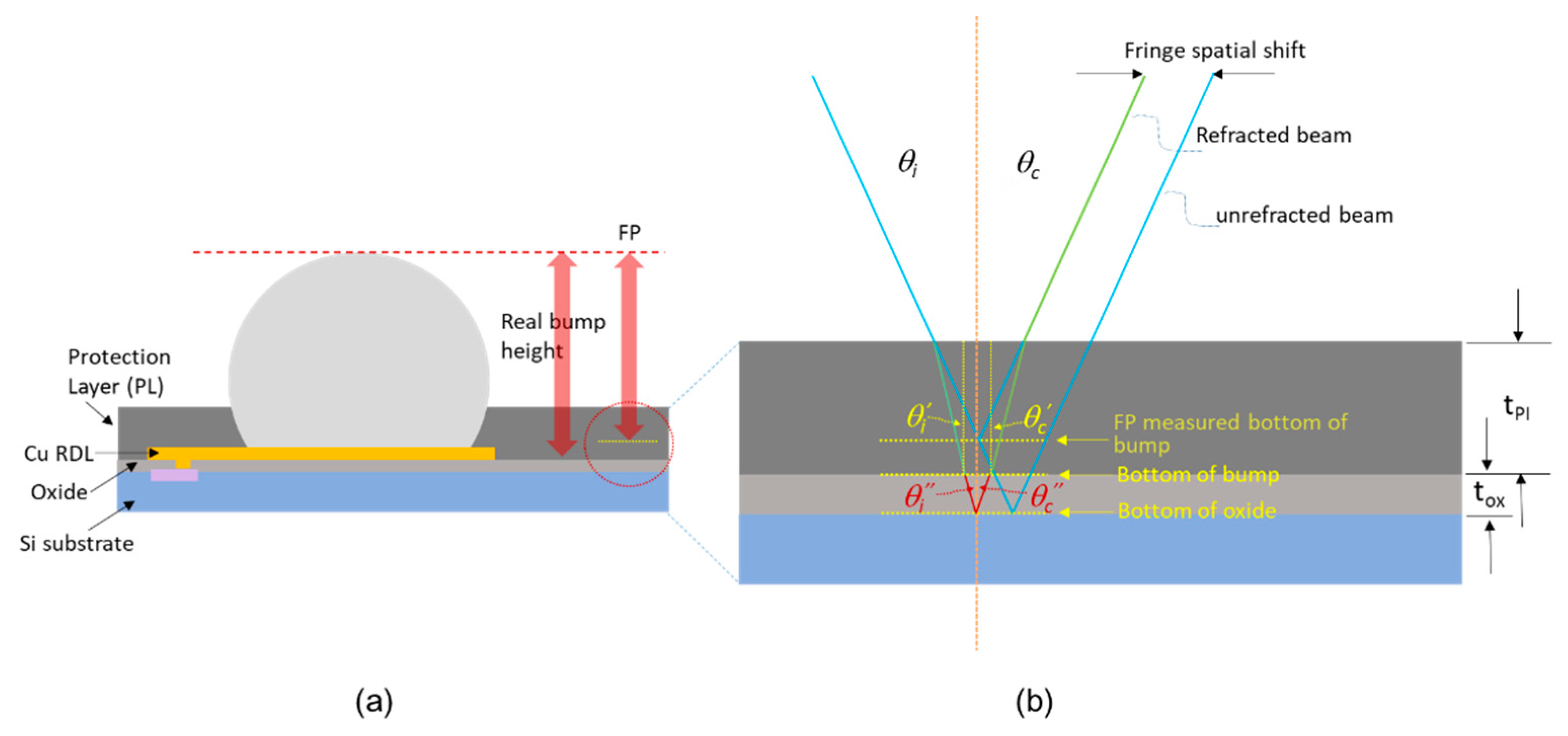
3.4. Bump Height Correction in Polymer Layers

A PL is used in an UFI fan-in WLCSP to help secure the solder pumps in position, as shown in Figure 5a. The solder balls are directly mounted on the Cu redistribution layer (RDL), which routes electrical signals from the original pads of the chip to the desired area array pads. When the triangulation method attempts to detect the bottom of the PL (blue line assumed), which has a semitransparent medium and larger index of refraction, the transmitted and reflected light from the bottom of the PL (green line) captured by the camera creates a lateral fringe shift that causes a perceived height recession in the calculation, as shown in Figure 5b. The PL thickness varies across the wafer, which introduces varying errors in the measured bump height from site to site. Thus, the in situ thickness of the PL layer needs to be considered to provide an accurate bump height correction for precise 3D measurement.
In order to quantitatively analyze the influence of the PL optical properties on the measurement accuracy, we considered a new approach where a reflectometric sensor is used to accurately measure the PL thickness at representative locations across the wafer, and the bump height offset to apply to fringe projection measurements is simultaneously calculated. The reflectometric sensor is capable of nanometer-scale accuracy and repeatability; in particular, its sensing time within 10 ms at each sampling site is fast enough to provide the correct offset as a function of the PL thickness.
The fringe refraction inside the PL layer is based on Snell’s law:
sin θ i = n P L sin θ i ; n P L sin θ c = sin θ c
where n P L is the refraction index property of the PL and θ i and θ c are the refracted projection and collection angles, respectively. Because we used a specular setup where the incident projection angle θ i is equal to the collecting angle θ c , the fringe displacement u P L in the lateral direction due to traveling around the PL layer is given by
u P L ( x ) = t P L ( x ) ( tan θ i + tan θ i ) = 2 t P L ( x ) sin θ i n P L 2 sin 2 θ i
where t P L (x, y) is the thickness of the PL at the representative location (x, y) across the wafer. The offset of the phase value Δφ(x,y) due to PL refraction acquired in the image plane is given by
Δ ϕ ( x ) = 2 π d i × 2 t P L ( x ) × ( tan θ i tan θ i ) = 2 π d i × 2 t P L ( x ) × ( tan θ i sin θ i n P L 2 sin 2 θ i )
When combined with Equation (12), the corrected bump height to phase conversion equation is given by
h ( x ) = d 2 π m cos θ c sin ( θ i + θ c ) [ ϕ ( x ) + Δ ϕ ( x ) ]
The real bump height is defined as from the bottom of the PL to the top of the bump instead of only the bump height above the PL. Because of the thickness variation of the PL across the wafer, the PL thickness should be considered in the bump height measurement to improve the accuracy of the coplanarity measurement.

4. Measurement Algorithm and System Calibration

A reference standard with calibrated heights was used to evaluate the performance of our fringe projection system at measuring various bump heights. The transfer standard containing nine nominal step heights of 5–85 µm was investigated with a traceable stylus tool according to ISO 5436-1. The average data from a series of tractile measurements on each step height were taken as the certified step heights, as listed in Table 1.
Figure 6a shows the measurement results with the fringe projection system. The images were acquired using the telecentric lens with magnification of 2× and the corresponding lateral sampling of 2.25 μm here. Figure 6b shows the comparisons between the calibrated heights and the optical measurement data, which has a good linearity fit of 0.99 and a small systematic offset of 0.44 µm along the extrapolation. The large range of measurements (5–85 µm) led to a discrepancy of <3.4%: <0.99 µm for the step height range listed in Table 1.

5. Experimental Results and Discussion

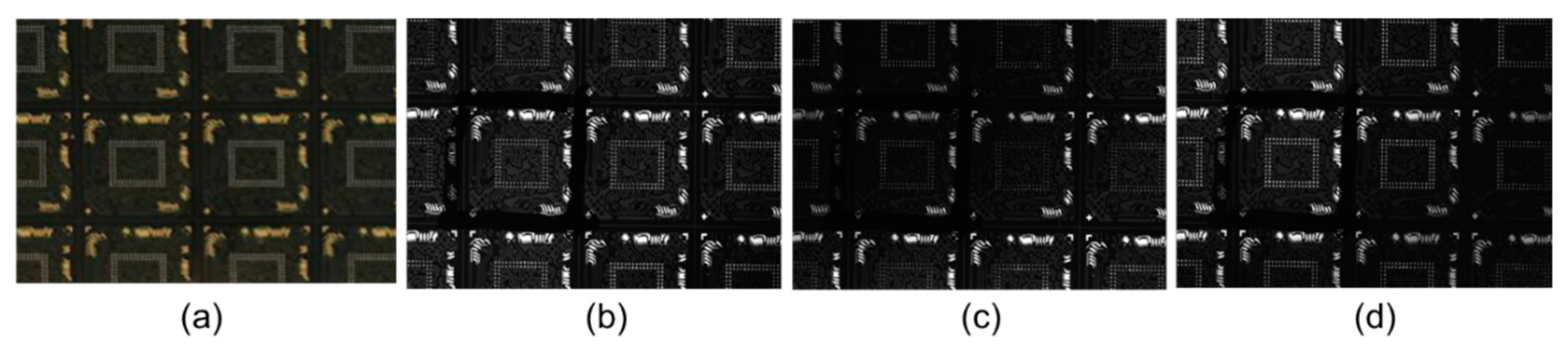
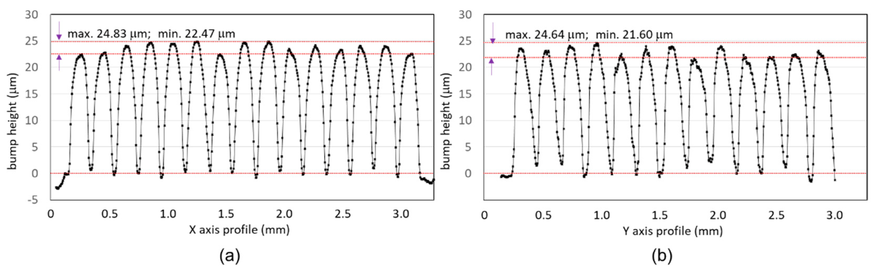
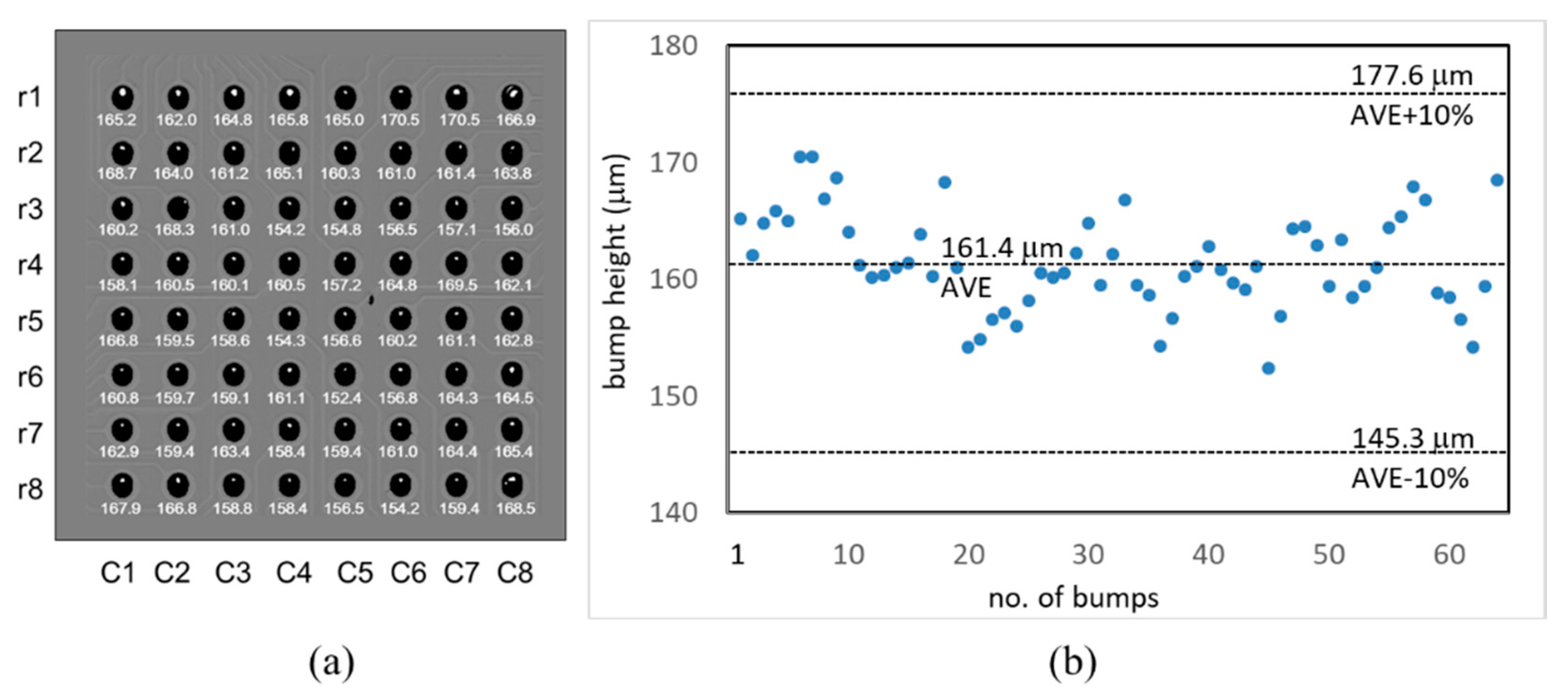
5.1. Measurement of Double Peripheral Solder Bumps

A BGA sample of 6 mm × 6 mm size containing double peripheral solder bumps was measured. With samples of the size of 6 mm × 6 mm, more than two sets of matrix arrays can be viewed along the scanning direction. The measurement process can be adjusted and performed fully automatically. The single exposure time to acquire the image data is 70 μs. By coping with the selected ROI sensor area of 4096(H) × 50(V), sufficient information of three fringe images with 120° phase shifts are retained to reconstruct a 3D model in a continuous scan mode. Figure 7 shows the result for the BGA sample measurements. Figure 7a shows a photo of the measurement area. Figure 7b–d shows three acquired images with a 120° phase shift. The algorithm with three-step phase-shifting algorithm was then applied to compute the phase map of the scan area, as indicated within the red frame area in Figure 8a. The wrapped phase map calculated by Equation (5) and the 3D reconstructed topography that was converted from the wrapped phase map are shown in Figure 8b,c respectively. It is possible to take profiles in any direction from the 3D measurement. For example, the red lines in Figure 8b denote the measurement data along the x and y axes used for the bump height calculation. A Gaussian filter with (5 × 5) radius was used to smooth the random noise.
Figure 9 shows the bump height calculation results along the red lines shown in the 2D phase map of Figure 8b. Figure 9a,b show the distribution of bump heights along the x and y axes, respectively. The bump heights were calculated by taking the difference between each bump’s peak and valley. The average bump heights were 23.65 and 23.12 µm along the x and y axes, direction respectively.
The algorithm for determining the bump heights is similar to that for characterizing the step heights, which subtracts the average height of the bottom area from the height of the top of each bump. In a repeatability test, measurements taken 30 times showed a standard deviation of less than 0.40 µm (1σ). Thus, the repeatability deviation was about 50 times less than the designed bump height.

5.2. Height Measurement of Bumps in a Polymer

An SMD-type BGA sample in the PL layer with a unit size of 5 mm × 5 mm was investigated.

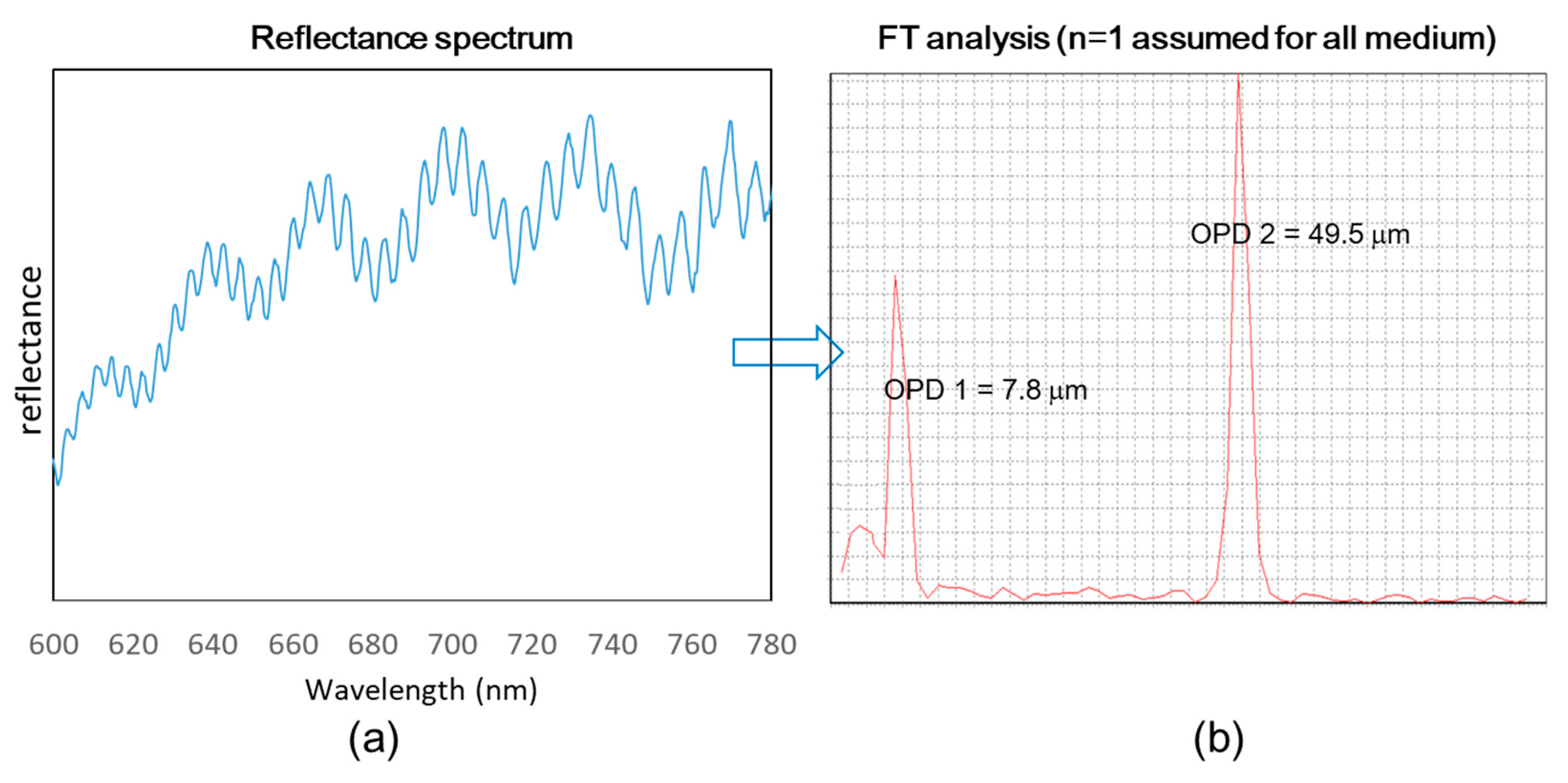
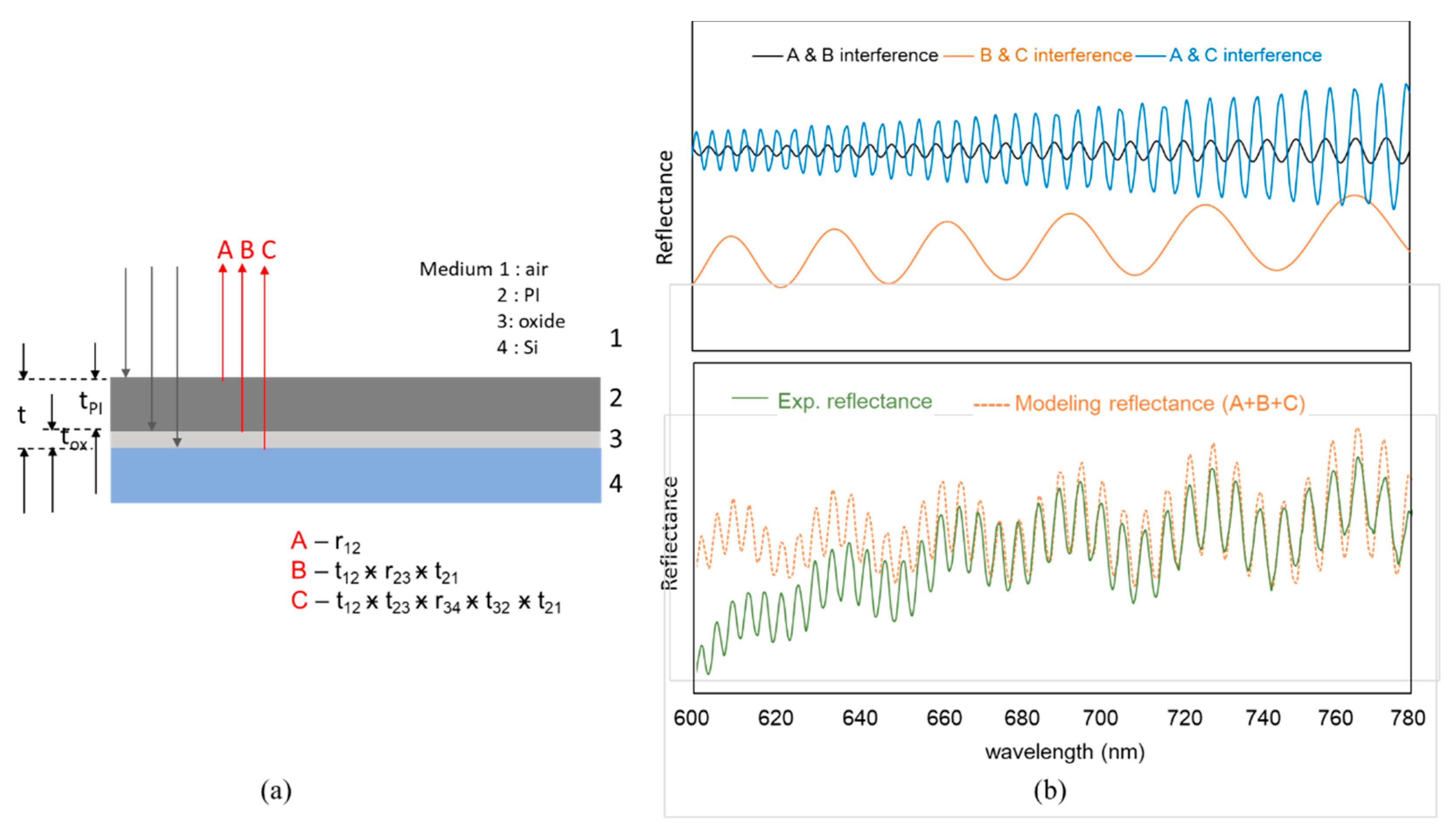
5.2.1. Reflectrometric Spectrum Model Fit

Figure 10a shows a reflectrometric spectrum for the measured PL on the BGA sample. The illumination area on the sample surface was around 13 µm, which was at nearly the center of the fringe projection position. Two distinct frequencies of oscillations were observed, which indicated more than one layer on top of the substrate. We used Fourier transform (FT) analysis to calculate the optical path difference (OPD) along the top surface to the bottom substrate, as shown in Figure 10b. The frequencies for the two-layer thickness were well separated from each other. OPD 1 and OPD 2 needed to be divided by the layer medium’s refractive index to obtain the geometric thickness. Figure 11a shows the simulation model for this case, in which a silicon substrate had an insulating oxide layer with the thickness t o x above and a PI layer with a thickness t P I on the top. The three reflected light waves (A, B, and C) could interfere with each other. The reflecting media 1–4 were defined as air, PI, oxide, and silicon, respectively. The refractive indices were constants for air, PI, and oxide at 1, 1.653, 1.47, respectively, and varied with the wavelength for silicon: 6.706 at 375 nm and 3.696 at 780 nm. According to the Fresnel equation, light path A in air reflects off the top of the PI layer to shift 180°, and its electrical field reflectance is multiplied by the reflecting factor r 12 [21]. Light path B off the oxide surface is transmitted through the PI layer and undergoes the phase shift e 2 π n P I t P I λ ; its electrical field reflectance is multiplied by the transmitting factor t 12 (transmission from air into PI), reflecting factor r 21 (reflection from oxide in the PI medium), and transmitting factor t 21 (transmission from PI to air). Light path C off the silicon surface shifts 180° and transmits through the oxide film and PI layer to undergo the phase shift e 2 π n P I t P I λ × e 2 π n o x t o x λ ; its electrical field reflectance is multiplied by the transmitting factor t 12 (transmission from air to PI), transmitting factor t 23 (transmission from PI to oxide), reflecting factor r 34 (reflection from silicon surface in the oxide medium), transmitting factor t 32 (transmission from oxide to PI), and transmitting factor t 21 (transmission from PI into air). The combined reflectance spectrum can be calculated by adding the interference spectrum of each pair of reflecting light paths A–C, as shown in Figure 11b. Because the oxide–silicon surface acts like a mirror, a stronger signal at the corresponding OPD 2 (A and C interference) can be acquired compared to the detection of the light reflected by the interface between the oxide film and PI layer (A and B interference). The amplitude of the interference A and B is too weak and has ignorable contribution to the total reflectance spectrum. A modulation signal at the corresponding OPD 1 comes from the light bouncing from the oxide film with the light reflected from the silicon substrate. Thus, the DFT results for OPD 1 and OPD 2 in Figure 10b correspond to t o x and ( t P I + t o x ), respectively. The optical thickness of the oxide film is given by OPD 1 =   n o x (λ) × t o x which was 7.8 µm (= 1.47 × 5.31 µm). The optical thickness of the additional PI and oxide film is given by OPD 2 = n P L (λ) × t P I + n o x (λ) × t o x , which was 49.5 µm (= 1.653 × 25.34 + 1.47 × 5.31 µm). In addition to the film thickness and optical constants, other properties such as the roughness of the PI–oxide and oxide–silicon interface also influenced the amplitude of the reflectance, especially at shorter wavelengths. Thus, the reflectance spectrum in the range of 600–780 µm was selected for the comparison [22].

5.2.2. Comparison of PL Measurement with Scanning White Light Interferometry

We used a Mirau-type scanning white light interferometer (SWLI) to verify the thickness of the semitransparent films measured by the reflectometer as described in Section 5.2.1 and shown in Figure 12a. The SWLI system translated vertically so that the surfaces of the upper and lower films passed through the focus. For each location in the field of view, two sets of interference fringes developed during the scan: one corresponding to the best focus at the air–PI interface and the other corresponding to the oxide–Si substrate interface. First, the vertical centers of the two fringe envelopes were determined. Then, the distance (OPD) between their centers was calculated, as shown in Figure 12b. The intensity corresponding to the PI–oxide interface was too weak to be seen; thus, the fringe envelop method applied in SWLI could not be used to accurately determine the PL layer thickness.

5.2.3. Bump Height Correction for Polymer Layers

Figure 13a,b show modified versions of Figure 5a,b, respectively, with an additional oxide layer between the PI and Si substrate based on the reflectance spectrum presented in Section 5.2.1. When the fringe projection method was used to detect the bottom of PI, the transmitted and reflected light passing through the PI (green line assumed) and oxide (red line assumed) and captured by the camera both created lateral fringe shifts that caused perceived height recessions in the calculation. Equations (13)–(16) were modified to Equations (17)–(20) to eliminate the influence of the PI and oxide on the bump height measurement. The fringe refraction inside the PI and oxide layer is based on Snell’s law:
sin θ i = n P L sin θ i = n o x sin θ i ; n o x sin θ c = n P L sin θ c = sin θ c
where n P L and n o x are the refraction index properties of PI and oxide, respectively, and the refracted angles of projection and collection in the PI and oxide layers are θ i , θ c and θ i , θ c , respectively. Because we used the specular setup, where the incident projection angles θ i and θ i are equal to the collection angles θ c and, θ c , the fringe displacements u P L and u o x in the lateral direction due to traveling around the PI and oxide layers are given by
u P L ( x ) = t P L ( x ) ( tan θ i + tan θ c ) = 2 t P L ( x ) sin θ i n P L 2 sin 2 θ i
u o x ( x ) = t o x ( x ) ( tan θ i + tan θ c ) = 2 t o x ( x ) sin θ i n o x 2 sin 2 θ i
where t P L (x) and t o x (x) are the thicknesses of PI and oxide, respectively, at the representative location x across the wafer. The offsets of the phase value Δ ϕ P L (x) and Δ ϕ o x (x) due to PI and oxide refraction were acquired in the image plane:
Δ ϕ P L ( x ) = 2 π d i × 2 t P L ( x ) × ( tan θ i tan θ i ) = 2 π d i × 2 t P L ( x ) × ( tan θ i sin θ i n P L 2 sin 2 θ i )
Δ ϕ o x ( x ) = 2 π d i × 2 t o x ( x ) × ( tan θ i tan θ i ) = 2 π d i × 2 t o x ( x ) × ( tan θ i sin θ i n o x 2 sin 2 θ i )
When combined with Equation (16), the corrected bump height to phase conversion is given by
h ( x ) = d 2 π m cos θ c sin ( θ i + θ c ) [ ϕ ( x ) + Δ ϕ P L ( x ) + Δ ϕ o x ( x ) ] t o x ( x )
The BGA bump array in the PI sample as shown in Figure 14a was analyzed in detail here. According to Equation (22), θ i = θ c θc = 19.6°, d = 250 µm, m = 1.048×, and the conversion factor d 2 π m cos θ c sin ( θ i + θ c ) has a constant value of 56.6. The phase modification terms Δ ϕ P L and Δ ϕ o x in Equations (20) and (21) are given by
Δ ϕ P L ( x ) = 0.0074 × t P L ( x ) ;   Δ ϕ o x ( x ) = 0.0060 × t o x ( x )
Equation (22) can be expressed as
h ( x ) = 56.6 × ϕ ( x ) + 0.42 × t P L ( x ) 0.66 × t o x ( x )
As an example, we took a PI thickness t P L of 25.34 µm and oxide thickness t o x of 5.31 µm. The height correction terms from Δ ϕ P L and Δ ϕ o x were +10.64 µm and −3.50 µm, respectively, which formed a +7.14 µm correction value when added to the fringe projection measurement results. Because the variations in the PI and oxide thickness within the test die were less than 0.74 and 0.19 µm, respectively, the fluctuations in the bump height correction value were around 0.3 and 0.13 µm, respectively. Figure 14a shows the unwrapped phase map of the 8 × 8 bump array on the polymer structure and the bump height map when corrected for the influence of the PI and oxide thicknesses. Figure 14b shows the corrected fringe projection measurements of the bump height varied from 152.4 µm to 170.5 µm with a coplanarity of 5.5% for all bumps on the 8 × 8 BGA array.

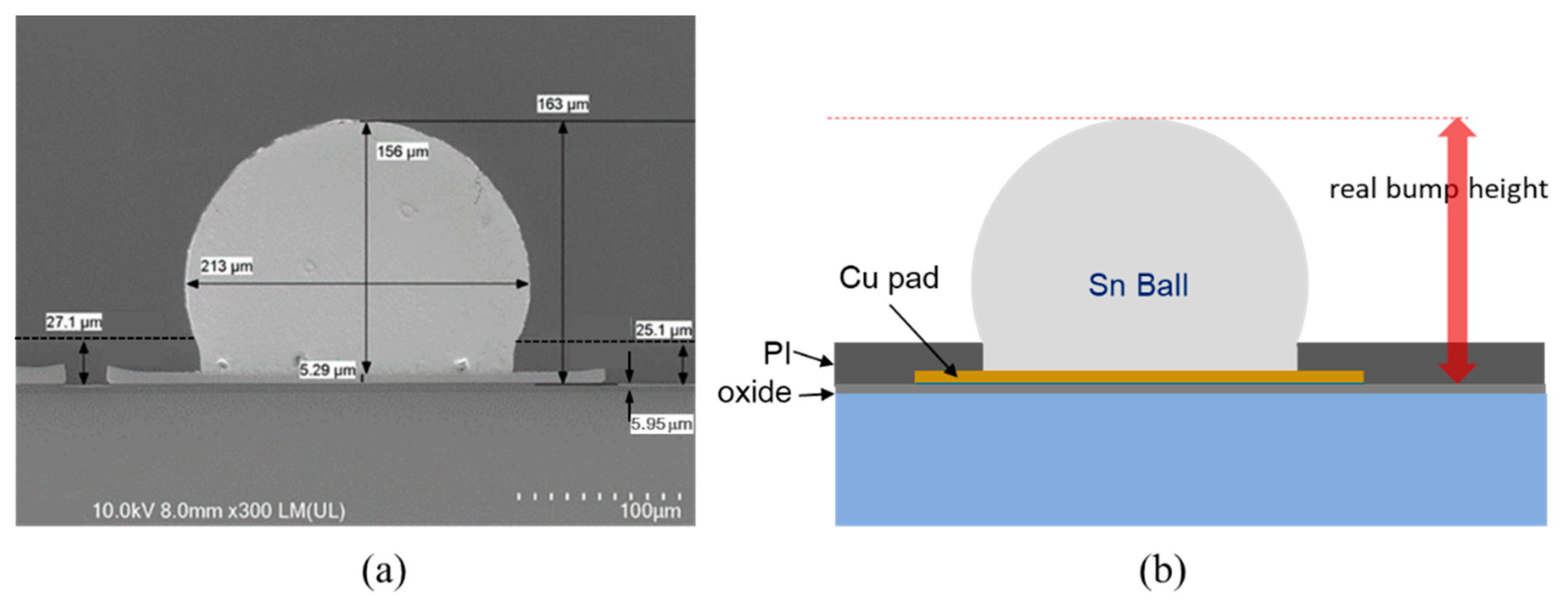
5.2.4. Comparison of 3D Measurement with Scanning Electron Microscopy

Figure 15a shows the cross-section SEM results for the bump on the PI sample presented in Figure 14a. The bump height was 163 µm, the PI thickness was 25.1 µm on the right side to 27.1 µm on the left side, and the oxide layer thickness was 5.95 µm. Figure 15b shows a schematic labeling the material in Figure 15a. The cross-sectional SEM was only performed for a single measurement cut made at one site owing to limitations of time and expense. The location of the cut SEM sample was inside the BGA array measured by the fringe projection and reflectometer, but we could not exactly identify which bump. This was good as an independent method for verifying the bump height but it is not a convenient and nondestructive method for analyzing the bump height or coplanarity as required for global measurement of the full site.

6. Conclusions

This paper presents a novel designed module that works with an improved frame rate and is easily compatible with the hardware system by adjusting the ROI. We explored a measurement algorithm solution for eliminating the effects of PI or other material layers on top of the surface, which can influence the measurement accuracy of bump heights/coplanarity. The spectroscopic reflection model and FT analysis method clearly identified the air–PI layer, PI layer–oxide, and oxide film–silicon substrate interfaces; they are useful for accurately determining the thickness of each layer and eliminating their influence on the bump height measurement accuracy.
Future work will involve the stage system integration combining a planar XY table with a 300 mm × 300 mm travel range and a rotational stage with 360° angle adjustment range. A fringe projecting module with a selectable fringe density and adjustable projecting angles will be tested to flexibly and optimally introduce the phase-shifting algorithm to bump measurements for a wide range of heights and pitches. Multiple reflectometer sensors forming an array will be designed and implemented in the system to accommodate the line scan FOV for feedback on multiple sites with varying PL thickness. We will also focus on a measurement solution for high-density micro-bumps only a few microns in diameter to meet future advanced packaging market needs.

Author Contributions

Conceptualization, Y.-S.K.; methodology, P.-Y.C. and C.-H.C.; software, C.-W.L. and Y.-C.C.; validation, P.-Y.C. and H.-W.L.; writing—original draft preparation, Y.-S.K.; writing—review and editing, Y.-S.K. All authors have read and agreed to the published version of the manuscript.

Funding

This research was funded by the MOEA (Ministry of Economic Affairs; grant No. 107-EC-17-A-24-15197) and the Advanced Semiconductor Technologies Project within the ITRI.

Acknowledgments

The authors thank Huang-Chi Huang at the National Measurement Laboratory/CMS/ITRI (Center for Measurement Standards/ Industrial Technology Research Institute) for his great help on collecting stylus measurement data and Hsiang-Chun Wei and Chung-Lun Kuo at CMS for their help with collecting reflectometer spectra.

Conflicts of Interest

The authors declare no conflict of interest.

References

  1. Su, X.; Zhang, Q. Dynamic 3D shape measurement method: A review. Opt. Lasers Eng. 2010, 48, 191–204. [Google Scholar] [CrossRef]
  2. Wang, Z.; Du, H.; Park, S.; Xie, H. Three-dimensional shape measurement with a fast and accurate approach. Appl. Opt. 2009, 48, 1052–1061. [Google Scholar] [CrossRef] [Green Version]
  3. Chen, F.; Brown, G.M.; Song, M. Overview of three-dimensional shape measurement using optical methods. Opt. Eng. 2000, 39, 10–22. [Google Scholar]
  4. Fratz, M.; Seyler, T.; Bertz, A.; Carl, D. Digital holography in production: An overview. Light Adv. Manuf. 2021, 2, 134–146. [Google Scholar] [CrossRef]
  5. Jecić, S.; Drvar, N. The assessment of structured light and laser scanning methods in 3D shape measurements. In Proceedings of the 4th International Congress of Croatian Society of Mechanics (CSM), Bizovac, Croatia, 18–20 September 2003; pp. 237–244. [Google Scholar]
  6. Tsukahara, H.; Nishiyama, Y.; Takahashi, F.; Fuse, T. High-speed solder bump inspection system using a laser scanner and camera. Syst. Comput. Jpn. 2000, 31, 2556–2564. [Google Scholar] [CrossRef]
  7. Zong, S. Recent progresses on real-time 3D shape measurement using digital fringe projection techniques. Opt. Lasers Eng. 2010, 48, 149–158. [Google Scholar] [CrossRef]
  8. Múnera, N.; Lora, G.J.; Sucerquia, J.G. Evaluation of fringe projection and laser scanning for 3D reconstruction of dental pieces. DYNA 2012, 79, 65–73. [Google Scholar]
  9. Hayashi, T.; Murata, Y.; Fujigaki, M. 3D shape measurement using inclined small pitch fringe projection method with Talbot effect and phase shifting method with linear fiber arrays. IEEJ Trans. Electron. Inf. Syst. 2016, 136, 1063–1070. [Google Scholar]
  10. Silva, A.; Legarda-Saenz, R.; García-Torales, G.; Balderas-Meta, S.; Flores, J.L. 3D shape measurement with binary phase-shifted technique and digital filters. Proc. SPIE 2014, 9219, 92190L. [Google Scholar]
  11. Yu, M.; Zhang, Y.; Zhang, D. Review of 3D shape measurement using fringe projection techniques. Adv. Mater. Res. 2012, 503–504, 1437–1440. [Google Scholar] [CrossRef]
  12. Liu, H.; Lin, H.; Yao, L. Calibration method for projector-camera-based telecentric fringe projection profilometry system. Opt. Express 2017, 25, 31492. [Google Scholar] [CrossRef]
  13. Li, D.; Liu, C.; Tian, J. Telecentric 3D profilometry based on phase-shifting fringe projection. Opt. Express 2014, 22, 31826. [Google Scholar] [CrossRef] [PubMed]
  14. Quan, C.; Tay, C.J.; Huang, Y.H. 3D deformation measurement using fringe projection and digital image correlation. Optik 2004, 115, 164–168. [Google Scholar] [CrossRef]
  15. Chen, T.; Tian, J.; Tian, Y.; Wu, J.; Li, D. A flexible, simple telecentric three dimensional measurement system. Proc. SPIE 2017, 10330, 103300H. [Google Scholar]
  16. Li, D.; Tian, J. An accurate calibration method for a camera with telecentric lenses. Opt. Lasers Eng. 2013, 51, 538–541. [Google Scholar] [CrossRef]
  17. Espino, J.G.R.; Gonzalez-Barbosa, J.J.; Loenzo, R.A.G. Vision system for 3D reconstruction with telecentric lens. Proc. MCPR 2012, 7329, 127–136. [Google Scholar]
  18. Yao, L.; Liu, H. A flexible calibration approach for camera with double-sided telecentric lenses. Int. J. Adv. Robot Syst. 2016, 13, 1–9. [Google Scholar] [CrossRef] [Green Version]
  19. Mikš, A.; Novák, J. Design of a double-sided telecentric zoom lens. Appl. Opt. 2012, 51, 5928–5935. [Google Scholar] [CrossRef]
  20. Balak, S. Improving the accuracy of bump height and co-planarity measurement. Solid State Technol. 2016, 13, 12–14. [Google Scholar]
  21. Ku, Y.S.; Yang, F.S. Reflectometer-based metrology for high-aspect ratio via measurement. Opt. Express 2010, 18, 7269. [Google Scholar] [CrossRef]
  22. Ku, Y.S.; Huang, K.C.; Hsu, W. Characterization of high density through silicon vias with spectral reflectometry. Opt. Express 2011, 19, 5993. [Google Scholar] [CrossRef] [PubMed]
Figure 1. Telecentric 3D measurement system: (a) schematic diagram and (b) photo.
Applsci 12 00898 g001
Figure 2. Sample platform plane identification and rotation center calibration. The intersection of the two laser sources pointed toward the center of the circular motion rail indicates the best focus position for the sample plane.
Applsci 12 00898 g002
Figure 3. Fringe projection geometry: projection angle θi, viewing angle θc, sinusoidal grating pitch d, and lens magnifications m and n of the projection and imaging modules, respectively.
Applsci 12 00898 g003
Figure 4. Schematic of the phase-height conversion based on the fringe projection method.
Applsci 12 00898 g004
Figure 5. (a) UFI process uses a protective layer that is semitransparent and varies in thickness. This introduces a significant error in the bump height/coplanarity measurement. (b) Spatial shift of fringes due to traveling around the PL layer.
Applsci 12 00898 g005
Figure 6. (a) Measurement of reference step heights with the fringe projection system. (b) Comparison of fringe projection system measurement results with certified values (nominal step heights: 5, 15, 25, 35, 45, 55, 65, 75, and 85 µm).
Applsci 12 00898 g006
Figure 7. Example measurement of a BGA sample: (a) photograph of the BGA sample, (b) I_{0}, (c) I{2π/3}, and (d) I{4π/3}.
Applsci 12 00898 g007
Figure 8. Reconstruction of the 3D BGA sample: (a) photograph of the scan area, (b) wrapped phase map, (c) 3D reconstructed topography.
Applsci 12 00898 g008
Figure 9. Bump height measurement results: distributions along the (a) x axis and (b) y axis.
Applsci 12 00898 g009
Figure 10. (a) Reflectance spectrum from PL measurement of the BGA sample. (b) FT spectrum of OPD 1 and OPD 2 corresponding to the two distinct frequencies of oscillations, which are well separated.
Applsci 12 00898 g010
Figure 11. (a) Simulation model of the PI layer on the BGA sample; the silicon substrate has an insulating oxide layer above and a PI layer on top. The physical thicknesses of the PI and oxide are t P I and t o x respectively. (b) Top: simulation interference spectrum of each pair of reflecting lights A, B, and C. Bottom: Fitting of the combined reflectance spectrum (A + B + C) with the experimental reflectance. The fitting results were t P I = 25.34 µm and t o x = 5.31 µm.
Applsci 12 00898 g011
Figure 12. (a) Scanning white light interferometer model for measuring the PI thickness. (b) Experimental results showing the formation of interference fringes at the air–PI and oxide–Si substrate interfaces. The intensity corresponding to the PI–oxide interface was too weak to be sensed.
Applsci 12 00898 g012
Figure 13. (a,b) Modified versions of Figure 5a,b, respectively, with an additional oxide layer between the PI and Si substrate based on the reflectance spectrum.
Applsci 12 00898 g013
Figure 14. (a) Unwrapped phase map of the 8 × 8 bump array for the polymer structure and the bump height map when corrected by PI for the oxide thickness influence. (b) Corrected bump height map with average of 161.4 μm and coplanarity of 5.5%.
Applsci 12 00898 g014
Figure 15. (a) Cross-section SEM results for a Sn bump on PL: bump height of 163 µm, PL thickness of 25.1 µm (right side)–27.1 µm (left side), and oxide layer thickness of 5.95 µm. (b) Schematic labeling the material in (a).
Applsci 12 00898 g015
Table 1. Calibrated step heights of the reference standard.
SiteNominal
(μm)
Calibrated(μm)
Stylus
Measured(μm)
Fringe Projection
Discrepancy(μm)
%
156.766.94−0.19 (2.75)
21516.9216.360.57 (3.36)
32527.1626.700.46 (1.69)
43537.0136.920.09 (0.24)
54546.2046.86−0.66 (1.42)
65555.6955.95−0.26 (0.47)
76564.9865.97−0.99 (1.52)
87574.3974.86−0.47 (0.63)
98586.6687.46−0.79 (0.92)
Publisher’s Note: MDPI stays neutral with regard to jurisdictional claims in published maps and institutional affiliations.

