1. Introduction
Three-dimensional (3D) printing is also called additive manufacturing because it uses a method of manufacturing by stacking materials, as opposed to the subtractive method generally used when manufacturing three-dimensional structures. As such, as 3D printing technology develops, the restrictions on manufacturable shapes have been greatly alleviated and the degree of freedom in selecting various shapes and materials has been expanded [
1,
2,
3,
4]. This has made it possible to fabricate structures that were difficult to manufacture with existing processes and has provided functionality. Recently, the fabrication of functional structures such as 4D printing and functional graded materials (FGMs) has been studied a great deal and not only in shape production [
5]. In particular, research related to the fabrication of embedded structures by combining circuit printing technology and 3D printing technology for the production of structural electronic components has received attention because they have a high functionality. The most widely used process for this is to use conductive ink. This is a method of manufacturing a printed circuit by mixing micro/nano metal powders with a high conductivity such as silver or copper and a polymer binder, and then selectively extruding it on a 3D-printed structure. As it is technology that has been used in various printed circuit fields for a long time, the material and process have been sufficiently developed, so the process level is very high. However, as this commercial printed circuit technology was mainly developed for flat-panel circuits, it is difficult to produce precise fine patterns due to problems such as ink flow when applied to 3D-printed structures. In addition, as most polymer binders used are non-conductive materials, conductivity is also limited. In order to overcome these limitations, post-processing has been carried out in several studies using various methods such as local heat treatments. However, in this case, if the bonding force between the 3D-printed structure and the conductive ink is not sufficient, it may easily be peeled off by an external force or heat during the process [
6,
7,
8].
Unlike conductive ink, if the 3D printing material itself has conductivity, it can have great advantages because it can increase the degree of freedom of circuit pattern shapes and adhesion to structures. The most widely known method is to utilize conductive filaments based on material extrusion (ME) systems. Conductive filaments are mainly manufactured based on materials with a high conductivity such as carbon fibers or metal fibers; thus, they can greatly contribute not only to imparting conductivity but also to improving structural strength. However, most of the conductive filaments that have been introduced so far have a relatively high electrical resistance (several kΩ∙cm
−1) because they must contain a certain amount of a binder for structural stability, so they are not suitable for practical circuit component manufacturing [
9]. Similarly, there was a case where a single-walled carbon nanotube (CNT) was mixed with a photo-curable resin and applied to a photo-polymerization (PP) system [
10]. However, if the CNT content was increased, it was easily agglomerated and the photo-curability was greatly reduced, so there was a limit on increasing the conductivity as with the ME method. In addition, there have been cases where copper wires were directly mounted onto a 3D-printed structure to achieve a very high conductivity, but because it was impossible to apply it to structurally complex shapes, there was a limitation on its application to the actual production of parts [
11,
12]. Due to these limitations, many studies have attempted to fabricate conductive circuit components using chemical wet deposition methods. By using the deposition process, a high-purity metal material can be directly formed so that a high-conductivity pattern can be obtained regardless of the shape [
13]. In particular, various studies have been conducted on metal seed formations and selective deposition processes based on three-dimensional molded interconnection device (3D-MID) technology, which is widely used in the existing commercial injection process.
As a related research topic, there was a case of selectively extruding a metal-containing filament with an ME-type 3D printer where the metal layer was then activated with a laser [
14]. A highly conductive copper pattern was formed on the activated copper metal layer through an electroless deposition process. As a result, it was possible to form a 3D embedded circuit with a resistance of 0.15 Ω∙cm
−1. Similarly, in PP-type 3D printing, an activated seed layer was manufactured through a UV laser treatment after printing a precise shape using a metal composite resin containing nickel powder [
15]. In this case, it was possible to make a pattern with a superior surface quality and precision compared with the previous ME type. However, in both cases, the entire specimen had to be immersed in a chemical deposition solution for a long time to impart conductivity after the formation of the metal seed pattern. Due to this, disadvantages such as an increase in the number of process steps and unavoidable micro-contamination on the entire surface of the structure during the deposition process occurred. In order to remove such contaminations, it was inevitably necessary to go through a complicated washing procedure after the process.
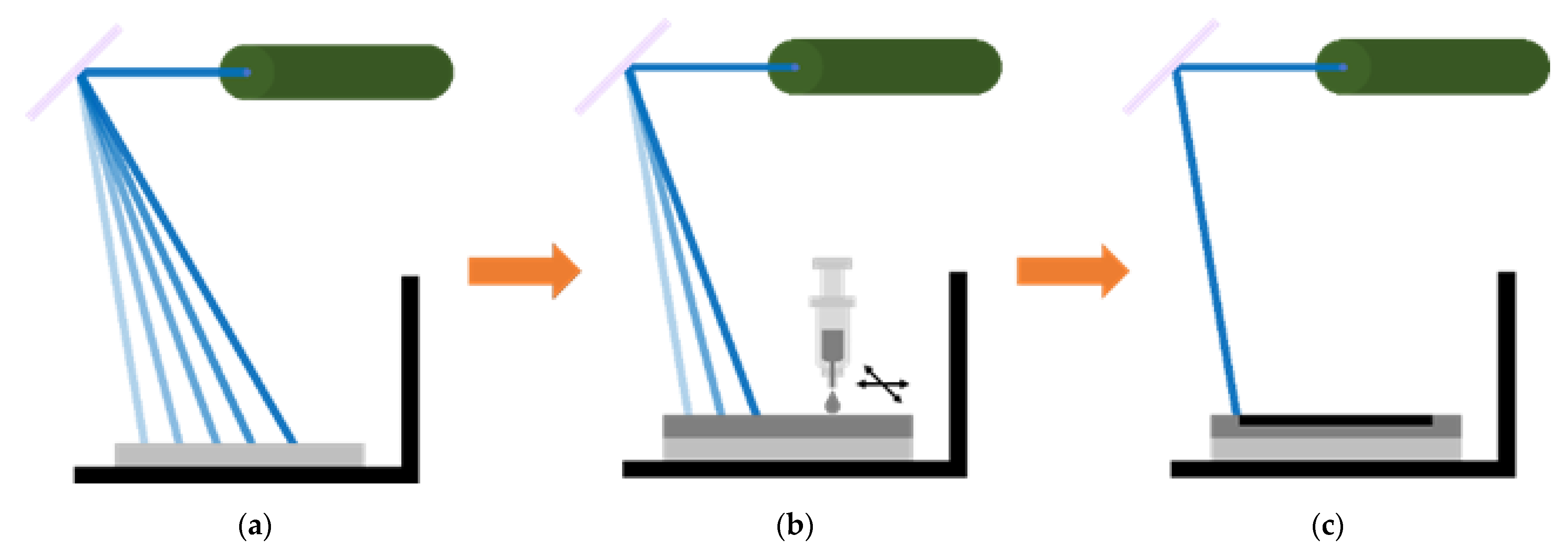
Therefore, in this study, a high-precision shape was made based on PP-type 3D printing and a conductive pattern was selectively formed using a metal composite resin. In particular, as the PP-type 3D printer used UV laser technology, it was possible to directly irradiate a high-power laser without an additional device compared with the other processes. Therefore, if the metal content of the composite resin was maximized and selective local sintering was performed with a high-power laser, it was possible to form a conductive pattern on various shapes with a simple process without an additional wet process such as chemical deposition/cleaning. To this end, in this study, we proceeded with the fabrication of conductive patterns directly on the 3D-printed surface without additional processes through experiments on various variables, ranging from the composition of the metal materials and composite resins suitable for selective local sintering to the process conditions.
3. Results
3.1. Volume Ratio of the Metal Powder
In this study, our goal was to realize a high conductivity by using only 3D-printed metal powder without post-processing such as a deposition process. As it was impossible to add an additional conductive material other than the printed metal, the content of the metal composite resin was very important. In general, the higher the metal content, the more advantageous it was to realize conductivity during the laser sintering; however, the light transmittance and photo-polymerization were difficult, so the strength of the structure was significantly reduced. Therefore, it was necessary to increase the metal content as much as possible at the level where PP 3D printing was still possible. In general, with the powder injection molding (PIM) process, it is known that the powder content can be up to 60 vol%. Accordingly, in this study, as shown in
Figure 2, the rheological properties of the composite resin were visually observed for an aluminum content of 50 to 60 vol%. In the case of 60 vol%, it was difficult to even mix the composite resin due to the high powder content and blading was almost impossible due to the agglomeration of the powders. In the case of 55 vol%, the viscosity was lowered and it was possible to mix the composite resin, but during the actual blading, when pressure was applied, the material was agglomerated by the region and was not evenly spread. On the other hand, in the case of 50 vol%, which is widely used in existing composite resin 3D printing, a smooth flattening process was possible with an appropriate viscosity and flowability and it was confirmed that curing was also possible. Experiments were carried out by fixing the content of the aluminum powder to 50 vol%, which was the maximum content possible for a smooth printing process.
3.2. Laser Scanning Direction
In this study, after printing, a high-energy laser was irradiated on the surface where the polymer and metal coexisted so that the polymer was ablated and the remaining metal was instantaneously locally sintered to obtain the conductivity. In the case of lasers, as a focused-point light source is rapidly moved to irradiate high light energy, the cooling rate varies depending on the scanning direction even at the same energy; thus, the sintering result can vary. This phenomenon is observed more clearly as the irradiation area is widened [
20]. Therefore, in our experiment, as shown in
Figure 3, to form a 20 mm conductive pattern with a line width of 1 mm, the horizontal and vertical scanning directions were irradiated, respectively.
In general laser processing, ablation and rapid cooling by instantaneous high energy rather than melting help to improve the processing precision and minimize the heat-affected layer. However, in the case of sintering, as in this study, sufficient time and temperatures must be secured for an interconnection by heat between the surrounding metal powders when the polymer binder is removed. Otherwise, the metal powder is removed and blown away from the base structure. Therefore, as shown in
Figure 3, when the laser was irradiated in the horizontal scanning direction, irregular over-processing was observed because the polymer binder was ablated, but the remaining aluminum powder was also randomly blown away. On the other hand, in the case of the vertical scanning direction, in which thermal energy was concentrated on a local area, the polymer binder was removed and, at the same time, a proper interconnection occurred by sintering between the surrounding aluminum powders. In the case of the vertical direction, it was confirmed that a sufficient time for interconnection and thermal energy irradiation had been secured.
3.3. Laser Spot Size
The laser used in this experiment could collect energy with a minimum diameter of 20 µm whilst passing through the beam expander and F-theta lens. It was also possible to enlarge the spot size by adjusting the expander ratio and focus position. In general, when a laser is used for ablation, the smaller the spot size, the better the precision. On the other hand, in the case of melting or sintering (such as welding), a spot size that is too small makes it difficult to make an interconnection between materials. In our study, the polymer binder ablation and the metal powder sintering had to be generated at the same time, so it was essential to select an appropriate spot size. Therefore, the results were observed when changing the spot size to 20, 50, and 100 μm whilst the rest of the conditions were fixed.
When the spot size was as small as 20 µm, which was similar to the size of the aluminum powder used, high energy was momentarily concentrated on a narrow area. Therefore, irregular pattern damage, as shown in
Figure 4, was observed due to contractions based on ablation and thermal shock. As a result, the resistance was also measured as an irregular value of over 0.65 Ω∙cm
−1. On the other hand, when the spot size was 50 μm, which was larger than the aluminum powder used, the polymer was removed and the interconnection by sintering between the aluminum powders was properly formed. The resistance also showed a relatively stable value of 0.33 Ω∙cm
−1. However, when the spot size was increased to 100 µm, the energy density was excessively lowered and the polymer binder itself was not sufficiently ablated, so an interconnection between the aluminum powders could not be formed. As a result, a conductive pattern was not formed, making it impossible to measure the resistance value. Based on this, in this study, a 50 µm spot size was selected as an appropriate condition for the binder ablation and metal powder sintering.
3.4. Laser Repetition Rate
If a pulse repetition rate is lowered at the same laser average power, the energy per pulse increases so the ablation tendency is generally strong. On the other hand, if a pulse repetition rate is increased or a CW mode is used, the energy per pulse is reduced, but the heat energy is evenly distributed over the entire area, which is advantageous for welding or sintering. As the equipment used in this experiment did not support the CW mode and only supported a variable pulse mode of 20~90 kHz, the results were observed whilst changing each pulse condition. As a result, when the pulse repetition rate was 40 kHz or less, as shown in
Figure 5, the energy per single pulse was high and machining by laser ablation mainly occurred, making it impossible to form a conductive pattern. When the pulse repetition rate was increased to 60 kHz, the ablation tendency was reduced and an interconnection between the aluminum powders by sintering occurred, but damage to the edge of the line occurred due to the high energy per pulse. However, at a 90 kHz pulse repetition rate, a neat conductive pattern was obtained based on the proper polymer binder ablation and the aluminum powder interconnection by sintering.
3.5. Laser Scan Path Interval
The laser scan path interval is the interval between lines, as shown in
Figure 3, which affects the overlap rate in the pick-feed direction. If the overlap ratio is low, an interconnection between metal powders becomes difficult. Conversely, if the overlap ratio is excessively high, thermal damage to the entire specimen may occur. In this study, because a beam shaper was not separately used, the laser spot followed a Gaussian distribution so the energy distribution of the entire patterning area could only be evenly made when an appropriate overlap ratio was applied. Therefore, we conducted the experiment whilst varying the scan path interval from 1.25 to 50 µm.
When the overlap ratio was low and the scan path interval was 50 μm, only the machined shape was observed, as shown in
Figure 6, because there was almost no sintering effect by heat and only the polymer binder ablation occurred neatly. Even when the path interval was reduced to 25 µm, a sufficient interconnection between the aluminum powders was not formed and irregularly blown-away shapes were observed. When the path interval was reduced to 10 μm or less, the ablation of the polymer binder and sintering between the aluminum powders were simultaneously well-performed, enabling a smooth conductive pattern formation. However, as the path interval decreased, the process time also increased and, as shown in
Figure 6, when excessive light energy was irradiated unnecessarily, we observed that the heat-affected zone at the line edge increased. The IV curves were measured, as shown in
Figure 7, to accurately measure the conductivity change tendency for each condition. When the path interval was greater than 25 µm, as shown in the SEM image, an interconnection between the powders was not formed so the currents were measured as 0, making it impossible to measure the resistance. On the other hand, when the path interval was smaller than 10 μm, the calculated resistance value based on the IV measurement for each process condition was 0.33 to 0.42 Ω∙cm
−1. Although the difference in the resistance value by the process condition was not large, the resistance slightly increased as the path interval decreased. This indicated that the minimum resistance that could be made through the sintering process at a given aluminum powder content was limited to an extent due to the voids between the powders. In addition, it was found that excessive thermal energy caused damage to the surface of the interconnected aluminum powder and adversely affected the resistance reduction. Therefore, in this experiment, the scan path interval for excellent conductivity and low thermal damage was determined to be 10 μm.
3.6. Laser Scanning Speed
If the scan path interval tested previously was used to control the pick-feed interval in the scanning direction, the laser scanning speed was used to change the overlap rate in the feed direction by controlling the moving speed of the spot. Therefore, similar to the scan path interval test results, if the overlap rate was high, excessive thermal effects could be observed and if the overlap rate was low, the interconnection between powders could be insufficient. In this experiment, the results were observed whilst changing the scanning speed from 6.25 to 100 mm/s.
As shown in
Figure 8, when the scanning speed was 100 mm/s, which was a low overlap ratio, an interconnection between the powders was not formed at all and only the ablation phenomenon was observed. On the other hand, when the scanning speed was 50 mm/s or less, it was confirmed that the polymer binder was ablated and an interconnection between the aluminum powders was sufficiently formed to make a conductive pattern. However, as can be seen from the surface and cross-sectional SEM images, thermal damage occurred in the depth direction and the line edge direction due to an excessive thermal energy superposition. Such unnecessary thermal damage causes an increase in resistance, as described above. As shown in
Figure 9, as a result of calculating the resistance using the IV curve, when the scanning speed was slower than 50 mm/s, it could be seen that the resistance was similar or increased due to the unnecessary damage. On the other hand, when the scanning speed was faster than 50 mm/s, the current was measured as 0, so it was impossible to measure the resistance. Therefore, in this study, it was concluded that a scanning speed of 50 mm/s, which formed an excellent conductive pattern whilst minimizing the damage, was the most appropriate.
4. Conclusions
In this study, the possibility of forming a conductive circuit pattern through direct sintering was tested using a composite resin and a laser from PP-type 3D printing. Unlike previous similar studies, the goal was to develop a process that could directly form conductivity from a 3D surface without a separate chemical wet process in a single device.
A composite resin was prepared by variously controlling the type of base resin, the type of metal powder, and the mixing ratio in order to derive the optimal result. Based on this, various laser process conditions were tested so that the polymer binder removal and selective sintering reaction could occur at the same time on the selected 50 vol% aluminum powder composite resin and the results were observed. Each result was evaluated by calculating the resistance value by measuring the IV curve through a potentiostat and analyzing the SEM image. Unlike the laser machining process, in which ablation is the main mechanism, when high-energy density was given by lowering the spot size, repetition rate, path interval, and scanning speed, only damage caused by excessive thermal energy occurred. On the other hand, when the energy density was excessively lowered, an intermetallic interconnection by the appropriate sintering reaction could not be formed, making it impossible to form the conductive pattern. Therefore, in this study, after the 3D printing of the 50 vol% aluminum composite resin, a 0.8 W UV laser was set to a beam spot size of 50 µm and irradiated on the surface. At this time, when the pulse repetition rate, scan path interval, and scanning speed were set to 90 kHz, 10 μm, and 50 mm/s, respectively, an optimal conductive pattern with a resistance of 0.33 Ω∙cm
−1 was obtained. Furthermore, as shown in
Figure 10, the feasibility of the sintered conductive pattern was confirmed by the construction and operation of LEDs using the circuit. The proposed process may contribute to the development of 3D-printed electronics and may enable a simple and inexpensive patterned circuit implementation.


