
Low-Noise Potentiostat Readout Circuit with a Chopper Fully Differential Difference Amplifier for Glucose Monitoring


Abstract
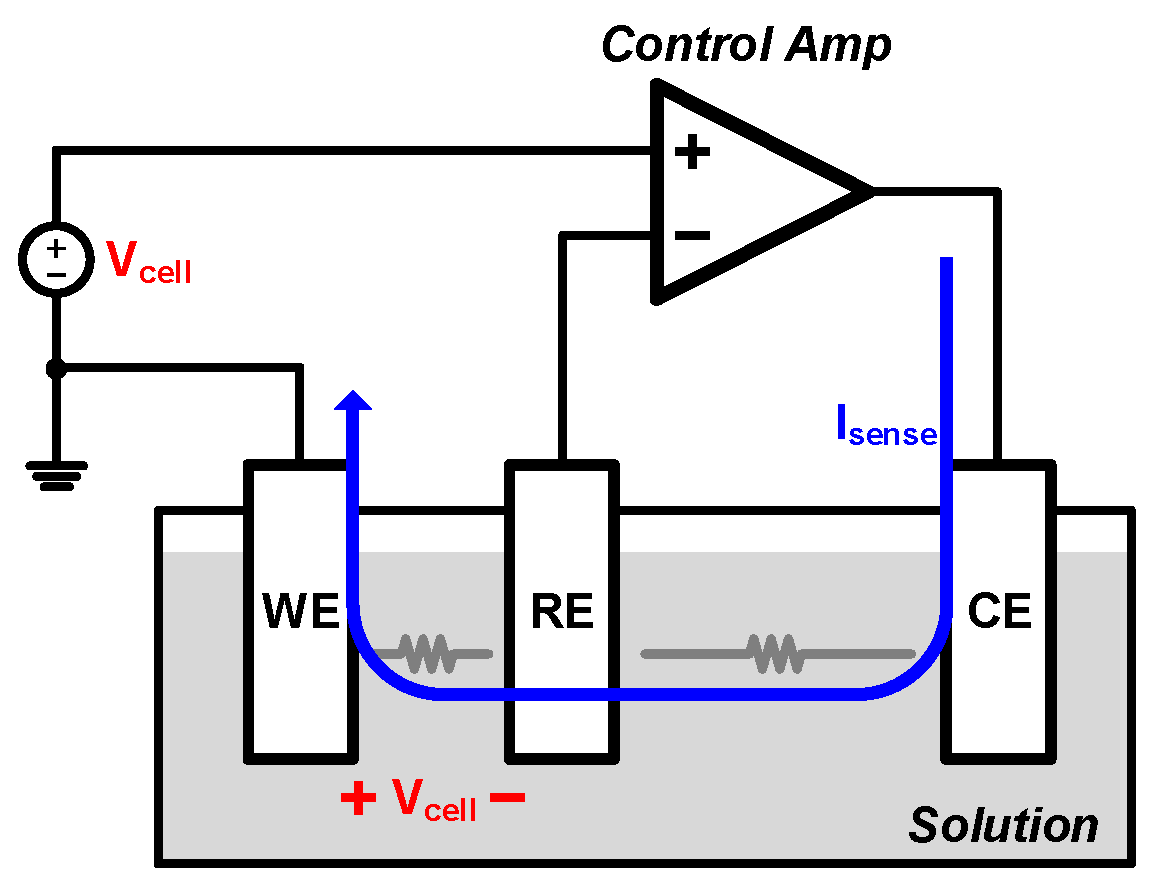
:1. Introduction
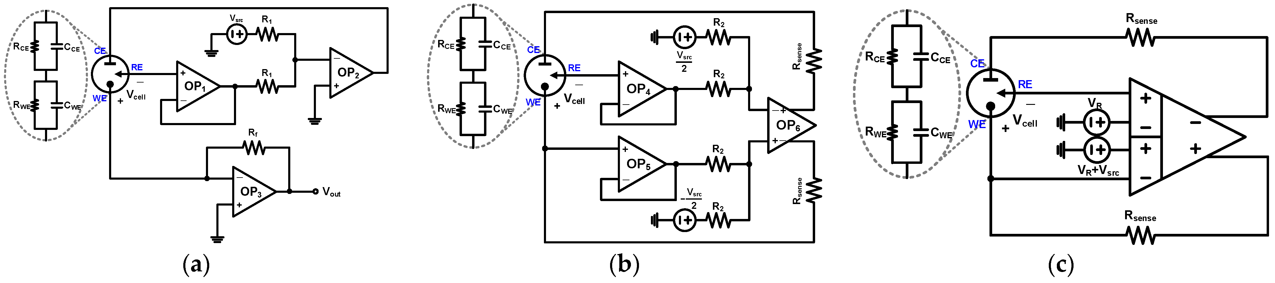
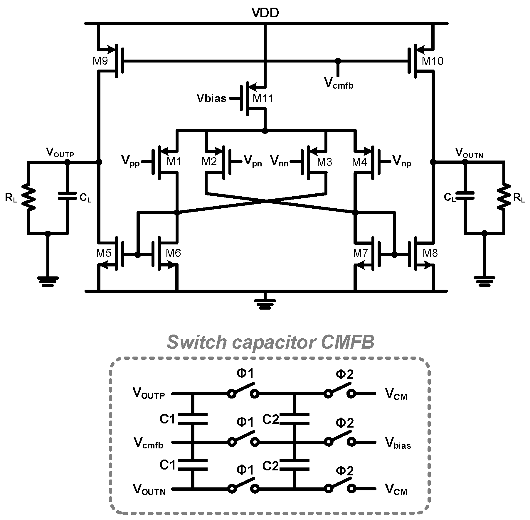
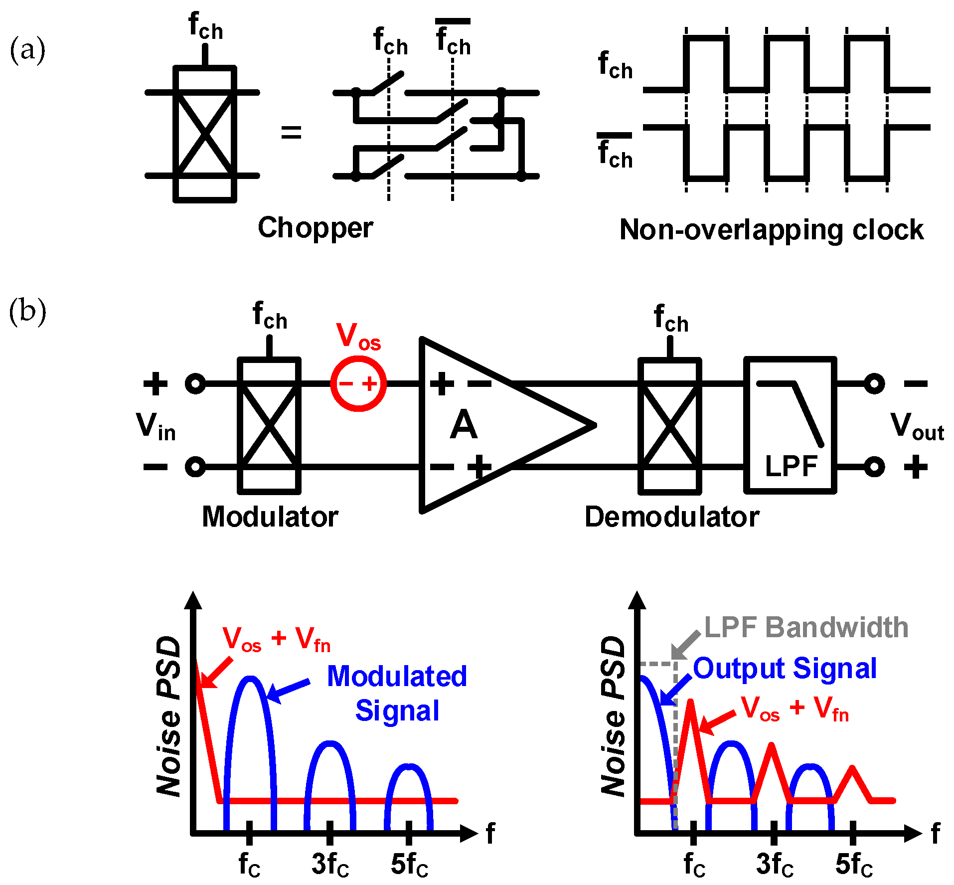
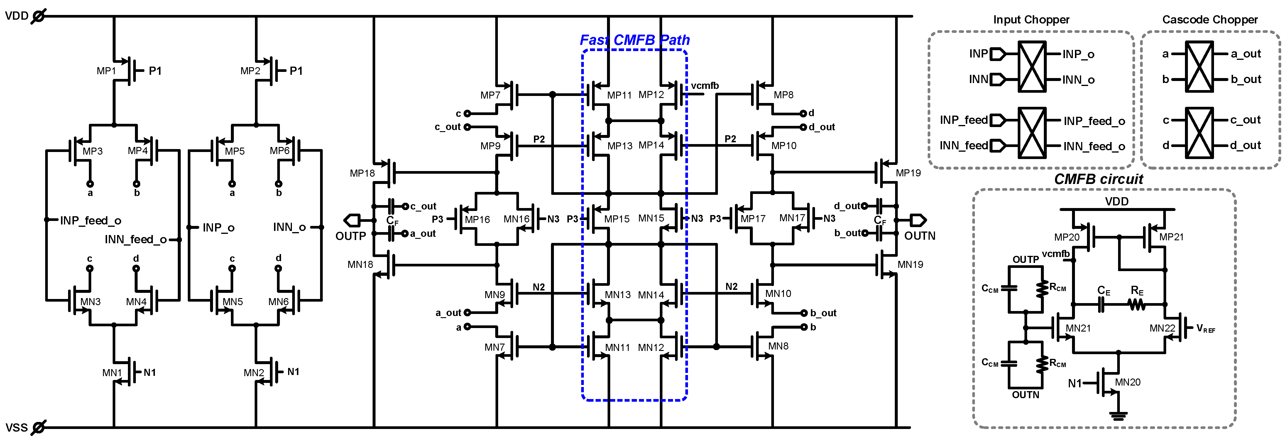
2. Proposed Potentiostat Readout Circuit
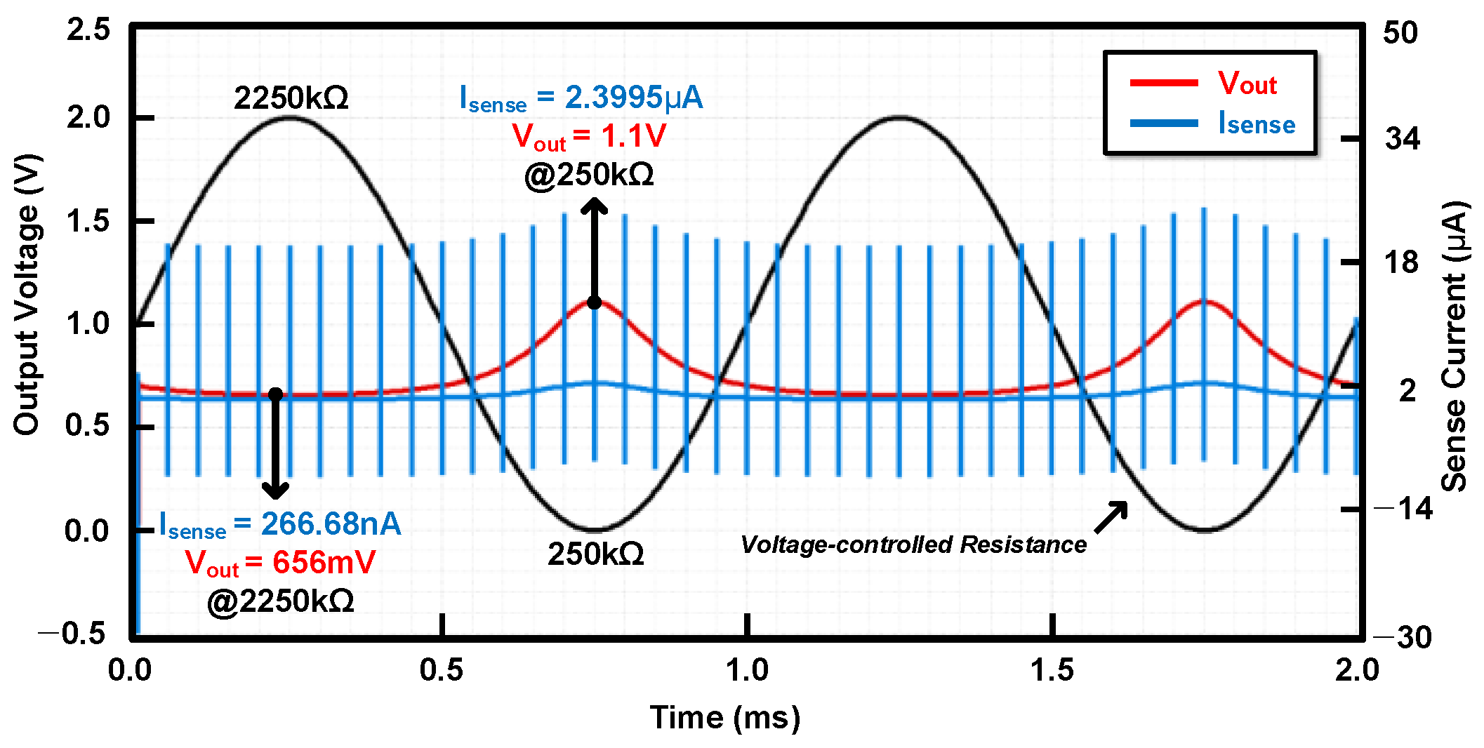
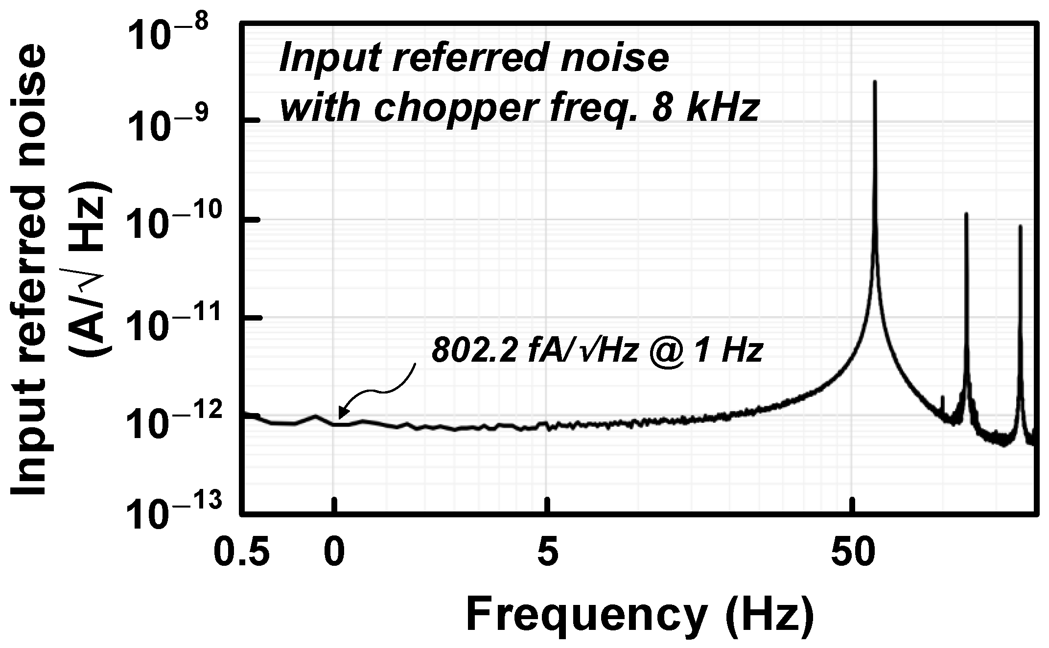
3. Measurement Results
4. Conclusions
Author Contributions
Funding
Institutional Review Board Statement
Informed Consent Statement
Data Availability Statement
Acknowledgments
Conflicts of Interest
References
- Tubiana-Rufi, N.; Riveline, J.-P.; Dardari, D. Real-time continuous glucose monitoring using Guardian®RT: From research to clinical practice. Diabetes Metab. 2007, 33, 415–420. [Google Scholar] [CrossRef] [PubMed]
- Kim, J.; Ko, H. A 1.2 V Low-Power CMOS Chopper-Stabilized Analog Front-End IC for Glucose Monitoring. IEEE Sensors J. 2016, 16, 6517–6518. [Google Scholar] [CrossRef]
- Zuo, L.; Islam, S.K.; Mahbub, I.; Quaiyum, F. A Low-Power 1-V Potentiostat for Glucose Sensors. IEEE Trans. Circuits Syst. II 2015, 62, 204–208. [Google Scholar] [CrossRef]
- Kwon, J.; Lee, Y.; Lee, T.; Ahn, J.-H. Aptamer-Based Field-Effect Transistor for Detection of Avian Influenza Virus in Chicken Serum. Anal. Chem. 2020, 92, 5524–5531. [Google Scholar] [CrossRef] [PubMed]
- Ahmadi, M.M.; Jullien, G.A. Current-Mirror-Based Potentiostats for Three-Electrode Amperometric Electrochemical Sensors. IEEE Trans. Circuits Syst. I Regul. Pap. 2008, 56, 1339–1348. [Google Scholar] [CrossRef]
- De Venuto, D.; Torre, M.D.; Boero, C.; Carrara, S.; De Micheli, G. A Novel Multi-Working Electrode Potentiostat for Electrochemical Detection of Metabolites. In Proceedings of the SENSORS, 2010 IEEE, Waikoloa, HI, USA, 1–4 November 2010; pp. 1572–1577. [Google Scholar]
- De Campos da Costa, J.P.; Bastos, W.B.; da Costa, P.I.; Zaghete, M.A.; Longo, E.; Carmo, J.P. Portable Laboratory Platform with Electrochemical Biosensors for Immunodiagnostic of Hepatitis C Virus. IEEE Sens. J. 2019, 19, 10701–10709. [Google Scholar] [CrossRef]
- Genov, R.; Stanacevic, M.; Naware, M.; Cauwenberghs, G.; Thakor, N. 16-Channel Integrated Potentiostat for Distributed Neurochemical Sensing. IEEE Trans. Circuits Syst. I Regul. Pap. 2006, 53, 2371–2376. [Google Scholar] [CrossRef] [Green Version]
- Schienle, M.; Paulus, C.; Frey, A.; Hofmann, F.; Holzapfl, B.; Schindler-Bauer, P.; Thewes, R. A fully electronic DNA sensor with 128 positions and in-pixel A/D conversion. IEEE J. Solid-State Circuits 2004, 39, 2438–2445. [Google Scholar] [CrossRef]
- Martin, S.M.; Gebara, F.H.; Strong, T.D.; Brown, R.B. A Fully Differential Potentiostat. IEEE Sens. J. 2009, 9, 135–142. [Google Scholar] [CrossRef]
- Wang, W.-S.; Kuo, W.-T.; Huang, H.-Y.; Luo, C.-H. Wide Dynamic Range CMOS Potentiostat for Amperometric Chemical Sensor. Sensors 2010, 10, 1782–1797. [Google Scholar] [CrossRef] [PubMed]
- Ghodsevali, E.; Morneau-Gamache, S.; Mathault, J.; Landari, H.; Boisselier; Boukadoum, M.; Gosselin, B.; Miled, A. Miniaturized FDDA and CMOS Based Potentiostat for Bio-Applications. Sensors 2017, 17, 810. [Google Scholar] [CrossRef] [PubMed] [Green Version]
- Menolfi, C.; Huang, Q. A Fully Integrated, Untrimmed CMOS Instrumentation Amplifier with Submicrovolt Offset. IEEE J. Solid-State Circuits 1999, 34, 415–420. [Google Scholar] [CrossRef]
- Monticelli, D.M. A quad CMOS single-supply op amp with rail-to-rail output swing. IEEE J. Solid-State Circuits 1986, 21, 1026–1034. [Google Scholar] [CrossRef] [Green Version]
- Jun, J.; Park, S.; Kang, J.; Kim, S. A 22-bit Read-Out IC with 7-ppm INL and Sub-100 μHz 1/f Corner for DC Measurement Systems. IEEE J. Solid-State Circuits 2019, 54, 3086–3096. [Google Scholar] [CrossRef]
- Anoop, A.E.; Mohan, N.M.; Guruvayurappan, K. Simulation of a multi-strip blood glucometer. In Proceedings of the TENCON 2014–2014 IEEE Region 10 Conference, Bangkok, Thailand, 22–25 December 2014; pp. 1–4. [Google Scholar] [CrossRef]
- Aymerich, J.; Marquez, A.; Munoz-Berbel, X.; Del Campo, F.J.; Guirado, G.; Teres, L.; Serra-Graells, F.; Dei, M. A 15-μW 105-dB 1.8-Vpp Potentiostatic Delta-Sigma Modulator for Wearable Electrochemical Transducers in 65-nm CMOS Technology. IEEE Access 2020, 8, 62127–62136. [Google Scholar] [CrossRef]
- Al Mamun, K.A.; McFarlane, N. A CMOS potentiostatic glucose monitoring system for VACNF amperometric biosensors. In Proceedings of the 2015 IEEE International Symposium on Circuits and Systems (ISCAS), Lisbon, Portugal, 24–27 May 2015; pp. 477–480. [Google Scholar] [CrossRef]
- Toprak, S.; Vural, R.A.; Batur, O.Z. Low Noise High Linearity Current Readout Topologies for Potentiostat Circuitry. In Proceedings of the 2021 IEEE 32nd International Conference on Microelectronics (MIEL), Niš, Serbia, 12–14 September 2021; pp. 219–222. [Google Scholar]
- Ahmad, R.; Joshi, A.M.; Boolchandani, D.; Varma, T. Design of Potentiostat and Current Mode Read-out Amplifier for Glucose Sensing. In Proceedings of the 2021 IEEE International Symposium on Smart Electronic Systems (iSES), Jaipur, India, 20–22 December 2021; pp. 64–69. [Google Scholar]


| Transistor | Size (W/L) (μm) | Transistor | Size (W/L) (μm) |
|---|---|---|---|
| MP1, MP2 | 60/2.5 | MN1, MN2 | 16/4 |
| MP3–MP6 | 40/0.5 | MN3–MN6 | 40/0.5 |
| MP7, MP8 | 20/2 | MN7, MN8 | 16/4 |
| MP9, MP10 | 160/0.5 | NM9, MN10 | 80/0.5 |
| MP11 | 5/2 | MN11, MN12 | 4/4 |
| MP12 | 50/2 | MN13, MN14 | 20/0.5 |
| MP13, MP14 | 40/0.5 | MN15 | 5/4 |
| MP15 | 200/2 | MN16, MN17 | 5/4 |
| MP16, MP17 | 80/2 | MP18, MP19 | 5/0.5 |
| MP18, MP19 | 10/0.5 | MN20 | 4/2 |
| MP20, MP21 | 12/5 | MN21, MN22 | 40/0.5 |
| Component | Value |
|---|---|
| CF | 4.8 pF |
| CCM | 412 fF |
| RCM | 562.615 kΩ |
| CE | 3.2 pF |
| RE | 1 MΩ |
| Test Strip Name | Glucose Conc. Range (mg/dL) | Resistance (kΩ) | |
|---|---|---|---|
| Minimum | Maximum | ||
| Optimum®, Abbott | 46–393 | 4.58 | 5.64 |
| Contour®, Bayer | 34–522 | 35.71 | 500 |
| OneTouch Ultra®, Johnson & Johnson | 36–450 | 250 | 2000 |
| This Work | IEEE MIEL 2021 [19] | IEEE iSES 2021 [20] | IEEE Access 2020 [17] | Sensors 2017 [13] | ISCAS 2015 [18] | |
|---|---|---|---|---|---|---|
| Process (μm) | 0.18 | 0.18 | 0.18 | 0.065 | 0.18 | 0.18 |
| Architecture | FDDA | Current conveyer | Current conveyer | 1st-order delta-sigma converter | FDDA | DDA |
| Chopper | Y (8 kHz) | N | N | N | N | N |
| Output format | Voltage | Current | Voltage | Digital codes | Voltage | Voltage |
| Supply voltage (V) | 1.8 | 1.8 | 1.5 | 1.2 | 1.8 | 1.8 |
| Power consumption (μW) | 86.4 | 2300 | 124 | 15–25 (0.1–1.5 μA) | 53 | 72.36 |
| Input-referred noise (pARMS) | 11.2 (50 Hz BW) (measured) | 153 (0.01~1 kHz) | N/A | 168.3 1 (1 Hz BW) (measured) | N/A | N/A |
Publisher’s Note: MDPI stays neutral with regard to jurisdictional claims in published maps and institutional affiliations. |
© 2022 by the authors. Licensee MDPI, Basel, Switzerland. This article is an open access article distributed under the terms and conditions of the Creative Commons Attribution (CC BY) license (https://creativecommons.org/licenses/by/4.0/).
Share and Cite
Choi, G.; Nam, K.; Yoo, M.; Kang, S.; Jin, B.; Kim, K.; Son, H.; Ko, H. Low-Noise Potentiostat Readout Circuit with a Chopper Fully Differential Difference Amplifier for Glucose Monitoring. Appl. Sci. 2022, 12, 11334. https://doi.org/10.3390/app122211334
Choi G, Nam K, Yoo M, Kang S, Jin B, Kim K, Son H, Ko H. Low-Noise Potentiostat Readout Circuit with a Chopper Fully Differential Difference Amplifier for Glucose Monitoring. Applied Sciences. 2022; 12(22):11334. https://doi.org/10.3390/app122211334
Chicago/Turabian StyleChoi, Gyuri, Kyeongsik Nam, Mookyoung Yoo, Sanggyun Kang, Byeongkwan Jin, Kyounghwan Kim, Hyeoktae Son, and Hyoungho Ko. 2022. "Low-Noise Potentiostat Readout Circuit with a Chopper Fully Differential Difference Amplifier for Glucose Monitoring" Applied Sciences 12, no. 22: 11334. https://doi.org/10.3390/app122211334