Abstract
Recently, great advances had been made by using scanning probe microscopy (SPM) to quantify the relative permittivity of thin film materials on a nanometer scale. The imaging techniques of permittivity for thin film materials with SPM, especially for photoelectric materials, have not been fully researched until now. Here, we presented a method to image permittivity of thin film materials by using a scanning capacitance microscope (SCM). This method combined the quantitative measurement by using SCM with the capacitance gradient–distance fitting curve to obtain the two-dimensional (2D) permittivity image at room temperature under atmospheric conditions. For the demonstration, a 2D permittivity image of film of molybdenum oxide (MoO3), a kind of photoelectric material, was acquired. From the image, it could be found that the average values of permittivity of MoO3 film and of MoO3 film-doped NaCl were about 8.0 and 9.5, respectively. The experimental results were quantitatively consistent with other experimental results of the same material. The reported technique here could provide a novel method for imaging the relative permittivity with nanometer resolution and be helpful for the study of photoelectric materials.
1. Introduction
Since the invention of the scanning tunneling microscope (STM) by G. Binnig et al. in August 1981, [1] it has been widely used in the research of physics, chemistry, biology, material science and other fields. Additionally, a large family, called scanning probe microscopy (SPM), has been derived. Atomic Force Microscope (AFM) was a kind of SPM. AFM could be used to explore the nanomechanical properties of soot particle layers [2]. A developed ultrasonic AFM was used to measure the sub-surface microstructures [3].
Scanning capacitance microscope (SCM) was an important member of the SPM family [4]. In September 1981, J. R. Matey filed a patent application related to SCM [5]. In 1998, J. Kopanski et al. used tapping AFM to realize intermittent contact mode SCM. It could image the metal lines buried under a 1-μm thick dielectric film [6].
Great advances have been made by using SPM to quantify the relative permittivity εr of thin film materials on the nanometer scale [7]. In 2015, E. Bussmann et al. used SCM to determine the subsurface of electronic devices in silicon layer. The electronic device was covered with 10–100-nm thick silicon [8]. In 2019, J. Xu et al. measured the capacitance gradient between the tip and the sample through electrostatic force [9]. It was an instrument that could not only image the surface, but also image the internal inhomogeneity of semiconductors or dielectric materials. It was considered to be a promising tool for high-resolution and high-precision analysis of doping concentration and dielectric properties in semiconductor material. In recent ten years, people had made great efforts to achieve this goal. Then, by using image method, they established the theoretical mode, and deduced the permittivity of the sample [10].
There were previous applications of measuring the dielectric properties of films by means of SCM or electrostatic force combined with a theoretical model. However, there was no direct method to measure the relative permittivity εr of dielectric films by SCM. Furthermore, a variety of studies have been conducted, but the imaging techniques of εr for thin film materials with SPM, especially for photoelectric materials, had not been fully researched until now. In this paper, the experiment and numerical fittings were used to directly measure the εr distribution of the film by using SCM at room temperature under an atmospheric condition.
This method combined the quantitative measurement by using SCM with the capacitance gradient–distance fitting curve to obtain the two-dimensional (2D) image of εr. There were four steps in the method as following:
Step 1. A capacitance gradient ~distance z curve was acquired on a metal ground. The capacitance gradient was the gradient of the capacitance between the tip and the metal ground. The distance was the tip-metal ground distance. Then, the effective tip parameters (such as tip radius R = R0, cone half angle θ = θ0, and stray capacitance constant ) could be determined by means of fitting [11,12].
Step 2. A capacitance gradient ~distance z curve was acquired on a monocrystalline silicon (Si) substrate ground. The capacitance gradient was the gradient of the capacitance between the tip and the Si substrate ground. The distance was the tip-Si substrate ground distance. The curve was fitted with R = R0 and θ = θ0, the stray capacitance constant could be determined. Usually, there were ≠ , and ≈ , where was the stray capacitance constant when an insulating film was coated on the Si substrate ground.
Step 3. When an insulating film with thickness h and relative permittivity εr was coated on the Si substrate ground, each line was scanned two times. The topography image and SCM image (with the tip lifted to a proper height z’) were acquired almost at the same time.
Step 4. From the SCM image, every signal of SCM could be changed to the value of at the corresponding point. By using R0, θ0, z’, and et al. for data reconstruction, every value of could be changed to the value of h/εr at the corresponding point. The topography image was used to determine the thickness of the film at every point. Then, at every point was synthesized and the 2D distribution of on the nanometer scale could be obtained.
This method of measuring permittivity of thin films can be applied to semiconductor materials and photoelectric materials, obtaining the two-dimensional doping type and doping level distribution, and providing an effective tool for manufacturing process testing such as semiconductor devices and optical appliances. In addition, this method plays an important role in photonics in different applications [13].
2. Materials and Methods
2.1. Principles
By considering the tip as a point-mass spring, the equation of motion for the tip could be represented as [14]:
where m denoted the effective mass, K the spring constant, the displacement of the tip from the equilibrium position, Q the quality factor, the free resonance angular frequency, Fts the tip-surface interaction, F0 and ωd the amplitude and angular frequency of the driving force, respectively.
The tip-surface interaction may consist of various contributions, such as short range repulsive and chemical binding forces, van der Waals force FvdW, and long-range electrostatic and magnetic forces, Fel and Fmag, respectively. When the tip was lifted to a proper height z, the influence of van der Waals force on the tip could be negligible, [15] and the tip vibrated completely under the long-range electrostatic and magnetic forces, Fel and Fmag.
When both the tip and the sample were conductive materials, the tip and the sample formed a capacitance C. If a DC voltage and an AC voltage were applied between the tip and the sample, the voltage between the tip and the sample was
where was the surface potential of the sample.
The energy stored in this capacitor was
The force on the tip was
Then the force between the tip and the sample was [15]
where the spectral components were:
When the tip was lifted to a proper height , the tip vibrated completely under the electric field force. If the frequency of the AC voltage applied to the tip was half of the resonance frequency of the cantilever, the tip was under the drive of . The vibration equation was
When the amplitude of the tip was very small, the influence of vibration on ∂C/∂z could be ignored, where C was the capacitance between the tip and the sample. The solution of Equation (9) was
It could be seen from Equation (10) that the amplitude of the cantilever was proportional to the capacitance gradient ∂C/∂z when the amplitude was very small.
The measured capacitance variation with respect to reference distance was [7]
and
where was the apex capacitance contribution including both the dielectrics and the tip shape effect, and was the stray capacitance between the cantilever and the ground.
The stray contribution could be precisely quantified as [16,17]
by linearly fitting the region where the effect of the apex capacitance was negligible. In Equation (13), stray capacitance constant kstray was determined by the structure between the cantilever and the ground.
From Equation (10), the capacitance gradient ∂C/∂z was represented with the vibration amplitude. In the region where the effect of the apex capacitance was negligible, the measured capacitance gradient should be
With tip radius R and cone half angle θ, S. Hudlet et al. studied the capacitance between the tip and a metallic surface. The apex capacitance was given by [18]
Its capacitance gradient was
Then, the should be fitted in the apex capacitance region by
Detecting the capacitance gradient vs. setting height z between the tip and a metal ground, the tip radius R = R0, cone half angle θ = θ0, and stray capacitance constant could be obtained by fitting ~z curve with Equation (17).
When an insulating film with thickness h and relative permittivity εr was coated on the metal ground, L. Fumagalli et al. proposed to use equivalent instead of z in Equation (15) to calculate the capacitance. The apex capacitance was proposed to be [7]
Its apex capacitance gradient was
Then, the could be fitted in the apex capacitance region by
When an insulating film was coated on the metal (or monocrystalline silicon substrate) ground, the value of for ground (marked with ) could be obtained by fitting ~z curve with tip radius R0, cone half angle θ0, and Equation (17) above. The value of could be approximately replaced by that of . The value of was usually different from that of .
Double scanning technology was used to acquire the topography image and SCM image (with the tip lifted to a proper height z’). A procedure of 1 Order (line-by-line subtraction of the first order approximating curve) was selected, the detection signal was corrected for the tilt contribution. The value of of every point could be obtained from the SCM image by using R0, θ0, , and Equation (20) above for data reconstruction. The value of h of the insulating film at every point could be obtained from the topography image. Then, the value of relative permittivity εr of every point could be calculated, and the 2D distribution of on the nanometer scale could be acquired.
2.2. Methods
In the present paper, an SPM instrument of a Russian NT-MDT company was used in the experiment. The SCM mode of SPM was used to quantitatively measure the molybdenum trioxide (MoO3) film at room temperature under atmospheric condition. The MoO3 film was partially doped with sodium chloride (NaCl) and based on monocrystalline silicon (Si).
The SCM mode could measure the capacitance gradient vs. setting height z curve with high resolution for metal ground and for Si substrate ground. Using the above tip sample capacitance gradient model, the tip radius R0, cone half angle θ0, and could be obtained from the ~z curve. With R0 and θ0, could be obtained from ~z curve. There was ≈ , where was the stray capacitance constant when an insulating film was coated on the Si substrate ground.
Then, double scanning technology was used on the sample to image. The double scanning technology scanned each line two times in the scanning process. The first scanning was to scan the topography of the sample, and its scanning parameters were exactly the same as those of ordinary semi contact scanning. A procedure of 1 Order (line-by-line subtraction of the first order approximating curve) was selected, and the detection signal was corrected for the tilt contribution. In the second scanning, the tip was lifted to a proper height z’. The influence of van der Waals force on the tip could be negligible, and the tip vibrated completely under the electric field force. The second scanning was SCM scanning. It was performed on the same line just after the first scanning. In the second scanning, a 1 V AC sinusoidal signal with frequency , was loaded between the tip and the monocrystalline silicon substrate. The feedback loop of the system was closed. The amplitude of the tip was detected, and the capacitance gradient could be obtained. The topography scanning and the SCM scanning were finished almost at the same time.
3. Results
This section may be divided by subheadings. It should provide a concise and precise description of the experimental results, their interpretation, as well as the experimental conclusions that can be drawn.
First, in order to determine the parameters (the tip radius R and the cone half angle θ) of the tip, the capacitance gradient vs. setting height z curve for metal ground was measured. The tip was set to touch the metal ground and then was lifted to a proper height z automatically. The measured capacitance gradient vs. setting height z between the tip and the metal ground was shown in Figure 1. Fitted with Equation (17) by using Origin 2021, the tip radius R = R0 = 16.6 nm, cone half angle θ = θ0 = 20°, and the constant = 0.039 aF/nm could be obtained. Packaging specification of the probe was tip radius R ≤ 10 nm and cone half angle θ ≤ 22°. Since the probe was used for some time and may be blunt, the tip radius R0 = 16.6 nm, and cone half angle θ0 = 20° were reasonable.
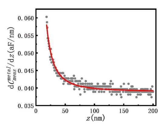
Figure 1.
The measured capacitance gradient vs. setting height z and its fitted curve.
The monocrystalline silicon substrate partly coated with MoO3 film was grounded. A point of Si substrate area was chosen, and its measured capacitance gradient vs. setting height z between tip and Si ground was shown in Figure 2. Fitted with R0 = 16.6 nm, θ0 = 20° and Equation (18), the constant = 0.043 aF/nm could be obtained. The value of approximately was 0.043 aF/nm, and it was larger than that of .
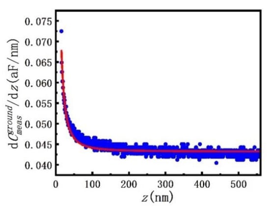
Figure 2.
The measured capacitance gradient vs. setting height z and its fitted curve.
Double scanning technology was performed on the sample. A procedure of 1 Order (line-by-line subtraction of the first order approximating curve) was selected, the detection signal was corrected for the tilt contribution. In the second scanning, the tip is lifted to a height z’ = 10 nm. The topography image and SCM image of the sample was shown in Figure 3a,b, respectively. The different area was marked in Figure 3a.
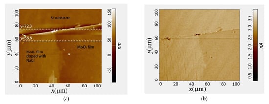
Figure 3.
(a) the topography image of the sample and (b) the SCM image with z’ = 10 nm.
From Figure 3a, the profiles for y = 56.6 μm and y = 72.3 μm (mark in Figure 3a) were exported as shown in Figure 4a,b, respectively.
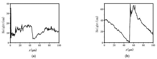
Figure 4.
The height profiles for (a) y = 56.6 μm and (b) y = 72.3 μm of the topography image.
Compared with Figure 3, it could be seen from Figure 4a that the fall from 17 nm to 4 nm at x ≈ 45 μm corresponded to the change from MoO3 film-doped NaCl to MoO3 film. It meant that the film of MoO3-doped NaCl was 13 nm thicker than that of MoO3.
Compared with Figure 3, it could be seen from Figure 4b that the rise of 70 nm at x ≈ 52 μm corresponded to the change from monocrystalline Si substrate to MoO3 film. Then, the average thickness of the film could be set as 70 nm. From the topography image of the film, the rise and fall of every point could be regarded as the thickness change . The thickness of the film at every point could be set as . The thickness profile for y = 56.6 μm was shown in Figure 5a. Additionally, the SCM profile for y = 56.6 μm from Figure 5 was shown in Figure 5b.
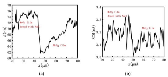
Figure 5.
(a) The thickness and (b) the SCM profiles for y = 56.6 μm.
It could be seen from Figure 5a that there was a fall from 75 nm to 62 nm at x ≈ 45 μm. The drop corresponded to the change from MoO3 film-doped NaCl to MoO3 film. From Figure 6b, it could be seen that the signal of SCM of MoO3 film was slightly weaker than that of MoO3 film-doped NaCl. The doped NaCl changed the thickness and capacitance of the film.
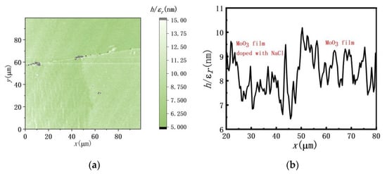
Figure 6.
(a) The 2D image of h/εr and (b) its profile for y = 56.6 μm.
If the value of h/εr of the film at every point could be obtained from the SCM image, the value of εr of the film at every point could be calculated with . The 2D image of the relative permittivity εr could be obtained.
From Figure 3b, every signal of SCM could be changed to the value of at the corresponding point. By using R0 = 16.6 nm, θ0 = 20°, z’ = 10 nm, = 0.043 aF/nm, and Equation (20) above for data reconstruction., every value of could be changed to the value of h/εr at the corresponding point. Then, the SCM image (shown in Figure 4) was reconstructed to the 2D image of h/εr (shown in Figure 6a). Figure 6b shows its profile for y = 56.6 μm.
It could be seen from Figure 6a,b that the value of h/εr of MoO3 film was slightly larger than that of MoO3 film-doped NaCl.
From Figure 6a, every value of h/εr could be changed to the value of εr with above at the corresponding point of Figure 3. Then, the 2D image of εr could be obtained (shown in Figure 7a). Figure 7b was its profile for y = 56.6 μm
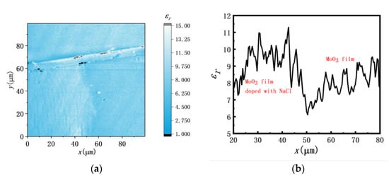
Figure 7.
(a) The 2D image of εr and (b) its profile for y = 56.6 μm.
4. Discussion
- (1)
- With relative density (ρ) ~76.8% of MoO3 dielectric ceramics, the relative permittivity (εr) was ~8.31 [19]. The relative permittivity (εr) of 4.50 M NaCl solution was 32.2 [20]. In the present paper, MoO3 film-doped NaCl was treated with NaCl solution. The average value of εr of MoO3 film was about 8.0, and that of MoO3 film-doped NaCl was about 9.5. The experimental result of MoO3 were quantitatively consistent with other experimental results of the same material, the permittivity (εr) of MoO3-doped NaCl is significantly different from that of the undoped MoO3.
- (2)
- The packaging specification of the probe is tip radius R ≤ 10 nm and cone half angle θ ≤ 22°. The capacitance gradient vs. setting height z between the tip and the metal ground was measured. Fitted with Equation (17), the tip radius R = 16.6 nm and cone half angle θ = 20° were obtained. Since the probe was used for some time and may be blunt, the tip radius R =16.6 nm, and cone half angle θ = 20° were reasonable.
- (3)
- Similar to the chemical intercalation method [21], partial MoO3 film was treated with NaCl solution. There may be Na intercalation in MoO3-film doped NaCl. That was why the thickness and signal of SCM of MoO3 film was slightly weaker than that of MoO3 film-doped NaCl.
- (4)
- From the topography image of the film, the rise and fall of every point was regarded as the thickness change . The thickness of the film at every point was set as . The value of was obtained from the rise of 70 nm, which corresponded to the change from monocrystalline Si substrate to MoO3 film. In the topography image of the film, the rise and fall of every point was relative to the previous point, not relative to 70nm. The value of thickness was an approximate one.
- (5)
- The monocrystalline silicon substrate was partly coated with MoO3 film. A point of Si substrate area was chosen. Its measured capacitance gradient vs. setting height z between the tip, and the Si ground was just used to determine the constant , since Equation (17) was for metal ground.
- (6)
- There was no film on the area of Si substrate in Figure 3a. The results of h and εr of Si substrate area should be ignored.
5. Conclusions
By using the double scanning technology, the topography and SCM images of the sample could be obtained almost at the same time. From the topography image of the film, the rise and fall of every point corresponded to the thickness change . The thickness of the film at every point could be set as . Every signal of SCM could be changed to the value of at the corresponding point. With the tip radius R, and cone half angle θ, etc., the SCM image could be reconstructed to the 2D h/εr image. Then, the two-dimensional (2D) image of the relative permittivity could be acquired. The average value of εr of MoO3 film was about 8.0, and that of MoO3 film-doped NaCl was about 9.5. The experimental results were quantitatively consistent with other experimental results of the same material. The technique could provide a novel method for imaging the relative permittivity with nanometer resolution and be helpful for the study of photoelectric materials.
Author Contributions
Conceptualization, X.D. and G.L.; data curation, Y.L. and T.C.; formal analysis, Y.L.; funding acquisition, X.D.; investigation, Y.L.; methodology, X.D.; writing—original draft, G.L. and Y.L.; writing—review and editing, T.S. and D.C. All authors have read and agreed to the published version of the manuscript.
Funding
This work was supported by the National Natural Science Foundation of China (Grant No. 61871410).
Institutional Review Board Statement
Not applicable.
Informed Consent Statement
Not applicable.
Data Availability Statement
The data presented in this study are available on request from the corresponding author.
Acknowledgments
The authors acknowledge Haojie LAI for preparing the sample, and Weiguang Xie for helpful discussion about the experiment.
Conflicts of Interest
The authors declare no conflict of interest.
References
- Binnig, G.; Rohrer, H.; Gerber, C.; Weibel, E. Tunneling through a Controllable Vacuum Gap. Appl. Phys. Lett. 1982, 40, 178–180. [Google Scholar] [CrossRef]
- Falco, G.D.; Carbone, F.; Commodo, M.; Minutolo, P.; D’Anna, A. Exploring Nanomechanical Properties of Soot Particle Layers by Atomic Force Microscopy Nanoindentation. Appl. Sci. 2021, 11, 8448. [Google Scholar] [CrossRef]
- Wang, Y.Y.; Wu, C.J.; Tang, J.Y.; Duan, M.Y.; Chen, J.; Ju, B.-F.; Chen, Y.-L. Measurement of Sub-Surface Microstructures Based on a Developed Ultrasonic Atomic Force Microscopy. Appl. Sci. 2022, 12, 5460. [Google Scholar] [CrossRef]
- Matey, J.R.; Blance, J. Scanning capacitance microscopy. J. Appl. Phys. 1985, 57, 1437–1444. [Google Scholar] [CrossRef]
- Matey, J.R. Scanning Capacitance Microscope. U.S. Patent 4,481,616, 6 November 1984. [Google Scholar]
- Kopanski, J.J.; Mayo, S. Intermittent-contact scanning capacitance microscope for lithographic overlay measurement. Appl. Phys. Lett. 1998, 72, 2469–2471. [Google Scholar] [CrossRef]
- Fumagalli, L.; Ferrari, G.; Sampietro, M.; Gomila, G. Dielectric-constant measurement of thin insulating films at low frequency by nanoscale capacitance microscopy. Appl. Phys. Lett. 2007, 91, 243110. [Google Scholar] [CrossRef]
- Bussmann, E.; Rudolph, M.; Subramania, G.S.; Misra, S.; Carr, S.M.; Langlois, E.; Dominguez, J.; Pluym, T.; Lilly, M.P.; Carroll, M.S. Scanning capacitance microscopy registration of buried atomic-precision donor devices. Nanotechnology 2015, 26, 085701. [Google Scholar] [CrossRef]
- Xu, J.; Li, J.Z.; Li, W. Calculating electrostatic interactions in atomic force microscopy with semiconductor samples. AIP Adv. 2019, 9, 105308. [Google Scholar] [CrossRef]
- Gramse, G.; Gomila, G.; Fumagalli, L. Quantifying the dielectric constant of thick insulators by electrostatic force microscopy: Effects of the microscopic parts of the probe. Nanotechnology 2012, 23, 205703. [Google Scholar] [CrossRef]
- Gomila, G.; Toset, J.; Fumagalli, L. Nanoscale capacitance microscopy of thin dielectric films. J. Appl. Phys. 2008, 104, 024315. [Google Scholar] [CrossRef]
- Fumagalli, L.; Gramse, G.; Esteban-Ferrer, D.; Edwards, M.A.; Gomila, G. Quantifying the dielectric constant of thick insulators using electrostatic force microscopy. Appl. Phys. Lett. 2010, 96, 183107. [Google Scholar] [CrossRef]
- Mahariq, I.; Kurt, H. On- and off-optical-resonance dynamics of dielectric microcylinders under plane wave illumination. J. Opt. Soc. Am. B 2015, 32, 1022–1030. [Google Scholar] [CrossRef]
- García, R.; Pérez, R. Dynamic atomic force microscopy methods. Surf. Sci. Rep. 2002, 47, 197–301. [Google Scholar] [CrossRef]
- Sadewasser, S.; Glatzel, T. Kelvin Probe Force Microscopy-From Single Charge Detection to Device Characterization. In Springer Series in Surface Sciences; Springer: Berlin/Heidelberg, Germany, 2018; Volume 65. [Google Scholar]
- Lee, D.T.; Pelz, J.P.; Bhushan, B. Instrumentation for direct, low frequency scanning capacitance microscopy, and analysis of position dependent stray capacitance. Rev. Sci. Instrum. 2002, 73, 3525–3533. [Google Scholar] [CrossRef]
- Fumagalli, L.; Ferrari, G.; Sampietro, M.; Casuso, I.; Martinez, E.; Samitier, J.; Gomila, G. Nanoscale capacitance imaging with attofarad resolution using ac current sensing atomic force microscopy. Nanotechnology 2006, 17, 4581–4587. [Google Scholar] [CrossRef] [PubMed]
- Hudlet, S.; Saint Jean, M.; Guthmann, C.; Berger, J. Evaluation of the capacitive force between an atomic force microscopy tip and a metallic surface. Eur. Phys. J. B 1998, 2, 5–10. [Google Scholar] [CrossRef]
- Zhou, D.; Pang, L.-X.; Wang, D.-W.; Reaney, I.M. Novel water-assisting low firing MoO3 microwave dielectric ceramics. J. Eur. Ceram. Soc. 2019, 39, 2374–2378. [Google Scholar] [CrossRef]
- Chandra, A. Static dielectric constant of aqueous electrolyte solutions: Is there any dynamic contribution? J. Chem. Phys. 2000, 113, 903–905. [Google Scholar] [CrossRef]
- Voiry, D.; Yamaguchi, H.; Li, J.; Silva, R.; Alves, D.C.; Fujita, T.; Chen, M.; Asefa, T.; Shenoy, V.B.; Eda, G.; et al. Enhanced catalytic activity in strained chemically exfoliated WS2 nanosheets for hydrogen evolution. Nat. Mater. 2013, 12, 850–855. [Google Scholar] [CrossRef]


Publisher’s Note: MDPI stays neutral with regard to jurisdictional claims in published maps and institutional affiliations. |
© 2022 by the authors. Licensee MDPI, Basel, Switzerland. This article is an open access article distributed under the terms and conditions of the Creative Commons Attribution (CC BY) license (https://creativecommons.org/licenses/by/4.0/).