
Seventy-Five Years since the Point-Contact Transistor: Germanium Revisited


 ,
, 
Abstract
:1. Introduction
2. Transistors and Artificial Intelligence
3. From Ge to Si and Back
4. Defect Processes in Ge
4.1. Intrinsic Point Defects
4.2. Donor Atoms
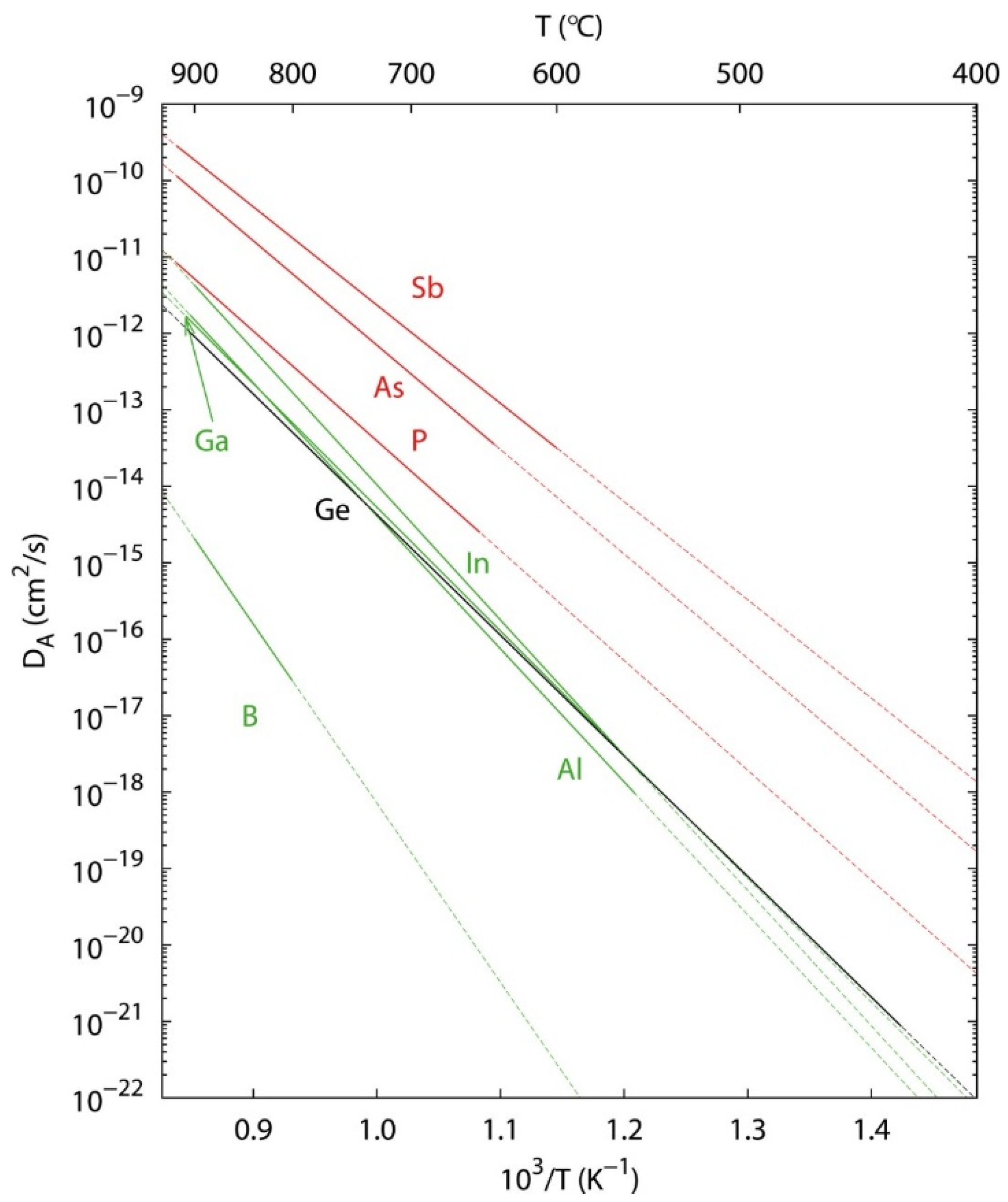
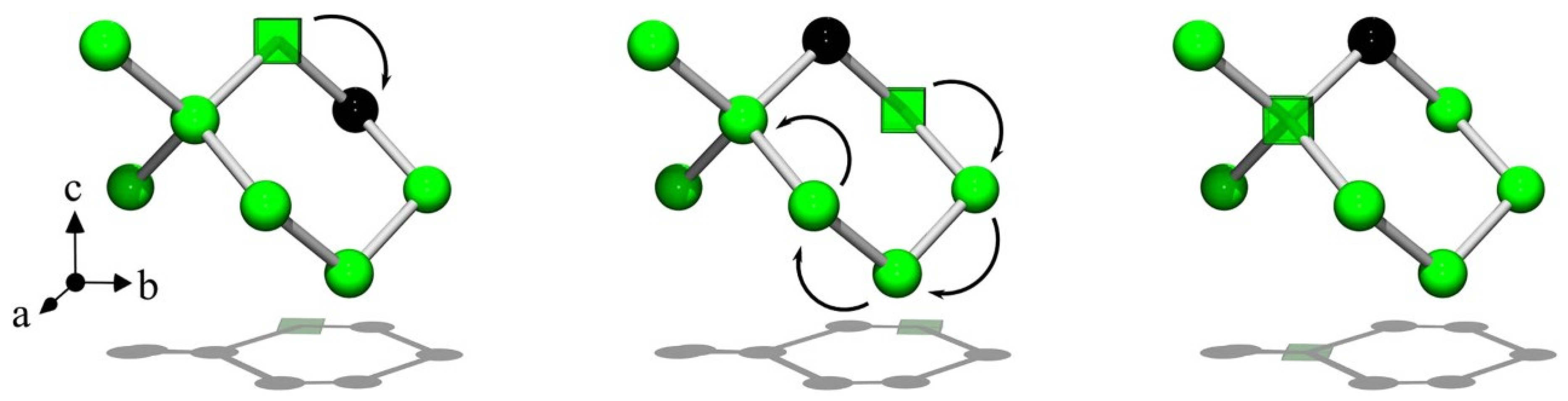
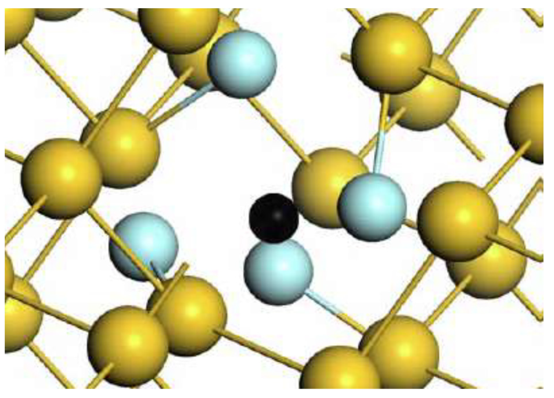
4.3. Acceptor Atoms
4.4. Carbon and Oxygen Impurities
5. Open Issues and Perspectives for the Future
6. Conclusions
Author Contributions
Funding
Institutional Review Board Statement
Informed Consent Statement
Conflicts of Interest
References
- Brattain, W. Bell Labs Logbook, December 1947. Available online: https://www.pbs.org/transistor/science/labpages/labpg1.html (accessed on 20 October 2022).
- Bardeen, J.; Brattain, W. The transistor, a semiconductor triode. Phys. Rev. 1948, 74, 230–231. [Google Scholar] [CrossRef]
- Riordan, M.; Hoddeson, L. Crystal Fire: The Birth of the Information Age; W. W. Norton: New York, NY, USA, 1997. [Google Scholar]
- Lilienfeld, J.E. Method and Apparatus for Controlling Electric Currents. U.S. Patent 1745175A, 8 October 1926. [Google Scholar]
- Bassett, R. To the Digital Age: Research Labs, Start-up Companies, and the Rise of MOS Technology; JHU Press: Baltimore, MD, USA, 2002; pp. 12–28. [Google Scholar]
- Moore, G.E. Cramming more components onto integrated circuits. Electronics 1965, 38, 114–118. [Google Scholar] [CrossRef]
- Burg, D.; Ausubel, J.H. Moore’s Law revisited through intel chip density. PLoS ONE 2021, 16, e0256245. [Google Scholar] [CrossRef]
- International Roadmap for Devices and Systems (IRDS), 2020 Edition, IEEE. Available online: https://irds.ieee.org/topics/semiconductors-and-artificial-intelligence (accessed on 20 October 2022).
- McKinsey and Company, Artificial Intelligence Hardware: New Opportunities for Semiconductor Companies, December 2018. Available online: https://www.mckinsey.com/~/media/McKinsey/Industries/Semiconductors/Our%20Insights/Artificial%20intelligence%20hardware%20New%20opportunities%20for%20semiconductor%20companies/Artificial-intelligence-hardware.ashx (accessed on 20 October 2022).
- Sistani, M.; Böckle, R.; Falkensteiner, D.; Luong, M.A.; den Hertog, M.I.; Lugstein, A.; Weber, W.M. Nanometer-scale Ge-based adaptable transistors providing programmable negative differential resistance enabling multivalued logic. ACS Nano 2021, 15, 18135–18141. [Google Scholar] [CrossRef] [PubMed]
- Werner, M.; Mehrer, H.; Hochheimer, H.D. Effect of hydrostatic pressure, temperature, and doping on self-diffusion in germanium. Phys. Rev. B 1985, 32, 3930–3937. [Google Scholar] [CrossRef]
- Stolwijk, N.A.; Bracht, H. Diffusion in Silicon, Germanium and Their Alloys; Landolt-Börnstein New Series; Subvolume A Springer: New York, NY, USA, 1998; Volume III/33. [Google Scholar]
- Cheng, B.H.; Cao, M.; Rao, R.; Inani, A.; Voorde, P.V.; Greene, W.M.; Stork, J.M.C.; Yu, Z.P.; Zeitzoff, P.M.; Woo, J.C.S. The impact of high-k gate dielectrics and metal gate electrodes on sub-100 nm MOSFET’s. IEEE Trans. Electron Dev. 1999, 46, 1537–1544. [Google Scholar] [CrossRef]
- Smith, R.C.; Ma, T.; Hoilien, N.; Tsung, L.Y.; Bevan, M.J.; Colombo, L.; Roberts, J.; Campbell, S.A.; Gladfelter, W.L. Chemical vapour deposition of the oxides of titanium, zirconium and hafnium for use as high-k materials in microelectronic devices. A carbon-free precursor for the synthesis of hafnium dioxide. Adv. Mater. Opt. Electron. 2000, 10, 105–114. [Google Scholar] [CrossRef]
- Ngai, T.; Qi, W.J.; Sharma, R.; Fretwell, J.; Chen, X.; Lee, J.C.; Benerjee, S. Electrical properties of ZrO2 gate dielectric on SiGe. Appl. Phys. Lett. 2000, 76, 502–504. [Google Scholar] [CrossRef]
- Frank, M.M.; Koester, S.J.; Copel, M.; Ott, J.A.; Paruchuri, V.K.; Shang, H.; Loesing, R. Hafnium oxide gate dielectrics on sulfur-passivated germanium. Appl. Phys. Lett. 2006, 89, 112905. [Google Scholar] [CrossRef]
- Saraswat, K.C.; Chui, C.O.; Krishnamohan, T.; Nayfeh, A.; McIntyre, P. Ge based high performance nanoscale MOSFETs. Microelectron. Eng. 2005, 80, 15–21. [Google Scholar] [CrossRef]
- Kamata, Y. High-k/Ge MOSFTETs for future nanoelectronics. Mater. Today 2008, 11, 30–38. [Google Scholar] [CrossRef]
- Chroneos, A.; Dimoulas, A. Defect configuration of high-k cations in germanium. J. Appl. Phys. 2012, 111, 023714. [Google Scholar] [CrossRef]
- Broqvist, P.; Binder, J.F.; Pasquarello, A. Formation of substoichiometric GeOx at the Ge-HfO2 interface. Appl. Phys. Lett. 2010, 97, 202908. [Google Scholar] [CrossRef]
- Chroneos, A.; Schwingenschlögl, U.; Dimoulas, A. Impurity diffusion, point defect engineering and surface/interface passivation in germanium. Ann. Phys. 2012, 524, 123–132. [Google Scholar] [CrossRef]
- Wu, M.L.; Wu, Y.H.; Chao, C.Y.; Lin, C.C.; Wu, C.Y. Crystalline ZrTiO4 gated Ge metal oxide semiconductor devices with amorphous Yb2O3 as a passivation layer. IEEE Trans. Nanotechnol. 2013, 12, 1018–1021. [Google Scholar] [CrossRef]
- Giese, A.; Stolwijk, N.A.; Bracht, H. Double-hump diffusion profiles of copper and nickel in germanium wafers yielding vacancy-related diffusion. Appl. Phys. Lett. 2000, 77, 642–644. [Google Scholar] [CrossRef]
- Da Silva, A.J.R.; Janotti, A.; Fazzio, A.; Baierle, R.J.; Mota, R. Self-interstitial defect in germanium. Phys. Rev. B 2000, 62, 9903–9906. [Google Scholar] [CrossRef]
- Coutinho, J.; Jones, R.; Briddon, P.R.; Öberg, S. Oxygen and dioxygen centers in Si and Ge: Density functional calculations. Phys. Rev. B 2000, 62, 10824. [Google Scholar] [CrossRef]
- Tsouroutas, P.; Tsoukalas, D.; Florakis, A.; Zergioti, I.; Serafetinides, A.A.; Cherkashin, N.N.; Marty, B.; Claverie, A. Laser annealing for n+/p junction formation in germanium. Mater. Sci. Semicond. Proc. 2006, 9, 644–649. [Google Scholar] [CrossRef]
- Bracht, H.; Brotzmann, S. Atomic transport in germanium and the mechanism of arsenic diffusion. Mater. Sci. Semicond. Proc. 2006, 9, 471–476. [Google Scholar] [CrossRef]
- Chroneos, A.; Skarlatos, D.; Tsamis, C.; Christofi, A.; McPhail, D.S.; Hung, R. Implantation an diffusion of phosphorous in germanium. Mater. Sci. Semicond. Proc. 2006, 9, 640–643. [Google Scholar] [CrossRef]
- Pinto, H.M.; Coutinho, J.; Torres, V.J.B.; Öberg, S.; Briddon, P.R. Formation energy and migration barrier of a Ge vacancy from ab initio studies. Mater. Sci. Semicond. Proc. 2006, 9, 498–502. [Google Scholar] [CrossRef]
- Silvestri, H.H.; Bracht, H.; Hansen, J.L.; Larsen, A.N.; Haller, E.E. Diffusion of silicon in crystalline germanium. Semicond. Sci. Technol. 2006, 21, 758–762. [Google Scholar] [CrossRef] [Green Version]
- Haller, E.E. Germanium: From its discovery to SiGe devices. Mater. Sci. Semicond. Proc. 2006, 9, 408–422. [Google Scholar] [CrossRef] [Green Version]
- Chroneos, A. Isovalent impurity-vacancy complexes in germanium. Phys. Status Solidi B 2007, 244, 3206–3210. [Google Scholar] [CrossRef]
- Claeys, C.; Simoen, E. Germanium-Based Technologies: From Materials to Devices; Elsevier: Amsterdam, The Netherlands, 2007. [Google Scholar]
- Vanhellemont, J.; Spiewak, P.; Sueoka, K. On the solubility and diffusivity of the intrinsic point defects in germanium. J. Appl. Phys. 2007, 101, 036103. [Google Scholar] [CrossRef]
- Chroneos, A.; Grimes, R.W.; Uberuaga, B.P.; Brotzmann, S.; Bracht, H. Vacancy-arsenic clusters in germanium. Appl. Phys. Lett. 2007, 91, 192106. [Google Scholar] [CrossRef]
- Schneider, S.; Bracht, H.; Petersen, M.C.; Lundsgaard Hansen, J.; Nylandsted Larsen, A. Proton irradiation of germanium isotope multilayer structures at elevated temperatures. J. Appl. Phys. 2008, 103, 033517. [Google Scholar] [CrossRef]
- Chroneos, A.; Bracht, H.; Grimes, R.W.; Uberuaga, B.P. Phosphorous clustering in germanium-rich silicon germanium. Mater. Sci. Eng. B 2008, 154–155, 72–75. [Google Scholar] [CrossRef]
- Naganawa, M.; Shimizu, Y.; Uematsu, M.; Itoh, K.M.; Sawano, K.; Shiraki, Y.; Haller, E.E. Charge states of vacancies in germanium investigated by simultaneous observation of germanium self-diffusion and arsenic diffusion. Appl. Phys. Lett. 2008, 93, 191905. [Google Scholar] [CrossRef]
- Janke, C.; Jones, R.; Coutinho, J.; Öberg, S.; Briddon, P.R. Ab initio investigation of phosphorus diffusion paths in germanium. Phys. Rev. B 2008, 77, 195210. [Google Scholar] [CrossRef]
- Chroneos, A.; Bracht, H.; Jiang, C.; Uberuaga, B.P.; Grimes, R.W. Nonlinear stability of E centers in Si1-xGex: Electronic structure calculations. Phys. Rev. B 2008, 78, 195201. [Google Scholar] [CrossRef] [Green Version]
- Hüger, E.; Tietze, U.; Lott, D.; Bracht, H.; Bougeard, D.; Haller, E.E.; Schmidt, H. Self-diffusion in germanium isotope multilayers at low temperatures. Appl. Phys. Lett. 2008, 93, 162104. [Google Scholar] [CrossRef] [Green Version]
- Brotzmann, S.; Bracht, H. Intrinsic and extrinsic diffusion of phosphorous, arsenic, and antimony in germanium. J. Appl. Phys. 2008, 103, 033508. [Google Scholar] [CrossRef]
- Chroneos, A.; Bracht, H.; Grimes, R.W.; Uberuaga, B.P. Vacancy-mediated dopant diffusion activation enthalpies for germanium. Appl. Phys. Lett. 2008, 92, 172103. [Google Scholar] [CrossRef] [Green Version]
- Brotzmann, S.; Bracht, H.; Lundsgaard Hansen, J.; Nylandsted Larsen, A.; Simoen, E.; Haller, E.E.; Christensen, J.S.; Werner, P. Diffusion and defect reactions between donors, C, and vacancies in Ge. I Experimental results. Phys. Rev. B 2008, 77, 235207. [Google Scholar] [CrossRef] [Green Version]
- Chroneos, A.; Grimes, R.W.; Uberuaga, B.P.; Bracht, H. Diffusion and defect reactions between donors, C, and vacancies in Ge. II Atomistic calculations of related complexes. Phys. Rev. B 2008, 77, 235208. [Google Scholar] [CrossRef]
- Kube, R.; Bracht, H.; Chroneos, A.; Posselt, M.; Schmidt, B. Intrinsic and extrinsic diffusion of indium in germanium. J. Appl. Phys. 2009, 106, 063534. [Google Scholar] [CrossRef] [Green Version]
- Chroneos, A. Effect of germanium substrate loss and nitrogen on dopant diffusion in germanium. J. Appl. Phys. 2009, 105, 056101. [Google Scholar] [CrossRef]
- Decoster, S.; De Vries, B.; Wahl, U.; Correia, J.G.; Vantomme, A. Lattice location study of implanted In in Ge. J. Appl. Phys. 2009, 105, 083522. [Google Scholar] [CrossRef]
- Chroneos, A.; Jiang, C.; Grimes, R.W.; Schwingenschlögl, U.; Bracht, H. Defect interactions in Sn1-xGex alloys. Appl. Phys. Lett. 2009, 94, 252104. [Google Scholar] [CrossRef] [Green Version]
- Chroneos, A.; Jiang, C.; Grimes, R.W.; Schwingenschlögl, U.; Bracht, H. E centers in Si1-x-yGexSny alloys. Appl. Phys. Lett. 2009, 95, 112101. [Google Scholar] [CrossRef] [Green Version]
- Bruno, E.; Mirabella, S.; Scapellato, G.; Impellizzeri, G.; Terrasi, A.; Priolo, F.; Napolitani, E.; De Salvador, D.; Mastramatteo, M.; Carnera, A. Mechanism of B diffusion in crystalline Ge under proton irradiation. Phys. Rev. B 2009, 80, 033204. [Google Scholar] [CrossRef]
- Chroneos, A.; Londos, C.A.; Bracht, H. A-centers and isovalent impurities in germanium: Density functional theory calculations. Mater. Sci. Eng. B 2011, 176, 453–457. [Google Scholar] [CrossRef]
- Chroneos, A. Dopant-vacancy cluster formation in germanium. J. Appl. Phys. 2010, 107, 076102. [Google Scholar] [CrossRef] [Green Version]
- Tahini, H.; Chroneos, A.; Grimes, R.W.; Schwingenschlögl, U. Diffusion of tin in germanium: A GGA+U approach. Appl. Phys. Lett. 2011, 99, 162103. [Google Scholar] [CrossRef] [Green Version]
- Pulikkotil, J.J.; Chroneos, A.; Schwingenschlögl, U. Structure of Sn1−xGex random alloys as obtained from the coherent potential approximation. J. Appl. Phys. 2011, 110, 036105. [Google Scholar] [CrossRef] [Green Version]
- Impellizzeri, G.; Boninelli, S.; Priolo, F.; Napolitani, E.; Spinella, C.; Chroneos, A.; Bracht, H. Fluorine effect on As diffusion in Ge. J. Appl. Phys. 2011, 109, 113527. [Google Scholar] [CrossRef]
- Stolwijk, N.A.; Lerner, L. Vacancy properties in germanium probed by cobalt diffusion. J. Appl. Phys. 2011, 110, 033526. [Google Scholar] [CrossRef]
- Tahini, H.; Chroneos, A.; Grimes, R.W.; Schwingenschlögl, U.; Dimoulas, A. Strain induced changes to the electronic structure of germanium. J. Phys. Condens. Matter 2012, 24, 195802. [Google Scholar] [CrossRef] [PubMed]
- Chroneos, A.; Bracht, H. Diffusion of n-type dopants in germanium. Appl. Phys. Rev. 2014, 1, 011301. [Google Scholar] [CrossRef] [Green Version]
- Chroneos, A.; Sgourou, E.N.; Londos, C.A.; Schwingenschlögl, U. Oxygen defect processes in silicon and silicon germanium. Appl. Phys. Rev. 2015, 2, 021306. [Google Scholar] [CrossRef] [Green Version]
- Simoen, E.; Schaekers, M.; Liu, J.B.; Luo, J.; Zhao, C.; Barla, K.; Collaert, N. Defect engineering for shallow n-type junctions in germanium: Facts and fiction. Phys. Status Solidi A 2016, 213, 2799–2808. [Google Scholar] [CrossRef]
- Chroneos, A.; Grimes, R.W.; Bracht, H.; Uberuaga, B.P. Engineering the free vacancy and active donor concentrations in phosphrous and arsenic double donor-doped germanium. J. Appl. Phys. 2008, 104, 113724. [Google Scholar] [CrossRef] [Green Version]
- Sigillito, A.J.; Tyryshkin, A.M.; Beeman, J.W.; Haller, E.E.; Itoh, K.M.; Lyon, S.A. Large stark tuning of donor electron spin qubits in germanium. Phys. Rev. B 2016, 94, 125204. [Google Scholar] [CrossRef] [Green Version]
- Kujala, J.; Sudkamp, T.; Slotte, J.; Makkonen, I.; Tuomisto, F.; Bracht, H. Vacancy-donor complexes in highly n-type Ge doped with As, P and Sb. J. Phys. Condens. Matter 2016, 28, 335801. [Google Scholar] [CrossRef]
- Saltas, V.; Chroneos, A.; Vallianatos, F.A. Composition and temperature dependence of self-diffusion in Si1-xGex alloys. Sci. Rep. 2017, 7, 1374. [Google Scholar] [CrossRef] [Green Version]
- Sgourou, E.N.; Panayiotatos, Y.; Vovk, R.V.; Chroneos, A. Toward defect engineering strategies to optimize energy and electronic materials. Appl. Sci. 2017, 7, 674. [Google Scholar] [CrossRef] [Green Version]
- Prussing, J.K.; Hamdana, G.; Bougeard, D.; Peiner, E.; Bracht, H. Quantitative scanning spreading resistance microscopy on n-type dopant diffusion profiles in germanium and the origin of dopant deactivation. J. Appl. Phys. 2019, 125, 085105. [Google Scholar] [CrossRef]
- Christopoulos, S.R.G.; Kuganathan, N.; Chroneos, A. Electronegativity and doping Si1-xGex alloys. Sci. Rep. 2020, 10, 7459. [Google Scholar] [CrossRef]
- Prucnal, S.; Liedke, M.O.; Wang, X.S.; Butterling, M.; Posselt, M.; Knoch, J.; Windgassen, H.; Hirschmann, E.; Berencen, Y.; Rebohle, L.; et al. Dissolution of donor-vacancy clusters in heavily doped n-type germanium. New J. Phys. 2020, 22, 123036. [Google Scholar] [CrossRef]
- Kipke, F.; Sudkamp, T.; Prussing, J.K.; Bougeard, D.; Bracht, H. Diffusion of boron in germanium at 800–900 °C revisited. J. Appl. Phys. 2020, 127, 025703. [Google Scholar] [CrossRef]
- Saputro, R.H.; Matsumura, R.; Fukata, N. Dopant redistribution in high-temperature-grown Sb-doped Ge epitaxial films. Cryst. Growth Des. 2021, 21, 6523–6528. [Google Scholar] [CrossRef]
- Kuganathan, N.; Bracht, H.; Davazoglou, K.; Kipke, F.; Chroneos, A. Impact of oxygen on gallium doped germanium. AIP Advances 2021, 11, 065122. [Google Scholar] [CrossRef]
- Igumbor, E.; Olaniyan, O.; Dongho-Nguimbo, G.M.; Mapasha, R.E.; Ahmad, S. Electronic properties and defect levels induced by n/p-type defect complexes in Ge. Mater. Sci. Semicond. Proc. 2022, 150, 106906. [Google Scholar] [CrossRef]
- Kuganathan, N.; Grimes, R.W.; Chroneos, A. Nitrogen-vacancy defects in germanium. AIP Adv. 2022, 12, 045110. [Google Scholar] [CrossRef]
- Chroneos, A.; Grimes, R.W.; Tsamis, C. Atomic scale simulations of arsenic-vacancy complexes in germanium and silicon. Mater. Sci. Semicond. Proc. 2006, 9, 536–540. [Google Scholar] [CrossRef]
- Letaw Jr, H.; Portnoy, W.M.; Slifkin, L. Self-diffusion in germanium. Phys. Rev. 1956, 102, 636–639. [Google Scholar] [CrossRef]
- Valenta, M.W.; Ramasastry, C. Effect of heavy doping on the self-diffusion of germanium. Phys. Rev. 1957, 106, 73–75. [Google Scholar] [CrossRef]
- Stolwijk, N.A.; Frank, W.; Hölzl, J.; Pearton, S.J.; Haller, E.E. Diffusion and solubility of copper in germanium. J. Appl. Phys. 1985, 57, 5211–5219. [Google Scholar] [CrossRef]
- Bracht, H.; Stolwijk, N.A.; Mehrer, H. Diffusion and solubility of copper, silver, and gold in germanium. Phys. Rev. B 1991, 43, 14465–14477. [Google Scholar] [CrossRef] [PubMed]
- Bracht, H. Copper related diffusion phenomena in germanium and silicon. Mater. Sci. Semicond. Proc. 2004, 7, 113–124. [Google Scholar] [CrossRef]
- Hu, S.M. On interaction potential, correlation factor, vacancy mobility, and activation energy of impurity diffusion in diamond lattice. Phys. Stat. Sol. (B) 1973, 60, 595–604. [Google Scholar] [CrossRef]
- Tahini, H.A.; Chroneos, A.; Grimes, R.W.; Schwingenschlögl, U.; Bracht, H. Point defect engineering strategies to retard phosphorous diffusion in germanium. Phys. Chem. Chem. Phys. 2013, 15, 367–371. [Google Scholar] [CrossRef] [PubMed]
- Chroneos, A.; Grimes, R.W.; Bracht, H. Fluorine cooping in germanium to suppress donor diffusion an093d deactivation. J. Appl. Phys. 2009, 106, 063707. [Google Scholar] [CrossRef] [Green Version]
- Jung, W.S.; Park, J.H.; Nainani, A.; Nam, D.; Saraswat, K.C. Fluorine passivation of vacancy defects in bulk germanium for Ge metal-oxide-semiconductor field-effect transistor application. Appl. Phys. Lett. 2012, 101, 072104. [Google Scholar] [CrossRef]
- Impellizzeri, G.; Napolitani, E.; Boninelli, S.; Sullivan, J.P.; Roberts, J.; Buckman, S.J.; Ruffell, S.; Priolo, F.; Privitera, V. Role of F on the electrical activation of As in Ge. ECS J. Solid State Sci. Technol. 2012, 1, Q44–Q46. [Google Scholar] [CrossRef]
- El Mubarek, H.A.W. Reduction of phosphorus diffusion in germanium by fluorine implantation. J. Appl. Phys. 2013, 114, 223512. [Google Scholar] [CrossRef]
- Liu, J.B.; Luo, J.; Simoen, E.; Niu, Y.X.; Yang, F.; Wang, G.L.; Wang, W.W.; Chen, D.P.; Li, J.F.; Zhao, C.; et al. Junction control by carbon and phosphorus co-implantation in pre-amorphized germanium. ECS J. Solid State Sci. Technol. 2016, 5, P315–P319. [Google Scholar] [CrossRef]
- Lopez, G.M.; Fiorentini, V.; Impellizzeri, G.; Mirabella, S.; Napolitani, E. Fluorine in Si: Native-defect complexes and the suppression of impurity diffusion. Phys. Rev. B 2005, 72, 045219. [Google Scholar] [CrossRef]
- Lopez, G.M.; Fiorentini, V. Large fluorine-vacancy clusters in Si and their capture efficiency for self-interstitials. Appl. Phys. Lett. 2006, 89, 092113. [Google Scholar] [CrossRef]
- Harrison, S.A.; Edgar, T.F.; Hwang, G.S. Prediction of the anomalous fluorine-silicon interstitial pair diffusion in crystalline silicon. Phys. Rev. B 2006, 74, 121201. [Google Scholar] [CrossRef]
- Kiga, R.; Uematsu, M.; Itoh, K.M. Effect of fluorine on the suppression of boron diffusion in pre-amorphized silicon. J. Appl. Phys. 2020, 128, 105701. [Google Scholar] [CrossRef]
- Sio, H.C.; Kang, D.; Liu, R.; Stuckelberger, J.; Samundsett, C.; Macdonald, D. Fluorine passivation of defects and interfaces in crystalline silicon. ACS Appl. Mater. Interfaces 2021, 13, 32503–32509. [Google Scholar] [CrossRef]
- Satta, A.; Simoen, E.; Clarysse, T.; Janssens, T.; Benedetti, A.; De Jaeger, B.; Meuris, M.; Vandervorst, W. Diffusion, activation, and recrystallization of boron implanted in preamorphized and crystalline germanium. Appl. Phys. Lett. 2005, 87, 172109. [Google Scholar] [CrossRef]
- Impellizzeri, G.; Mirabella, S.; Irrera, A.; Grimaldi, M.G.; Napolitani, E. Ga-implantation in Ge: Electrical activation and clustering. J. Appl. Phys. 2009, 106, 013518. [Google Scholar] [CrossRef]
- Bracht, H.; Schneider, S.; Klug, J.N.; Liao, C.Y.; Hansen, J.L.; Haller, E.E.; Larsen, A.N.; Bougeard, D.; Posselt, M.; Wundisch, C. Interstitial-mediated diffusion in germanium under proton irradiation. Phys. Rev. Lett. 2009, 103, 255501. [Google Scholar] [CrossRef] [Green Version]
- Schneider, S.; Bracht, H.; Klug, J.N.; Hansen, J.L.; Larsen, A.N.; Bougeard, D.; Haller, E.E. Radiation-enhanced self- and boron diffusion in germanium. Phys. Rev. B 2013, 87, 115202. [Google Scholar] [CrossRef] [Green Version]
- Mirabella, S.; De Salvador, D.; Napolitani, E.; Bruno, E.; Priolo, F. Mechanisms of boron diffusion in silicon and germanium. J. Appl. Phys. 2013, 113, 031101. [Google Scholar] [CrossRef]
- Milazzo, R.; Linser, M. Impelizzeri, G.; Scarpa, D.; Giarola, M.; Sanson, A.; Mariotto, G.; Andrighetto, A.; Carnera, A.; Napolitani, E. P-type doping of Ge by Al ion implantation and pulsed laser melting. Appl. Surf. Sci. 2020, 509, 145230. [Google Scholar] [CrossRef]
- Foster, N.D.; Miller, A.J.; Hutchins-Delgado, T.A.; Smyth, C.M.; Wanke, M.C.; Lu, Z.M.; Luhman, D.R. Thermal activation of low-density Ga implanted in Ge. Appl. Phys. Lett. 2022, 120, 201902. [Google Scholar] [CrossRef]
- Janke, C.; Jones, R.; Öberg, S.; Briddon, P.R. Ab initio investigation of boron diffusion paths in germanium. J. Mater. Sci. Mater. Electron. 2007, 18, 775–780. [Google Scholar] [CrossRef]
- Chroneos, A.; Kube, R.; Bracht, H.; Grimes, R.W.; Schwingenschlogl, U. Vacancy-indium clusters in implanted germanium. Chem. Phys. Lett. 2010, 490, 38–40. [Google Scholar] [CrossRef]
- Wang, G.J.; Mei, H.; Meng, X.H.; Mei, D.M.; Yang, G. The electrical properties and distribution of indium in germanium crystals. Mater. Sci. Semicond. Proc. 2018, 74, 342–346. [Google Scholar] [CrossRef]
- Corbett, J.W.; Watkins, G.D.; Mc Doland, R.S. New oxygen infrared bands in annealed irradiated silicon. Phys. Rev. 1964, 135, A1381–A1385. [Google Scholar] [CrossRef]
- Goesele, U.; Laveant, P.; Scholz, R.; Engler, N.; Werner, P. Diffusion engineering by carbon in Silicon, in Si Front-End Processing- Physics and Technology of Dopant-defect Interaction II. Mater. Res. Soc. Symp. Proc. 2000, 610, B7.1.1–B7.1.12. [Google Scholar]
- Chroneos, A.; Londos, C.A. Interaction of A-centers with isovalent impurities in silicon. J. Appl. Phys. 2010, 107, 093518. [Google Scholar] [CrossRef] [Green Version]
- Sgourou, E.N.; Timerkaeva, D.; Londos, C.A.; Aliprantis, D.; Chroneos, A.; Caliste, D.; Pochet, P. Impact of isovalent doping on the trapping of vacancy and interstitial related defects in Si. J. Appl. Phys. 2013, 113, 113506. [Google Scholar] [CrossRef] [Green Version]
- Murin, L.I.; Tolkacheva, E.A.; Lastovskii, S.B.; Markevich, V.P.; Mullins, J.; Peaker, A.R.; Svensson, B.G. Interaction of radiation-induced self-interstitials with vacancy-oxygen related defects VnO2 (n from 1 to 3) in silicon. Phys. Stat. Solidi A 2019, 216, 1800609. [Google Scholar] [CrossRef]
- Chroneos, A.; Londos, C.A.; Sgourou, E.N.; Pochet, P. Point defect engineering strategies to suppress A-center formation in silicon. Appl. Phys. Lett. 2011, 99, 241901. [Google Scholar] [CrossRef] [Green Version]
- Wang, H.; Chroneos, A.; Londos, C.A.; Sgourou, E.N.; Schwingenschlögl, U. A-centers in silicon studied with hybrid density functional theory. Appl. Phys. Lett. 2013, 103, 052101. [Google Scholar] [CrossRef]
- Wang, H.; Chroneos, A.; Sgourou, E.N.; Londos, C.A.; Schwingenschlogl, U. Carbon related defects in irradiated silicon revisited. Sci. Rep. 2014, 4, 4909. [Google Scholar] [CrossRef] [PubMed] [Green Version]
- Qin, Y.Z.; Wang, P.; Jin, S.J.; Cui, C.; Yang, D.R.; Yu, X.G. Effects of nitrogen doping on vacancy-oxygen complexes in neutron irradiated Czochralski silicon. Mater. Sci. Semicond. Proc. 2019, 98, 65–69. [Google Scholar] [CrossRef]
- Kras’ko, M.M.; Kolosiuk, A.G.; Neimash, V.B.; Povarchuk, V.Y.; Roguts’kyi, I.S.; Goushcha, A.O. Role of the intensity of high-temperature electron irradiation in accumulation of vacancy-oxygen defects in Cz n-Si. J. Mater. Res. 2021, 36, 1646–1656. [Google Scholar] [CrossRef]
- Pelenitsyn, V.; Korataev, P. First-principles study of radiation defects in silicon. Comp. Mater. Sci. 2022, 207, 111273. [Google Scholar] [CrossRef]
- Sueoka, K.; Kamiyama, E.; Spiewak, P.; Vanhellemont, J. Review—Properties of intrinsic point defects in Si and Ge assessed by density functional theory. ECS J. Solid State Sci. Technol. 2016, 5, P3176–P3195. [Google Scholar] [CrossRef]
- Chroneos, A.; Grimes, R.W.; Bracht, H. Impact of germanium on vacancy clustering in germanium-doped silicon. J. Appl. Phys. 2009, 105, 016102. [Google Scholar] [CrossRef]
- Rushton, M.J.D.; Chroneos, A.; Skinner, S.J.; Kilner, J.A.; Grimes, R.W. Effect of strain on the oxygen diffusion in yttria and gadolinia co-doped ceria. Solid State Ionics 2013, 230, 37–42. [Google Scholar] [CrossRef]
- Kelaidis, N.; Kordatos, A.; Christopoulos, S.R.G.; Chroneos, A. A roadmap of strain in doped anatase TiO2. Sci. Rep. 2018, 8, 12790. [Google Scholar] [CrossRef] [Green Version]
- Hussain, N.; Yao, Y.S.; Sagar, R.U.R.; Anwar, T.; Murtaza, M.; Huang, K.; Shehzad, K.; Wu, H.; Wang, Z.M. Quantum-confined blue photoemission in strain-engineered few-atomic-layer 2D germanium. Nano Energy 2021, 83, 105790. [Google Scholar] [CrossRef]
- Lee, M.L.; Fitzgerald, E.A. Strained Si, SiGe, and Ge channels for high-mobility metal-oxide-semiconductor field-effect transistors. J. Appl. Phys. 2005, 97, 011101. [Google Scholar] [CrossRef]
- Schichtel, N.; Korte, C.; Hesse, D.; Janek, J. Elastic strain at interfaces and its influence on ionic conductivity in nanoscaled solid electrolyte thin films- theoretical considerations and experimental studies. Phys. Chem. Chem. Phys. 2009, 11, 3043–3048. [Google Scholar] [CrossRef] [PubMed]
- Chiabrera, F.; Garbayo, I.; Lopez-Conesa, L.; Martin, G.; Ruiz-Caridad, A.; Walls, M.; Ruiz-Gonzalez, L.; Kordatos, A.; Nunez, M.; Morata, A.; et al. Engineering transport in manganites by tuning local nonstoichiometry in grain boundaries. Adv. Mater. 2019, 31, 1805360. [Google Scholar] [CrossRef] [PubMed] [Green Version]
- Baiutti, F.; Chiabrera, F.; Acosta, M.; Diercks, D.; Parfitt, D.; Santiso, J.; Wang, X.; Cavallaro, A.; Morata, A.; Wang, H.; et al. A high-entropy manganite in an ordered nanocomposite for long-term application in solid oxide cells. Nat. Commun. 2021, 12, 2660. [Google Scholar] [CrossRef]
- Kuganathan, N.; Baiutti, F.; Tarancon, A.; Fleig, J.; Chroneos, A. Defects energetics in the SrTiO3-LaCrO3 system. Solid State Ionics 2021, 361, 115570. [Google Scholar] [CrossRef]
- Varotsos, P. Calculation of the migration volume of vacancies in ionic solids from macroscopic parameters. Phys. Stat. Sol. (A) 1978, 47, K133–K136. [Google Scholar] [CrossRef]
- Varotsos, P.; Alexopoulos, K. Thermodynamics of Point Defects and Their Relation with the Bulk Properties; North-Holland: Amsterdam, The Netherlands, 1986. [Google Scholar]
- Varotsos, P. Comparison of models that interconnect point defect parameters in solids with bulk properties. J. Appl. Phys. 2007, 101, 123503. [Google Scholar] [CrossRef]
- Murphy, S.T.; Chroneos, A.; Jiang, C.; Schwingenschlögl, U.; Grimes, R.W. Deviations from Vegard’s law in ternary III-V alloys. Phys. Rev. B 2010, 82, 073201. [Google Scholar] [CrossRef] [Green Version]
- Murphy, S.T.; Chroneos, A.; Grimes, R.W.; Jiang, C.; Schwingenschlögl, U. Phase stability and the arsenic vacancy defect in InxGa1-xAs. Phys. Rev. B 2011, 84, 184108. [Google Scholar] [CrossRef] [Green Version]
- Chroneos, A.; Vovk, R.V. Modeling self-diffusion in UO2 and ThO2 by connecting point defect parameters with bulk properties. Solid State Ionics 2015, 274, 1–3. [Google Scholar] [CrossRef]
- Cooper, M.W.D.; Grimes, R.W.; Fitzpatrick, M.E.; Chroneos, A. Modeling oxygen self-diffusion in UO2 under pressure. Solid State Ionics 2015, 282, 26–30. [Google Scholar] [CrossRef]
- Chroneos, A. Connecting point defect parameters with bulk properties to describe diffusion in solids. Appl. Phys. Rev. 2016, 3, 041304. [Google Scholar] [CrossRef] [Green Version]
- Saltas, V.; Chroneos, A.; Vallianatos, F.A. A thermodynamic approach of self- and hetero-diffusion in GaAs: Connecting point defect parameters with bulk properties. RSC Adv. 2016, 6, 53324–53330. [Google Scholar] [CrossRef]
- Magomedov, M.N. Parameters of the vacancy formation and self-diffusion in iron. J. Phys. Chem. Solids 2023, 172, 111084. [Google Scholar] [CrossRef]
- Jing, Y.; Zhang, X.; Wu, D.H.; Zhao, X.D.; Zhou, Z. High carrier mobility and pronounced light absorption in methyl-terminated germanene: Insights from first-principles. J. Phys. Chem. Lett. 2015, 6, 4252–4258. [Google Scholar] [CrossRef] [PubMed]
- Zhu, J.J.; Chroneos, A.; Schwingenschlögl, U. Silicene/germanene on MgX2 (X = Cl, Br, and I) for Li-ion batteries. Nanoscale 2016, 8, 7272–7277. [Google Scholar] [CrossRef]
- Kovalska, E.; Antonatos, N.; Luxa, J.; Sofer, Z. Edge-hydrogenated germanene by electrochemical decalcification-exfoliation of CaGe2: Germanene-enabled vapor sensor. ACS Nano 2021, 15, 16709–16718. [Google Scholar] [CrossRef]
- Zhao, F.L.; Feng, Y.Y.; Feng, W. Germanium-based monoelemental and binary two-dimensional materials: Theoretical and experimental investigations and promising applications. Infomat 2022, 4, e12365. [Google Scholar] [CrossRef]
- Liu, R.Q.; Kumar, A.; Chen, Z.Z.; Agrawal, A.; Sundararaghavan, V.; Choudhary, A. A predictive machine learning approach for microstructure optimization and materials design. Sci. Rep. 2015, 5, 22552. [Google Scholar] [CrossRef] [Green Version]
- Jay, E.E.; Rushton, M.J.D.; Chroneos, A.; Grimes, R.W.; Kilner, J.A. Genetics of superionic conductivity in lithium lanthanum titanates. Phys. Chem. Chem. Phys. 2015, 17, 178–183. [Google Scholar] [CrossRef]
- Mathew, J.; Parfitt, D.; Wilford, K.; Riddle, N.; Alamaniotis, M.; Chroneos, A.; Fitzpatrick, M.E. Reactor pressure vessel embrittlement: Insights from neural network modelling. J. Nucl. Mater. 2018, 502, 311–322. [Google Scholar] [CrossRef]
- Gubernatis, J.E.; Lookman, T. Machine learning in materials design and discovery: Examples from the present and suggestions for the future. Phys. Rev. Mater. 2018, 2, 120301. [Google Scholar] [CrossRef]
- Mathew, J.; Griffin, J.; Alamaniotis, M.; Kanarachos, S.; Fitzpatrick, M.E. Prediction of welding residual stresses using machine learning: Comparison between neural networks and neuro-fuzzy systems. Appl. Soft Comp. 2018, 70, 131–146. [Google Scholar] [CrossRef]
- Scappucci, G.; Kloeffel, C.; Zwanenburg, F.A.; Loss, D.; Myronov, M.; Zhang, J.J.; De Franceschi, S.; Katsaros, G.; Veldhorst, M. The germanium quantum information route. Nat. Rev. Mater. 2021, 6, 926–943. [Google Scholar] [CrossRef]

Publisher’s Note: MDPI stays neutral with regard to jurisdictional claims in published maps and institutional affiliations. |
© 2022 by the authors. Licensee MDPI, Basel, Switzerland. This article is an open access article distributed under the terms and conditions of the Creative Commons Attribution (CC BY) license (https://creativecommons.org/licenses/by/4.0/).
Share and Cite
Sgourou, E.N.; Daskalopulu, A.; Tsoukalas, L.H.; Stamoulis, G.; Vovk, R.V.; Chroneos, A. Seventy-Five Years since the Point-Contact Transistor: Germanium Revisited. Appl. Sci. 2022, 12, 11993. https://doi.org/10.3390/app122311993
Sgourou EN, Daskalopulu A, Tsoukalas LH, Stamoulis G, Vovk RV, Chroneos A. Seventy-Five Years since the Point-Contact Transistor: Germanium Revisited. Applied Sciences. 2022; 12(23):11993. https://doi.org/10.3390/app122311993
Chicago/Turabian StyleSgourou, Efstratia N., Aspassia Daskalopulu, Lefteri H. Tsoukalas, George Stamoulis, Ruslan V. Vovk, and Alexander Chroneos. 2022. "Seventy-Five Years since the Point-Contact Transistor: Germanium Revisited" Applied Sciences 12, no. 23: 11993. https://doi.org/10.3390/app122311993
APA StyleSgourou, E. N., Daskalopulu, A., Tsoukalas, L. H., Stamoulis, G., Vovk, R. V., & Chroneos, A. (2022). Seventy-Five Years since the Point-Contact Transistor: Germanium Revisited. Applied Sciences, 12(23), 11993. https://doi.org/10.3390/app122311993