Article

Dual-Mode Control Scheme to Improve Light Load Efficiency for Dual Active Bridge DC-DC Converters Using Single-Phase-Shift Control

1
Department of Power Mechanical Engineering, National Formosa University, No. 64, Wunhua Rd., Huwei Township, Yunlin County 632, Taiwan
2
Department of Vehicle Engineering, National Formosa University, No. 64, Wunhua Rd., Huwei Township, Yunlin County 632, Taiwan
*
Author to whom correspondence should be addressed.
Appl. Sci. 2022, 12(23), 12356; https://doi.org/10.3390/app122312356
Submission received: 30 September 2022 / Revised: 26 November 2022 / Accepted: 1 December 2022 / Published: 2 December 2022

Abstract

:
In vehicle-to-grid (V2G) applications, dual active bridge (DAB) converters are commonly used as the power interface because they offer high efficiency, galvanic isolation, and bidirectional power flow. For the DAB control strategy, phase-shift control is the mainstream, especially the single-phase-shift (SPS) method because of its ease of implementation. However, due to the phase shift, a DAB converter operated under this control method has relatively high backflow power, resulting in poor efficiency. The SPS control method has the drawback of high backflow power, especially at light loads. Thus, this paper proposes a new dual-mode control scheme to improve the light load efficiency of DAB converters by taking advantage of the pulse-width modulation (PWM) strategy in combination with the conventional SPS strategy for DAB converters based on load conditions. In other words, when the DAB converter operates under light load conditions, the PWM control strategy is used to avoid considerable backflow power. A prototype DAB converter with a power rating of 1 kW under a switching frequency of 100 kHz interfacing a DC bus (400 V) and a battery pack (50 V) is designed and implemented to verify the feasibility of this control strategy. A detailed analysis of the working principle and design parameters of the proposed converter is provided in this paper. Experimental results show that the highest efficiency of the proposed converter at light loads (10–200 W) was 96.2% for the forward power conversion and 97.3% for the backward power conversion.

1. Introduction

Nowadays, countries around the world are constantly seeking ways to utilize energy efficiently and reduce environmental impacts associated with carbon emissions. One of the most popular solutions today is using the smart grid, which provides a sustainable, reliable, economical, and environmentally friendly power grid [1]. The ability to connect electric vehicles (EVs) to the grid is one of the key features of a smart grid, which reduces emissions and fossil energy consumption. In a smart grid, Evs can be regarded as mobile energy storage. By connecting Evs to the grid, the overall energy utilization rate can be improved.
Since power electronics technology has evolved rapidly in recent years, DC/DC converters have been widely used in Evs, energy storage systems, energy conversion systems, DC distributed power systems, and power transmission systems. Moreover, DC-DC converters even appear in applications such as inverters [2]. One of the most popular topologies used in the DC/DC converter is the dual active bridge (DAB). Due to the attractive characteristics such as zero-voltage switching (ZVS) of all power switches, near-minimal voltage and current stress, galvanic isolation with bidirectional power flow, low number of passive components as well as a high voltage conversion ratio [3,4,5,6,7,8,9], the DAB converter is widely used as the power interface for Evs in V2G systems. A DAB converter topology typically consists of a high-frequency transformer and two active full-bridge rectifiers, as shown in Figure 1. The DAB converter has bidirectional energy transmission characteristics, and it is commonly controlled by phase-shift control to change its transferred power.
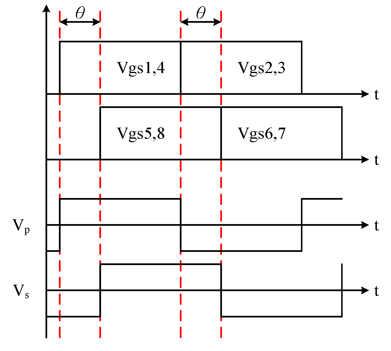
There are numerous phase-shift control methods applied to DAB converters. Generally, they can be categorized as SPS control, extended-phase-shift (EPS) control, dual-phase-shift (DPS) control, and triple-phase-shift (TPS) control. Among these control methods, the SPS control method is the most widely used due to its advantages, such as ease of implementation, simple algorithms used, soft switching capabilities, etc. In the SPS control method, diagonally opposite switches on each full-bridge are controlled to create a leading or lagging phase of the primary side voltage relative to the secondary side voltage of the transformer to control power flow direction and magnitude. The phase difference between the voltages on the primary side VP and the secondary side VS, the so-called phase-shift angle, θ, is the only variable that can be controlled, as shown in Figure 2.
When the control signal of the full-bridge rectifier on the primary side of the transformer is ahead of the control signal of the full-bridge rectifier on the secondary side of the transformer, the energy is transferred from the DC bus to the energy storage (battery pack). Conversely, when the control signal of the full-bridge rectifier on the secondary side of the transformer precedes that of the full-bridge rectifier on the primary side of the transformer, energy is transferred from the energy storage to the DC bus. With the aim of achieving ZVS for power switches, auxiliary inductor LK serves as a means of transferring and storing energy.
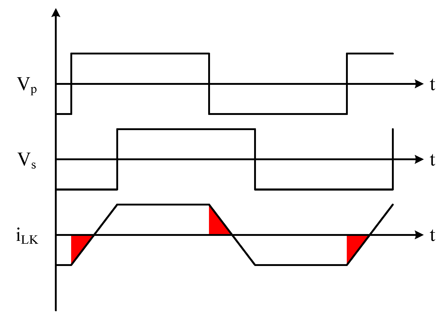
However, the disadvantage of SPS is the occurrence of backflow power caused by the circulating current. There are periods during the power transfer process when the transformer’s primary side voltage VP and inductor current iLK are in opposing directions, causing the energy stored in auxiliary inductor LK to return to the input (DC bus), as the red area in Figure 3. As the transmission power remains constant, the greater the backflow power, the greater the required forward transmission power. The backflow power also leads to higher current stress on the power switches, causing an increase in conduction loss and the magnetic loss of the transformer, resulting in lower converter efficiency, especially at light loads.
For better efficiency of DAB converters at light load, several control strategies were developed, such as EPS control [10,11] or series resonant dual-active bridge (SRDAB) converters [12,13]. EPS control can effectively reduce the current stress and reactive power and thus increase the system efficiency, but the phase-shift degrees of freedom also increase. This control method adds another degree of freedom to the converter by adjusting the time sequence between the gate signals of diagonal power switches to enhance flexibility. Ref. [10] proposed a minimum-backflow-power under extended-phase-shift control (MEPS) strategy to minimize the backflow power and improve the efficiency in a wide operating range. Ref. [11] presented a three-degree-of-freedom control method for DAB converters to achieve full load range ZVS under a wide voltage range. However, in practice, control complexity is high because of the number of coupled variables, making it difficult to implement. In terms of resonant converters, Ref. [12] introduced a symmetrical CLLC resonant tank on the DAB with pulse frequency modulation (PFM) control to achieve soft switching during bidirectional power conversion. In [13], a dual-bridge series resonant DC-DC converter (DBSRC) developed by modifying the topology of the traditional DBSRC was introduced. The proposed circuit presents higher voltage gain, a wider soft-switching region, and larger output power than the traditional DBSRC. However, the resonant converter commonly uses variable frequency control methods, which generate higher harmonics. As a result, the converter requires the use of more complex designed EMI suppression filters. To improve efficiency at light loads while taking advantage of the large power transmission capacity of SPS control, a fixed-frequency dual-mode control strategy is proposed in this paper, enabling the DAB converter to switch the operation mode based on the load. For example, the DAB converter operating at light loads is controlled by using PWM control. Nevertheless, when the converter is under medium-to-full load, the DAB converter is controlled by using the SPS control. Table 1 shows a comparison of the related studies.
This paper is structured as follows:
Section 1 introduces the DAB converter topology and its control strategies. This section also briefly mentions the purpose of this study and the paper structure. Section 2 describes the operation of the dual-mode control strategy for the DAB converter, along with its related circuit analysis. Section 3 presents the design procedure of the prototype converter. Section 4 establishes the power loss model of the converter. In Section 5, the experimental results prove the feasibility of the proposed dual-mode control strategy for the DAB converter. Moreover, the experimental data show that the light load efficiency of the proposed control strategy is higher than that of the traditional SPS control strategy. Section 6 concludes the paper.

2. Operating Principle of the Proposed Dual-Mode Control Strategy for the DAB Converter

The operating principle of the proposed dual-mode control strategy for the DAB converter breaks down into two parts: light load and medium-to-full load.
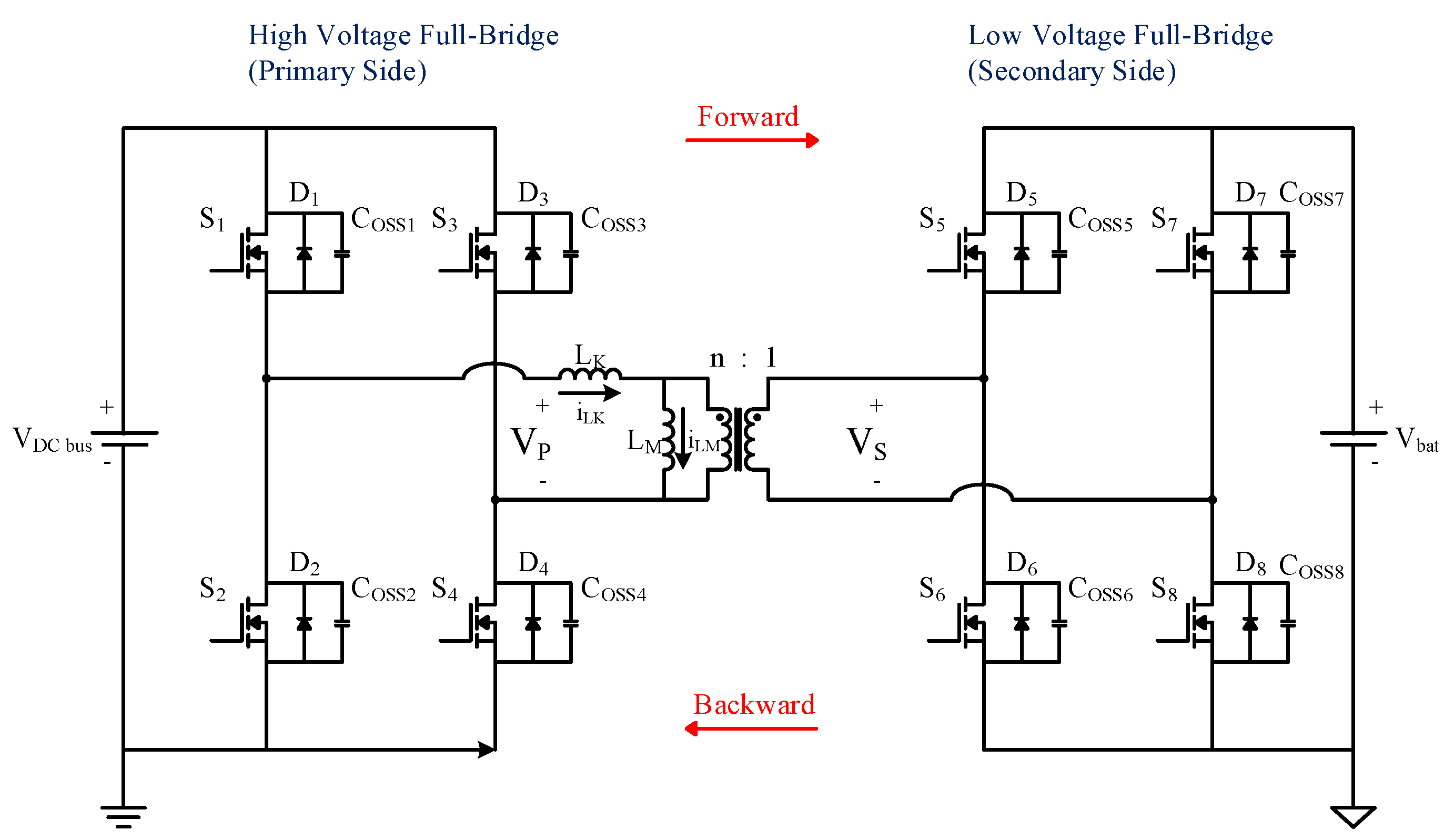
Since forward power conversion and backward power conversion operate similarly, the analysis will focus on the forward power conversion (power transferred from the DC bus to the battery pack). Figure 4 depicts the structure of the DAB converter for analysis. The components are defined as follows:
1. S1, S2, S3, and S4 are power switches of the high voltage full-bridge.
2. S5, S6, S7, and S8 are power switches of the low voltage full-bridge.
3. D1, D2, D3, and D4 are the intrinsic diodes of power switches S1, S2, S3, and S4 of the high voltage full-bridge, respectively.
4. D5, D6, D7, and D8 are the intrinsic diodes of power switches S5, S6, S7, and S8 of the low voltage full-bridge, respectively.
5. COSS1, COSS2, COSS3, and COSS4 are the parasitic capacitances of power switches S1, S2, S3, and S4 of the high voltage full-bridge, respectively.
6. COSS5, COSS6, COSS7, and COSS8 are the parasitic capacitances of power switches S5, S6, S7, and S8 of the low voltage full-bridge, respectively.
7. LM is the magnetizing inductance of the transformer.
8. LK is the sum of transformer leakage inductance and auxiliary inductance.
11. VDcbus is the voltage of the DC bus (high-voltage side).
12. Vbat is the voltage of the battery pack (low-voltage side).

2.1. Light Load

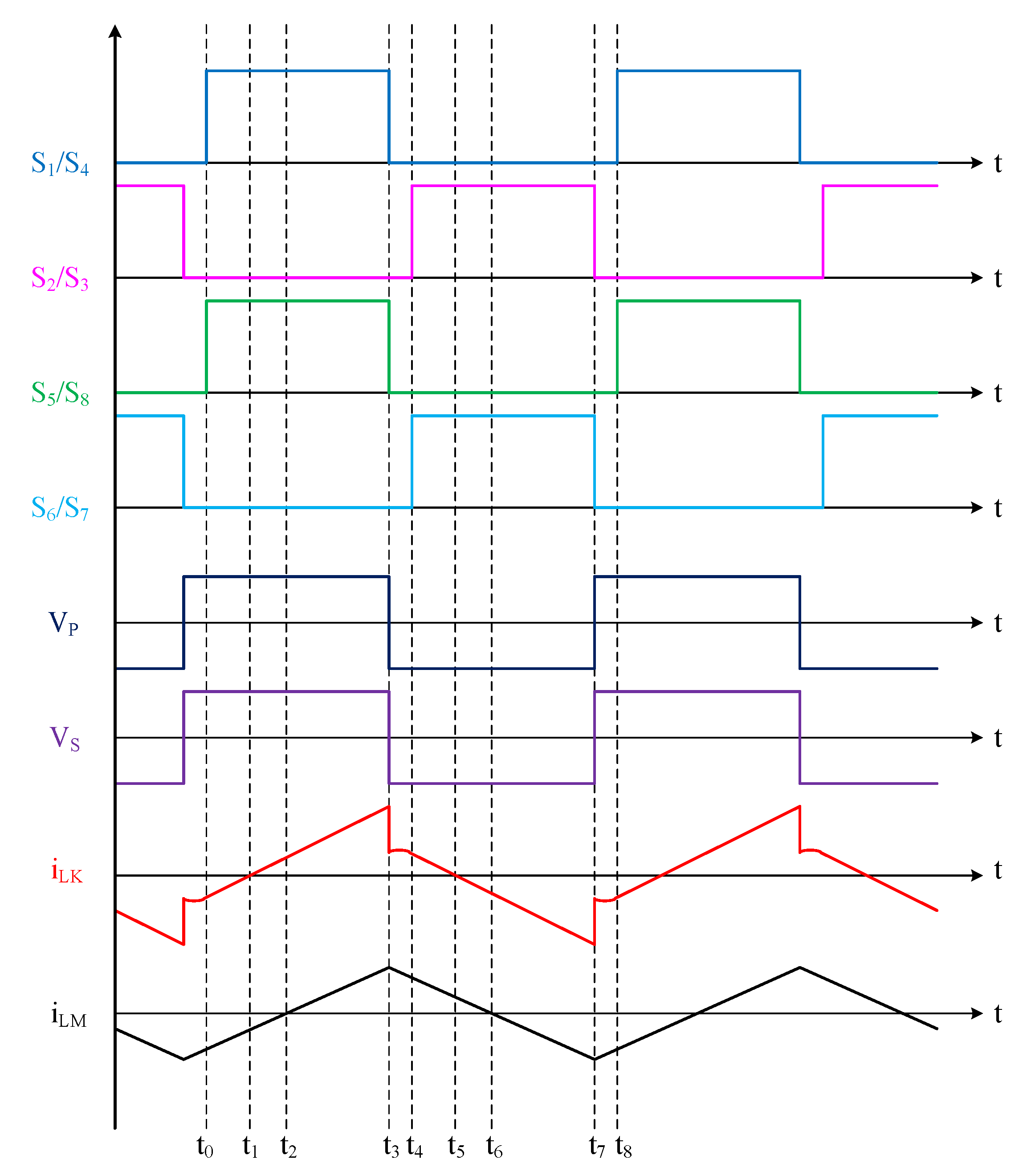
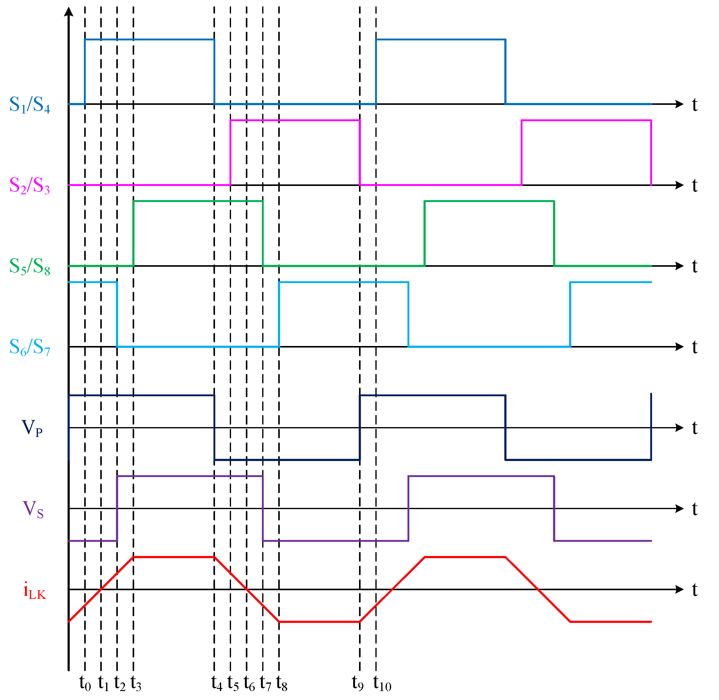
Under light load conditions, the proposed DAB converter adopts the PWM control to drive two full-bridges, which lowers the loss of backflow power and improves the efficiency of the DAB converter. Figure 5 demonstrates the theoretical waveforms of the proposed control strategy for the DAB converter in PWM mode under light load conditions.
State 1 (t0 ≤ t ≤ t1):
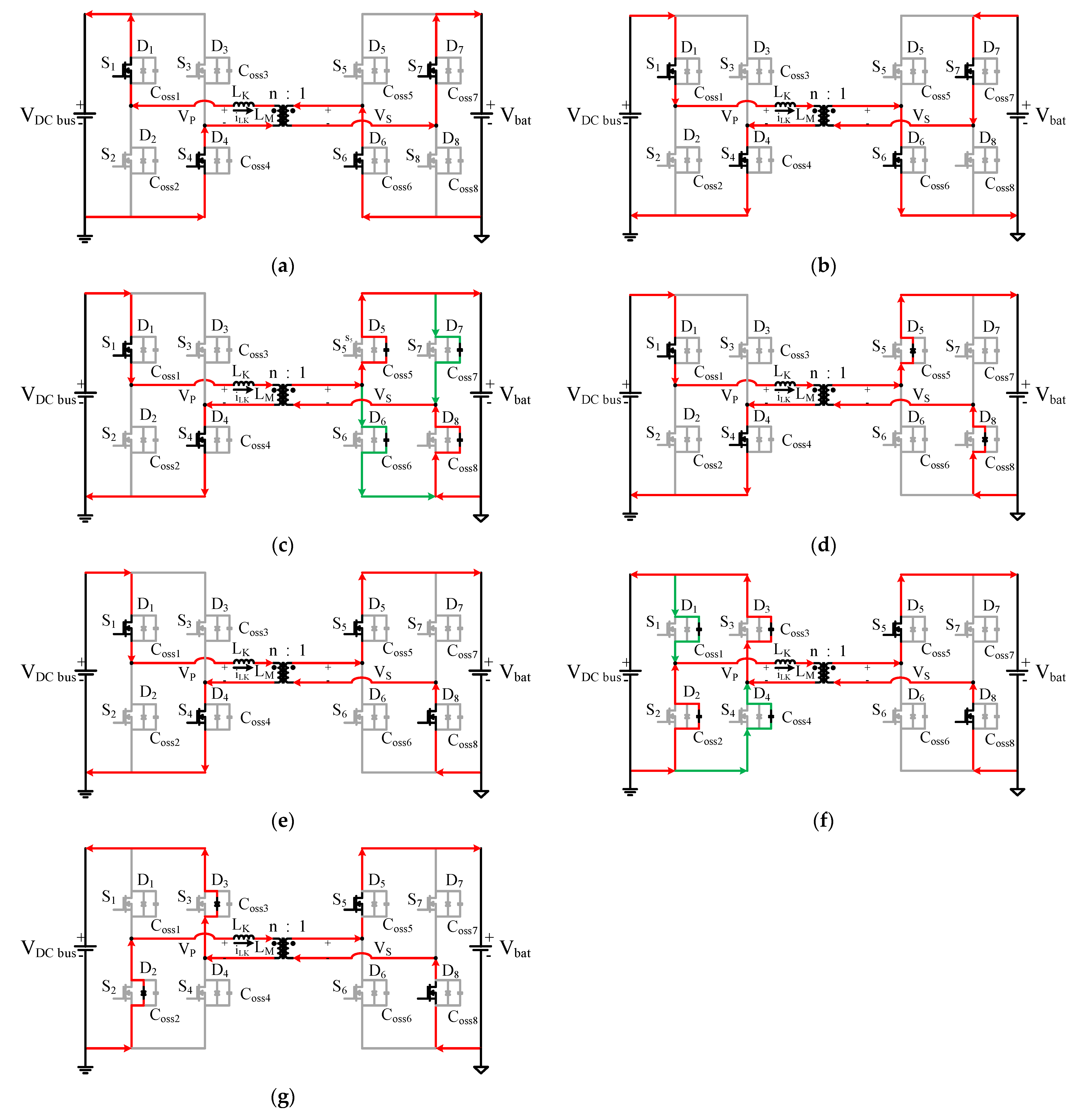
As shown in Figure 5, due to the discharge of energy stored in COSS1, COSS4, COSS5, and COSS8 to zero during the dead time in the previous state, switches S1, S4, S5, and S8 are turned on with ZVS at t = t0. Since LM and LK have not discharged their stored energy completely, currents iLM and iLK keep flowing in the same direction as their previous state until their stored energy is discharged to zero. The detailed current path is shown in Figure 6a.
State 2 (t1t ≤ t2):
As shown in Figure 5, at t = t1, switches S1, S4, S5, and S8 remain on. The energy stored in LK has been discharged to zero, causing LK to change its state from discharging to charging. Nevertheless, the energy stored in LM has not been discharged to zero. In this case, VDCbus will charge LK and combine with the LM, transferring the energy to the low-voltage side to provide the load. The detailed current path is shown in Figure 6b.
State 3 (t2tt3):
As shown in Figure 5, at t = t2, switches S1, S4, S5, and S8 remain on. At this time, LM has discharged its stored energy to zero, thus transitioning from discharge to charge energy. VDcbus charges inductors LM and LK, as well as supplies energy to the load. The detailed current path is shown in Figure 6c.
State 4 (t3 ≤ t ≤ t4):
At t = t3, switches S1, S4, S5, and S8 are turned off. The period from t3 to t4 is the dead time of the high- and low-voltage side switches. At this time, currents iLM and iLK flow in the same direction. The high-voltage side current discharges COSS2 and COSS3 to charge COSS1 and COSS4, combining with LM to transfer energy to the low-voltage side. The low-voltage side current discharges COSS6 and COSS7, charging COSS5 and COSS8, and providing energy to the load. The detailed current path is shown in Figure 6d.
Note that after the energy stored in COSS2, COSS3, COSS6, and COSS7 has been discharged to zero, intrinsic diodes D2, D3, D6, and D7 conduct the current during the remainder of this state. The detailed current path is shown in Figure 6e.
State 5 (t4 ≤ t ≤ t5):
As shown in Figure 5, due to the discharge of energy stored in COSS2, COSS3, COSS6, and COSS7 to zero during the dead time in state 4, switches S2, S3, S6, and S7 are turned on with ZVS at t = t4. Since LM and LK have not discharged their stored energy completely, currents iLM and iLK keep flowing in the same direction as their previous state until their stored energy is discharged to zero. The detailed current path is shown in Figure 6f.
States 6 to 8 work the same way as states 2 to 4; the only difference is that switches S2, S3, S6, and S7 take the place of switches S1, S4, S5, and S8. Therefore, there will be no further explanation.

2.2. Medium-to-Full Load

As the load condition changes from light load to medium-to-full load, the SPS control is used to operate the DAB converter, controlling the direction and magnitude of the transferred power. Figure 7 demonstrates the theoretical waveforms of the proposed control strategy for the DAB converter in SPS mode under medium-to-full load conditions.
State 1 (t0 ≤ t ≤ t1):
As shown in Figure 7, due to the discharge of energy stored in COSS1 and COSS4 to zero during the dead time in the previous state, switches S1 and S4 are turned on with ZVS at t = t0. Since inductor LK has not discharged its stored energy completely, current iLK keeps flowing in the same direction as that in the previous state until the energy stored in LK is discharged to zero. The detailed current path is shown in Figure 8a.
State 2 (t1 ≤ t ≤ t2):
As shown in Figure 7, at t = t1, switches S1, S4, S6, and S7 remain on. The energy stored in LK has been discharged to zero, causing LK to change its state from discharging to charging. At this time, VDCbus charges LK. Therefore, current iLK changes its direction and increases linearly. The detailed current path is shown in Figure 8b.
State 3 (t2 ≤ t ≤ t3):
As shown in Figure 7, at t = t2, switches S1 and S4 remain on, switches S6 and S7 are turned off. The period from t2 to t3 is the dead time of the low-voltage side switches. At this time, the low-voltage side current discharges COSS5 and COSS8, charging COSS6 and COSS7, and providing energy to the load. The detailed current path is shown in Figure 8c.
Note that after the energy stored in COSS5 and COSS8 has been discharged to zero, intrinsic diodes D5 and D8 conduct the current during the remainder of this state. The detailed current path is shown in Figure 8d.
State 4 (t3 ≤ t ≤ t4):
As shown in Figure 7, switches S1 and S4 remain on. Due to the discharge of energy stored in COSS5 and COSS8 to zero during the dead time in the previous state, switches S5 and S8 are turned on with ZVS at t = t3. The detailed current path is shown in Figure 8e.
State 5 (t4 ≤ t ≤ t5):
As shown in Figure 7, at t = t4, switches S5 and S8 remain on, while switches S1 and S4 are turned off. The period from t4 to t5 is the dead time of the high-voltage side switches. At this time, the high-voltage side current discharges COSS2 and COSS3, charging COSS1 and COSS4 and transferring energy to the low-voltage side to provide the load, and then flows back to VDcbus. The detailed current path is shown in Figure 8f.
Note that switches S5 and S8 remain on in this state. After the energy stored in COSS2 and COSS3 has been discharged to zero, intrinsic diodes D2 and D3 conduct the current. The detailed current path is shown in Figure 8g.
States 6 to 10 operate similarly to states 1 to 5, but there are some notable points as follows:
Switches S2, S3, S5, and S8 in state 6 and state 7 operate the same way as switches S1, S4, S6, and S7 in state 1 and state 2.
Switches S2, S3, S6, and S7 in states 7, 8, 9, and 10 operate the same way as switches S1, S4, S5, and S8 in states 2, 3, 4, and 5.
Therefore, there will be no further explanation.

3. Design of the DAB Converter Prototype

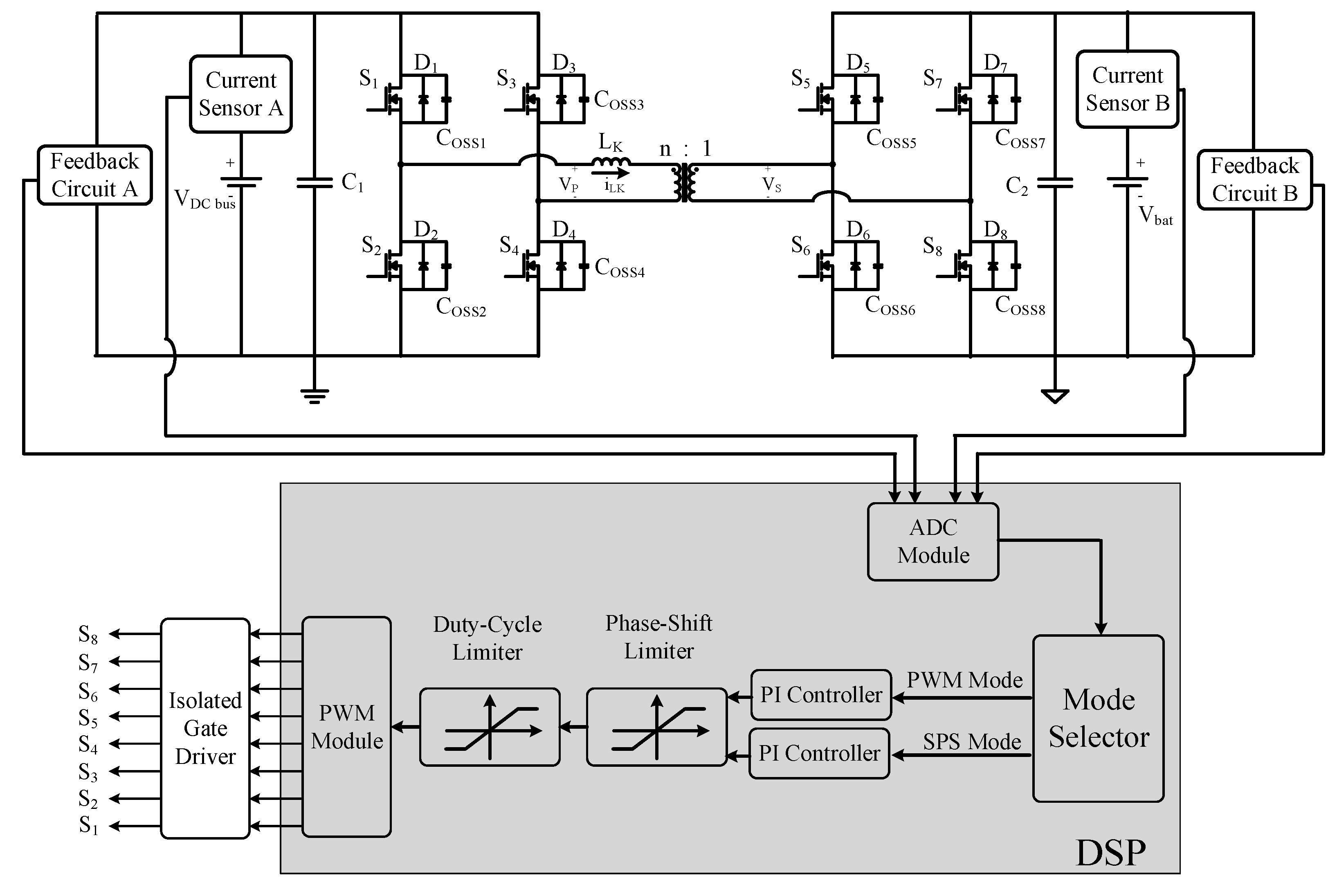
This paper employs a digital signal processor (DSP) to process the feedback signal from feedback circuits and control the mode switching, as shown in Figure 9.
The DSP program updates its input regularly by sampling the output voltage and current via the ADC module. These values serve to calculate the output power PO. The DSP program compares the PO value with a threshold value (200 W for forward conversion or 100 W for backward conversion) for mode switching. Based on the comparison result, the mode selector function will choose the suitable operation mode. A duty-cycle value or phase-shift value is calculated and sent to the PWM module, depending on the mode selected. There are two cases: when the energy is transferred from the VDcbus to Vbat, Vbat would be an output voltage. In this case, the voltage value from feedback circuit B and the current value from current sensor B will be used to calculate output power PO. On the other hand, when energy is transferred from Vbat to the VDcbus, the voltage value from feedback circuit A and the current value from current sensor A will be used to calculate output power PO.
The DAB converter prototype was designed in accordance with the design parameters in Table 2.
The rated power is 1 kW. The voltage of the high-voltage side is 400 V, and that of the low-voltage side is 50 V. For the high-voltage side of the converter, MOSFET SCT3080ALGC11, produced by ROHM Semiconductor (Kyoto, Japan), was selected for the power switch. On the other hand, MOSFET IRFP4321PBF, produced by Infineon (Neubiberg, Germany), was chosen for the power switches on the low-voltage side.
The flow chart diagram of the design process for energy storage components is given in Figure 10.

3.1. Transformer Selection

In order to achieve bidirectional power transfer, the DC bus voltage and the battery voltage are used as design criteria. Formula (1) is used to obtain the turns ratio.
n = N P N S = V D C b u s V b a t = 8
The transformer part number PC95PQ50/50Z-12, produced by TDK (Tokyo, Japan), is used as the high-frequency transformer of the proposed DAB prototype. The core is MnZn PC 95 ferrite core, and the coil former is PQ 50/50. According to the specifications provided by TDK, the effective cross-sectional area of the core is Ae = 3.28 cm2. By using the temperature characteristics curve of the transformer, it can be known that the saturation magnetic flux density of the iron core is about 410 mT at the temperature of 100 °C. To avoid the saturation of the transformer core, the maximum magnetic flux density Bmax is designed to be 0.31 times the saturation value, that is, 127 mT to ensure the normal operation of the transformer [14,15]. Since the transformer voltage is the square wave, the form factor Kf is 4. Finally, Formulas (2) and (3) are used to obtain the number of turns required for the high-voltage side winding, NP is 24 turns, and for the low-voltage side winding, NS is 3 turns.
N p = V D C b u s × 10 4 B m a x × K f × A e × f s w 24   turns
N s = N p n 3   turns

3.2. Inductor Selection

Formula (4) shows that the phase-shift ratio D varies with the maximum power transfer PMax of the DAB converter [16].
P M a x = D 1 D n × V D C b u s × V b a t f s w × L K
Therefore, it is necessary to take the phase-shift ratio value into account in the design of the inductor. Operating at the maximum power transfer point (D = 0.5) can maximize the ZVS range. However, the DAB converter operating at this value increases the backflow power loss. Thus, this paper chooses a phase-shift ratio of 0.2.
This phase-shift ratio value is substituted into Formula (4) and then rewritten as Formula (5). The proposed DAB prototype is designed with maximum power is 4.5 times its rated power. Substitute all parameters into Formula (5) to obtain the inductance value.
L K = 0.16 × n × V D C b u s × V b a t f s w × P M a x 57 μ H

3.3. Output Capacitor Selection

Output capacitors are commonly used to regulate and filter output voltage output. Equivalent series resistance (ESR) inside the capacitor affects the output voltage ripple. Increasing the RMS value of the capacitor current leads to more loss dissipated across the ESR of capacitance. Taking these factors into account, the output capacitor was selected to keep the ripple voltage below 5% as a design requirement. This paper calculates the capacitance of capacitors C1 and C2, respectively, using Formula 6 and Formula 7 [16], where the ripple of the VDcbusVDcbus) is 6 V, and the ripple of VbatVbat) is 0.75 V.
C 1 = P D C b u s 2 × f s w × V D C b u s × Δ V D C b u s 2.0833   μ F
C 2 = P b a t 2 × f s w × V b a t × Δ V b a t 133.3333   μ F
Considering the non-ideal case and the requirement for bidirectional power conversion, one 100 μF/450 V capacitor was chosen for the high-voltage side, and three 120 μF/63 V capacitors in parallel were selected for the low-voltage side.

4. Power Loss Model of the DAB Converter

Efficiency is related to transferred power and power losses. By taking into account the power switch losses, transformer losses, and inductor losses, a power loss model was built to verify the practical measured power efficiency.

4.1. Power Switch Losses

In this paper, the power switch is considered the ideal switch. Therefore, the power losses of the intrinsic diode can be ignored. Generally, power switch losses are divided into switching and conduction losses [17]. Switching loss, which is duty-cycle dependent, occurs during the turning on and turning off time of the power switch. Steady-state losses caused by a power switch can be calculated as follows:
The turn-on loss can be described as:
P S W o n = V D S × I P × T r × f s w 6
where VDS, IP, Tr refer to the drain voltage, peak current, and rising time of the power switch, respectively.
The turn-off loss can be described as:
P S W o f f = V D S × I P × T f × f s w 6
where Tf refers to the falling time of the power switch.
The switching losses can be expressed as:
P S W _ l o s s = P S W o n + P S W o f f
The gate drive loss can be calculated by using Formula (11).
P G a t e = C i s s + C r s s × V G S 2 2 × T
where Ciss, and Crss refer to the input capacitance and reverse transfer capacitance of the power switch, respectively. VGS is the gate-source voltage of the switch, and T is the switching period.
The conduction loss of the power switch can be calculated by using Formula (12).
P C o n d = I r m s 2 × R D S o n
where Irms refers to the RMS drain current, and RDS(on) is the conduction resistance.
The total power losses of the power switch can be expressed as Formula (13).
P L o s s S W = P S W _ l o s s + P G a t e + P C o n d

4.2. Transformer Losses

The transformer losses consist of copper losses and core losses. The core loss can be calculated by using Formula (14).
P C o r e l o s s T r = P C V T r × V e T r
where PCV(Tr) refers to the core loss density, and Ve(Tr) refers to the effective core volume of the transformer, respectively.
The copper loss of the transformer can be calculated as Formula (15).
P C o p p e r l o s s T r = I r m s P r i 2 × R C o p p e r P r i + I r m s S e c 2 × R C o p p e r S e c
where Irms(Pri), and Irms(Sec) refer to the RMS value of the primary side and secondary side current, respectively. RCopper(Pri), and RCopper(Sec) refer to the resistance of the primary side and secondary side winding, respectively.
The total power losses of the transformer can be expressed as Formula (16).
P L o s s T r = P C o r e l o s s T r + P C o p p e r l o s s T r

4.3. Inductor Losses

Similarly to transformers, the inductor power losses consist of copper losses and core losses. The core loss can be calculated by using Formula (17).
P C o r e l o s s I n = P C V I n × V e I n
where PCV(In) refers to the core loss density, and Ve(In) refers to the effective core volume of the inductor, respectively.
The copper loss of the inductor can be calculated as Formula (18).
P C o p p e r l o s s I n = I r m s I n 2 × R C o p p e r I n
where Irms(In) represents the RMS value of inductor current, and RCopper(In) represents the inductor winding resistance.
The total power losses of the inductor can be expressed as Formula (19).
P L o s s I n = P C o r e l o s s I n + P C o p p e r l o s s I n

4.4. Total Power Losses

Total power losses of the converter can be considered as the sum of switch losses, transformer losses, and inductor losses. Total power losses can be derived as follows:
P L o s s _ T o t a l = P L o s s S W + P L o s s T r + P L o s s I n

5. Experimental Results

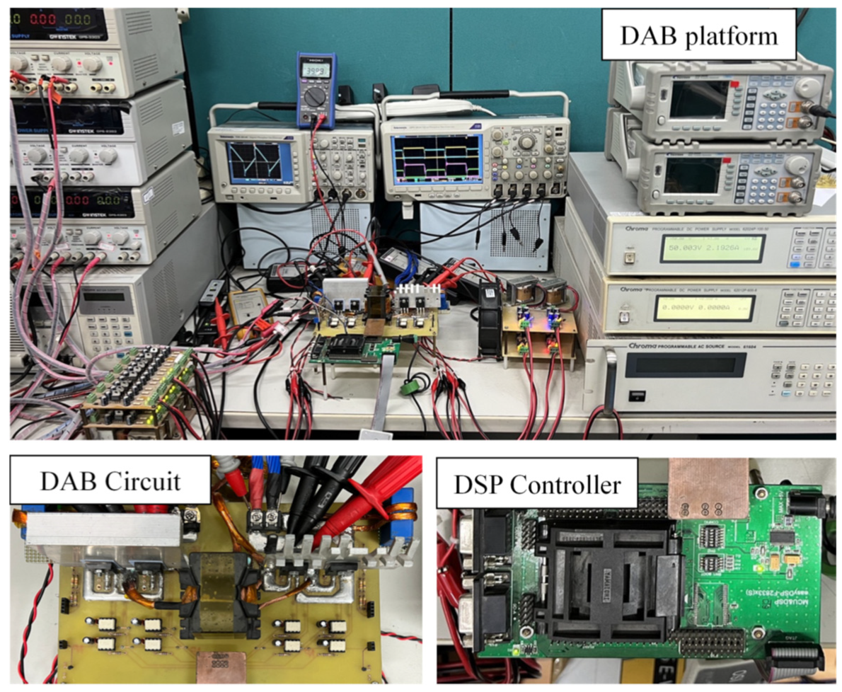
As a practical demonstration of the proposed dual-mode control strategy, a prototype DAB converter with a power rating of 1 kW was built and tested. The image of the actual circuit experimental platform is presented in Figure 11.
In this experiment, the prototype converter uses a DSP TMS320F28335 produced by Texas Instruments (Dallas, TX, USA) as a digital controller to implement the proposed dual-mode control strategy. The proposed dual-mode DAB converter prototype has the specifications shown in Table 3:
Experimental data describing the bidirectional power conversion of the proposed DAB converter are divided into two categories: the measured waveforms of the forward power conversion mode (power flow from the high-voltage side to the low-voltage side) and the measured waveforms of the backward power conversion mode (power flow from the low-voltage side to the high-voltage side).

5.1. Forward Power Conversion Mode

According to the load conditions, the proposed DAB converter operates in PWM mode at light load (output power below 200 W), as shown in Figure 12 and Figure 13. In PWM mode control, the gate signals VGS1 and VGS3 on the high-voltage side are synchronized with gate signals VGS5 and VGS7 on the low-voltage side. Thus, the DAB converter has the switching characteristics of a synchronous rectifier, as shown in Figure 12a and Figure 13a. In addition, it can be seen from Figure 12b that when the output power is 10 W, the duty cycle of gate signal VGS1 is approximately 45.7%, and the RMS value of inductor current iLK is 278 mA. When the output power increases to 200 W, the duty cycle of the gate signal VGS1 increases to 47.1%, and the RMS value of inductor current iLK is 739 mA, as shown in Figure 13b.
When the output power increases above 200 W, the operating mode of the proposed DAB converter changes from PWM mode to SPS mode, as shown in Figure 14 and Figure 15. The SPS controls the turn-on time of switches, causing the phase-shift between the high-voltage side switches and low-voltage side switches, thereby controlling the direction and magnitude of power flow. When VGS1 leads VGS5, power flows from the high-voltage side to the low-voltage side, as illustrated in Figure 14a and Figure 15a. When the output power is 300 W and 1 kW, the RMS value of inductor current iLK is 852 mA and 2.81 A, respectively, as shown in Figure 14b and Figure 15b.

5.2. Backward Power Conversion Mode

Since the main control object in this mode is changed to the low-voltage side, the main control signals are VGS5, VGS6, VGS7, and VGS8. At light load (output power below 100 W), the DAB converter operates in PWM mode, as shown in Figure 16 and Figure 17. In PWM mode control, gate signals VGS5 and VGS7 on the low-voltage side are in phase with gate signals VGS1 and VGS3 on the high-voltage side. Thus, the DAB converter has the switching characteristics of a synchronous rectifier, as shown in Figure 16a and Figure 17a. According to Figure 16b and Figure 17b, when the output power is 10 W and 100 W, the duty cycle of gate signal VGS7 is approximately 43.44% and 46.29%, and the inductor current iLK is 269 mA and 298 mA, respectively.
When the output power increases above 100 W, the operating mode of the proposed DAB converter changes from PWM mode to SPS mode. Note that at this time, gate signal VGS1 lags behind gate signal VGS5, as shown in Figure 18a and Figure 19a. When the output power is 200 W and 1 kW, the RMS value of inductor current iLK is 595 mA and 2.84 A, respectively, as shown in Figure 18b and Figure 19b.

5.3. Load Transient Testing for the Proposed DAB Converter

Experiments on the step load response of the proposed converter in bidirectional power conversion are shown in Figure 20 and Figure 21. Figure 20 shows the experimental waveforms in the forward power conversion mode. According to Figure 20a, the distortion level of battery voltage is approximately 12 V when the step load changes from 10 W to 1 kW, and it takes about 300 ms to reach a steady state. Conversely, the distortion level of battery voltage is approximately 2 V when the step load changes from 1 kW to 10 W, and it takes about 200 ms to reach a steady state, as shown in Figure 20b. Figure 21 shows the experimental waveforms in the backward power conversion mode. When the step load changes from 10 W to 1 kW, the distortion level of the DC bus voltage is approximately 5 V, and it takes around 10 ms to reach a steady state, as shown in Figure 21a. Conversely, when the step load changes from 1 kW to 10 W, the distortion level of the DC bus voltage is around 5 V, and it takes about 120 ms to reach a steady state, as shown in Figure 21b.
Figure 22 and Figure 23 are waveforms of the mode switching of the proposed DAB converter. This paper sets the mode switching point at 200 W for forward power conversion, so the output power is selected from 150 W to 300 W for measurement. According to Figure 22a, it takes approximately 60 µs for the converter to reach a steady state without oscillation when the output power increases from 150 W to 300 W. Conversely, when the output power changes from 300 W to 150 W, the converter takes approximately 100 µs to reach a steady state without oscillation, as shown in Figure 22b.
For backward power conversion, the mode switching point (threshold value) is set at 100 W, so the output power is selected from 10 W to 200 W for measurement. A steady state time of about 60 µs is observed when the output power increases from 10 W to 200 W in Figure 23a. Conversely, when the output power decreases from 200 W to 10 W, the converter reaches a steady state after 120 µs, as shown in Figure 23b. It is worth noting that under the above test conditions, the converter does not oscillate. Therefore, the dual-mode control strategy proposed in this paper is feasible.

5.4. Efficiency Comparison Curve

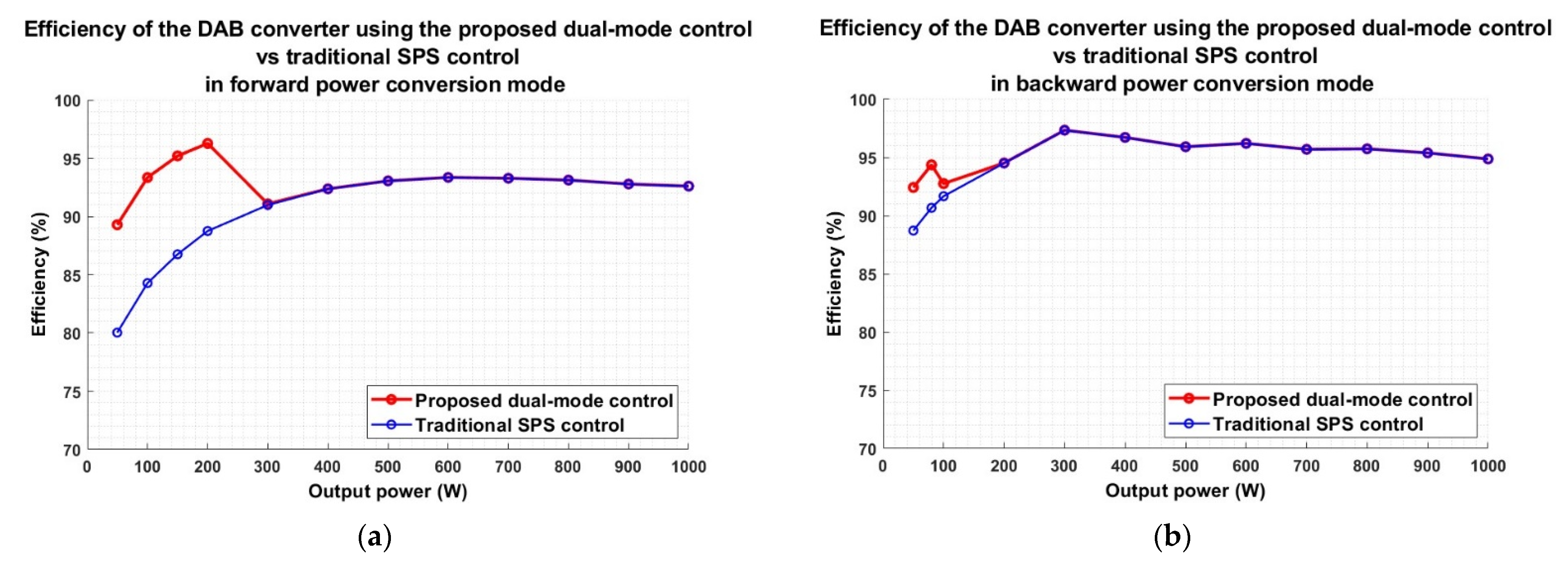
Figure 24 shows the efficiency comparison between the DAB converter using the dual-mode control strategy proposed in this paper and a DAB converter using the traditional SPS control strategy. It can be seen from the figure that the light load efficiency of the DAB converter using the dual-mode control strategy is better than that of the DAB converter using the traditional SPS strategy. In particular, in the forward power conversion mode, the maximum efficiency of the proposed control strategy is 10% higher than that of the traditional SPS strategy, as shown in Figure 24a. In the backward power conversion mode, the maximum efficiency of the proposed control strategy is 5% higher than that of the traditional SPS control strategy, as shown in Figure 24b.
The characteristic of the SPS control is that high backflow power when operating at light loads reduces the converter efficiency. The light-load efficiency of the proposed dual-mode converter is enhanced because the converter operates in PWM mode to minimize backflow power. Experimental results verify that the dual-mode control strategy proposed in this paper improves the light load efficiency of the DAB converter compared with the traditional SPS control strategy. Table 4 shows a comparison of the related studies with the proposed dual-mode control strategy in terms of efficiency. Table 5 also shows the calculation for the power loss of the proposed dual-mode DAB converter at a load of 100 W.

6. Conclusions

This paper proposes a dual-mode control strategy for addressing the disadvantage of conventional SPS control applied to DAB converters. In dual-mode control, PWM and SPS techniques are combined and switched depending on the load. Under light load conditions, the DAB converter is controlled by the PWM control method. During medium-to-full load conditions, on the other hand, the DAB converter is controlled by the SPS method. The experimental results indicate that the converter can achieve the highest efficiency of 96.267% when operating in the forward power conversion mode (power flow from the high-voltage side to the low-voltage side), and 97.331% when operating in the backward power conversion mode (power flow from the low-voltage side to the high-voltage side). Furthermore, there is no oscillation when switching back and forth between operating modes.

Author Contributions

Conceptualization, J.-M.W. and T.N.T.T.; methodology, W.-Y.C. and J.-M.W.; software, T.N.T.T., W.-Y.C. and J.-M.W.; validation, T.N.T.T., W.-Y.C. and J.-M.W.; resources, J.-M.W.; writing—original draft preparation, J.-M.W. and T.N.T.T.; writing—review and editing, J.-M.W. and T.N.T.T. All authors have read and agreed to the published version of the manuscript.

Funding

This research was funded by the Ministry of Science and Technology, R.O.C., (grant numbers: MOST 110-2622-E-150-002 and MOST 111-2221-E-150-009).

Institutional Review Board Statement

Not applicable.

Informed Consent Statement

Not applicable.

Data Availability Statement

Not applicable.

Acknowledgments

The authors are grateful for the support of Power Electronics Research Laboratory members during the execution of this study. Further, we would like to express sincere gratitude to all anonymous reviewers for their time and expertise, which significantly improved our paper’s academic and professional quality.

Conflicts of Interest

The authors declare no conflict of interest.

References

  1. European Commission; Directorate-General for Research and Innovation; European SmartGrids Technology Platform. European SmartGrids Technology Platform: Vision and strategy for Europe’s Electricity Networks of the Future; European Commission: Brussels, Belgium, 2006. [Google Scholar]
  2. Can, E. A new multi-level inverter with reverse connected dual dc to dc converter at simulation. Int. J. Model. Simul. 2022, 42, 34–46. [Google Scholar] [CrossRef]
  3. Costinett, D.; Maksimovic, D.; Zane, R. Design and control for high efficiency in high step-down dual active bridge converters operating at high switching frequency. IEEE Trans. Power Electron. 2012, 28, 3931–3940. [Google Scholar] [CrossRef]
  4. De Doncker, R.W.; Divan, D.M.; Kheraluwala, M.H. A three-phase soft-switched high-power-density DC/DC converter for high-power applications. IEEE Trans. Ind. Appl. 1991, 27, 63–73. [Google Scholar] [CrossRef]
  5. Inoue, S.; Akagi, H. A bidirectional isolated DC–DC converter as a core circuit of the next-generation medium-voltage power conversion system. IEEE Trans. Power 2007, 22, 535–542. [Google Scholar] [CrossRef]
  6. Steigerwald, R.L.; De Doncker, R.W.; Kheraluwala, H. A comparison of high-power DC-DC soft-switched converter topologies. IEEE Trans. Ind. Appl. 1996, 32, 1139–1145. [Google Scholar] [CrossRef]
  7. Lenke, R.; Mura, F.; De Doncker, R.W. Comparison of non-resonant and super-resonant dual-active ZVS-operated high-power DC-DC converters. In Proceedings of the 2009 13th European Conference on Power Electronics and Applications, Barcelona, Spain, 8–10 September 2009; pp. 1–10. [Google Scholar]
  8. Ren, Y.; Xu, M.; Sun, J.; Lee, F.C. A family of high power density unregulated bus converters. IEEE Trans. Power Electron. 2005, 20, 1045–1054. [Google Scholar] [CrossRef]
  9. Krismer, F.; Kolar, J.W. Accurate power loss model derivation of a high-current dual active bridge converter for an automotive application. IEEE Trans. Ind. Electron. 2009, 57, 881–891. [Google Scholar] [CrossRef]
  10. Shi, H.; Wen, H.; Chen, J.; Hu, Y.; Jiang, L.; Chen, G.; Ma, J. Minimum-backflow-power scheme of DAB-based solid-state transformer with extended-phase-shift control. IEEE Trans. Ind. Appl. 2018, 54, 3483–3496. [Google Scholar] [CrossRef]
  11. Chakraborty, S.; Chattopadhyay, S. Fully ZVS, minimum RMS current operation of the dual-active half-bridge converter using closed-loop three-degree-of-freedom control. IEEE Trans. Power Electron. 2018, 33, 10188–10199. [Google Scholar] [CrossRef]
  12. Yan, Y.-H.; Cheng, H.-L.; Chan, S.-Y.; Chen, Y.-D.; Chang, Y.-N. Design of an Isolated Bidirectional Symmetric Resonant Converter. Appl. Sci. 2020, 10, 8144. [Google Scholar] [CrossRef]
  13. Wu, J.; Li, Y.; Sun, X.; Liu, F. A new dual-bridge series resonant DC–DC converter with dual tank. IEEE Trans. Power Electron. 2017, 33, 3884–3897. [Google Scholar] [CrossRef]
  14. TDK. Mn-Zn Ferrite Cores for Switching Power Supplies PQ Series. Available online: https://product.tdk.com/system/files/dam/doc/product/ferrite/ferrite/ferrite-core/catalog/ferrite_mz_sw_pq_en.pdf (accessed on 28 September 2022).
  15. Pressman, A. Switching Power Supply Design; McGraw-Hill Education: New York, NY, USA, 2009. [Google Scholar]
  16. Design Guide: TIDA-010054 Bidirectional, Dual Active Bridge Reference Design for Level 3 Electric Vehicle Charging Stations. 2019. Available online: https://www.ti.com/document-viewer/lit/html/TIDUES0C/GUID-714D036F-89AA-4176-B535-67496BDA93E6#TITLE-TIDUES0ID-7516C1F1-8B53-4F6E-D989-7869B3181718 (accessed on 29 September 2022).
  17. Gladish, J.; Semiconductor, F. MOSFET Selection to Minimize Losses in Low-Output-Voltage DC-DC Converters Fairchild Semiconductor Power Seminar 2008–2009. Available online: https://nanopdf.com/download/mosfet-selection-to-minimize-losses-in-low-output_pdf (accessed on 29 September 2022).
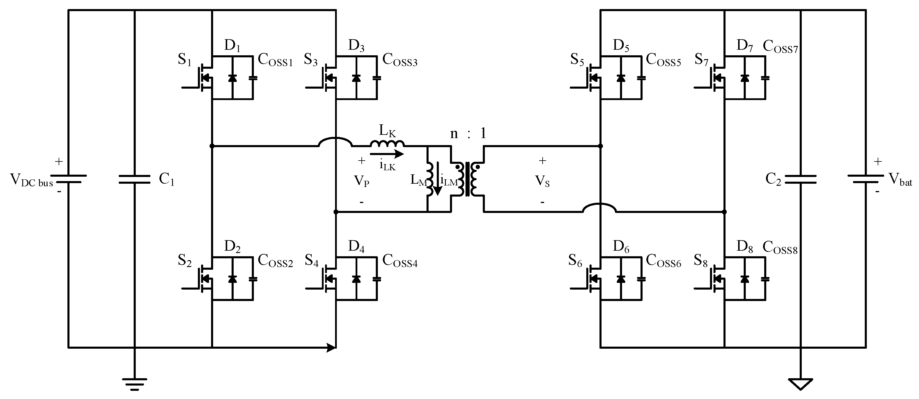
Figure 1. The DAB converter topology.
Applsci 12 12356 g001
Figure 2. Control waveforms of SPS control.
Applsci 12 12356 g002
Figure 3. Backflow power in SPS control.
Applsci 12 12356 g003
Figure 4. Circuit structure of the DAB converter.
Applsci 12 12356 g004
Figure 5. Theoretical waveforms of the proposed control strategy for the DAB converter in PWM mode under light load conditions.
Applsci 12 12356 g005
Figure 6. (af) The current flow path of the DAB converter in PWM control mode.
Applsci 12 12356 g006
Figure 7. Theoretical waveforms of the proposed control strategy for the DAB converter in SPS mode under medium-to-full load conditions.
Applsci 12 12356 g007
Figure 8. (ag) The current flow path of the DAB converter in SPS control mode.
Applsci 12 12356 g008
Figure 9. Block diagram of the proposed dual-mode control for the DAB converter.
Applsci 12 12356 g009
Figure 10. Design flow chart for energy storage components.
Applsci 12 12356 g010
Figure 11. Experimental platform of DAB in laboratory.
Applsci 12 12356 g011
Figure 12. Experimental waveforms of the prototype converter operating in forward power conversion mode (at 10 W output power): (a) waveforms of gate signals VGS1, VGS3, VGS5 and VGS7; (b) waveforms of gate signals VGS1, VGS3, and inductor current iLK.
Applsci 12 12356 g012
Figure 13. Experimental waveforms of the prototype converter operating in forward power conversion mode (at 200 W output power): (a) waveforms of gate signals VGS1, VGS3, VGS5 and VGS7; (b) waveforms of gate signals VGS1, VGS3, and inductor current iLK.
Applsci 12 12356 g013
Figure 14. Experimental waveforms of the prototype converter operating in forward power conversion mode (at 300 W output power): (a) waveforms of gate signals VGS1, VGS3, VGS5 and VGS7; (b) waveforms of gate signals VGS1, VGS3 and inductor current iLK.
Applsci 12 12356 g014
Figure 15. Experimental waveforms of the prototype converter operating in forward power conversion mode (at 1 kW output power): (a) waveforms of gate signals VGS1, VGS3, VGS5 and VGS7; (b) waveforms of gate signals VGS1, VGS3 and inductor current iLK.
Applsci 12 12356 g015
Figure 16. Experimental waveforms of the prototype converter operating in backward power conversion mode (at 10 W output power): (a) waveforms of gate signals VGS1, VGS3, VGS5 and VGS7; (b) waveforms of gate signals VGS5, VGS7 and inductor current iLK.
Applsci 12 12356 g016
Figure 17. Experimental waveforms of the prototype converter operating in backward power conversion mode (at 100 W output power): (a) waveforms of gate signals VGS1, VGS3, VGS5 and VGS7; (b) waveforms of gate signals VGS5, VGS7 and inductor current iLK.
Applsci 12 12356 g017
Figure 18. Experimental waveforms of the prototype converter operating in backward power conversion mode (at 200 W output power): (a) waveforms of gate signals VGS1, VGS3, VGS5 and VGS7; (b) waveforms of gate signals VGS5, VGS7 and inductor current iLK.
Applsci 12 12356 g018
Figure 19. Experimental waveforms of the prototype converter operating in backward power conversion mode (at 1 kW output power): (a) waveforms of gate signals VGS1, VGS3, VGS5 and VGS7; (b) waveforms of gate signals VGS5, VGS7 and inductor current iLK.
Applsci 12 12356 g019
Figure 20. Step load response of prototype converter operating in forward power conversion mode: (a) load change from 10 W to 1 kW; (b) load change from 1 kW to 10 W.
Applsci 12 12356 g020
Figure 21. Step load response of prototype converter operating in backward power conversion mode: (a) load change from 10 W to 1 kW; (b) load change from 1 kW to 10 W.
Applsci 12 12356 g021
Figure 22. Waveforms of mode switching (in forward power conversion): (a) load change from 150 W to 300 W; (b) load change from 300 W to 150 W.
Applsci 12 12356 g022
Figure 23. Waveforms of mode switching (in backward power conversion): (a) load change from 10 W to 200 W; (b) load change from 200 W to 10 W.
Applsci 12 12356 g023
Figure 24. Comparison of the efficiency of the DAB converter using the proposed dual-mode control strategy and a DAB converter using the traditional SPS control strategy: (a) forward power conversion mode; (b) backward power conversion mode.
Applsci 12 12356 g024
Table 1. Comparison of the DAB converter with different control strategies.
ItemProposedRef. [10]Ref. [12]
TopologyDABDABSRDAB
Control strategyDual-mode PWM-SPSMEPSPFM
Transformer typeConventional transformerSolid-state transformerConventional transformer
Prototype power rating1 kW200 W1 kW
Switching frequency100 kHz20 kHz70–150 kHz
Maximum efficiency97.30%pprox. 90.00%94.60%
Table 2. Design parameters of the DAB converter prototype.
ParametersValue
Primary voltage, VDcbus400 V
Secondary voltage, Vbat50 V
Maximum output power, Po,max1 kW
Maximum power, PMax4.5 kW
Switching frequency, fsw100 kHz
Maximum phase-shift, Dmax0.2
Voltage ripple, ΔVDcbus, ΔVbat<5%
Table 3. Specifications of the proposed DAB converter prototype.
ParametersValue
Primary voltage, VDcbus400 V
Secondary voltage, Vbat50 V
Transformer turns ratio, n24:3
Maximum output power, Po,max1 kW
Switching frequency, fsw100 kHz
Maximum phase-shift, Dmax0.2
Magnetizing inductance, LM1.2 mH
Leakage inductance, LK57 µH
High-voltage side capacitor, C1100 µF
Low-voltage side capacitor, C2360 µF
Table 4. Efficiency comparison of the DAB converter with different control strategies in forward power conversion.
Load ConditionProposedRef. [10]Ref. [12]
Light load (10% of power rating)93.34%n/aapprox. 86%
Medium load (50% of power rating)93.04%approx. 88%approx. 92%
Full load (100% of power rating)92.59%approx. 90%93.25%
Table 5. Power loss calculations for the prototype converter at 100 W.
ItemModel No.ParameterPower Loss
Pri. (S1~S4)SCT3080ALGC11RDS(ON) = 80 mΩ; Ciss = 571 pF; Crss = 19 pF1.769 W
Sec. (S5~S8)IRFP4321PBFRDS(ON) = 12 mΩ; Ciss = 4460 pF; Crss = 82 pF2.385 W
TransformerPC95PQ50/50Z-12PCV(Tr) = 39,810 W/m3; Ve(Tr) = 37.2 × 10⁻⁶ m3; RCopper(Pri) = 3.35 Ω; RCopper(Sec) = 0.0155 Ω1.499 W
InductorCM467125PCV(In) = 40 × 103 W/m3; Ve(In) = 21.373 × 10⁻⁶ m3; RCopper(In) = 0.2554 Ω0.813 W
Publisher’s Note: MDPI stays neutral with regard to jurisdictional claims in published maps and institutional affiliations.