Abstract
Deep electrochemical etching (DEE) is proposed in this paper. DEE is a process that repeats steps consisting of electrodeposition, laser patterning, and electrochemical etching. In the electrodeposition step, a deposited layer is formed on the surface of the workpiece. This deposited layer serves as a protective layer to protect the surface of the workpiece until it is completely dissolved in the electrochemical etching step. Laser patterning is the step of patterning a deposited layer by irradiating a laser beam while minimizing surface damage to the workpiece. The etching of the workpiece proceeds through the electrochemical etching step. If these three steps are performed sequentially, one cycle of the DEE process is completed. By repeating this cycle, an improved etch factor can be obtained in the DEE process. The processing characteristics according to DEE process conditions were analyzed through an SEM and 3D surface profiler. Through the DEE process, a microstructure with a deep etching depth was fabricated, and the micropatterns successfully penetrated a one-hundred-um-thick stainless steel specimen. Through the DEE process, it was confirmed that it is possible to fabricate a micro with a high aspect ratio structure pattern by improving the etch factor.
1. Introduction
Recently, attempts to fabricate microstructures with high aspect ratio patterns in metal are increasing. Microstructures with a high aspect ratio using metal are used in satellite cryogenic coolers, ABS brake systems, gasoline direct fuel injection, motor laminations, automotive interior trim, heat exchanger plates, medical devices, dental membranes, electrical connectors and contacts, bipolar plates, microstrip antennas, microchannel fabrication, and high-aspect-ratio cooling holes. As a technology for realizing the fabrication of such a microstructure pattern with a high aspect ratio, microelectrochemical machining (ECM) can be an alternative. Micro-ECM can be applied to diverse alloys, which are conductive materials and have been used in various fields, such as machinery, aviation, electronics, and the defense industry [1,2,3]. The micro-ECM of metals is largely divided into two types. One is electrochemical machining using ultrashort voltage pulses and the other is electrochemical etching using a photomask.
ECM using ultrashort pulses is a processing method that can realize high precision. However, the disadvantages are that it takes a lot of time, and there is a high cost to manufacture a microtool. In ECM using ultrashort voltage pulses, there is a limit to increasing the machining speed because the average current density of ultrashort pulses is not high. Various studies have been conducted to overcome these problems. Micro-ECM using a multitool has been attempted, but the limitation of the machining speed has not been overcome [4]. There have been studies that tried to process holes with a high aspect ratio using laser-assisted electrochemical machining, but it is not suitable for application to complex machining shapes or large areas [5,6,7].
Electrochemical etching using a photomask is suitable for processing a large area because it uses a DC power supply or long pulse voltages. However, manufacturing a photomask requires complicated procedures and expensive equipment. In addition, the electrochemical etching process using a photomask has limitations in the shape that can be processed due to the limitation of the etch factor, so the application fields are limited to surface polishing, surface texturing, surface patterning, and thin-plate penetration shape fabrication. Research to improve the etch factor in electrochemical etching has also been reported. Although research on backside wet etching using laser beams has been conducted, there is a limit in that the scope of application is limited to the processing of glass materials [8]. In electrochemical etching using laser masking, it was possible to process a large area without a photomask, but it did not escape the limitations of the etch factor [9,10]. Studies on the reduction of undercutting using oxygen generation in the anode electrode have been reported, but there is a limit to the improvement of the aspect ratio [11]. Research has been made on the process of simultaneously etching both surfaces by fabricating a photomask on both sides of a metal, but there is a limit to increasing the etch factor greater than 3 [1].
In order to broaden the application range of microelectrochemical processing of metals in various fields, it can be applied to a large area, and the etch factor should be improved. In this aspect, in order to increase the average current density compared to micro-ECM using ultrashort pulses with a low average current density, electrochemical etching using DC voltage or long pulse voltages is advantageous for large-area processing. In addition, if electrochemical etching can prevent side etching, a shape with an improved etch factor can be obtained over a large area. Among the etching methods, there is already dry etching technology, such as deep reactive ion etching (DRIE), which is capable of fabricating microstructures with a high aspect ratio by blocking side etch [12]. However, dry etching such as DRIE is only applicable to a limited number of metals or materials, such as silicon. Therefore, in order to be applicable to various metals, side etching must be prevented or minimized even in electrochemical etching.
Minimizing side etch in electrochemical etching means that it is possible to fabricate microstructures with a high aspect ratio and deep etching in various metals. Recently, a study on the electrochemical etching of metal using laser patterning of a deposited copper layer has been reported [13]. Electrochemical etching of metal using laser patterning is a study that provided a clue showing side etch can be minimized using the deposited copper layer as a protective layer.
In this study, a new processing technology was proposed to improve the etch factor limit in electrochemical etching and to fabricate a microstructure with a high aspect ratio even in wet etching. In this paper, this new process is named the DEE process. The DEE process consists of sequentially performing electrodeposition, laser patterning, and electrochemical etching in one cycle. This cycle was repeated to allow deep etching of the metal. Changes in the etching characteristics of the DEE process according to the number of cycles were investigated. The experimental results of the DEE process were analyzed through an SEM and 3D surface profiler. Finally, a side wall with a deep depth and penetrating microstructures was successfully fabricated.
2. Experimental System
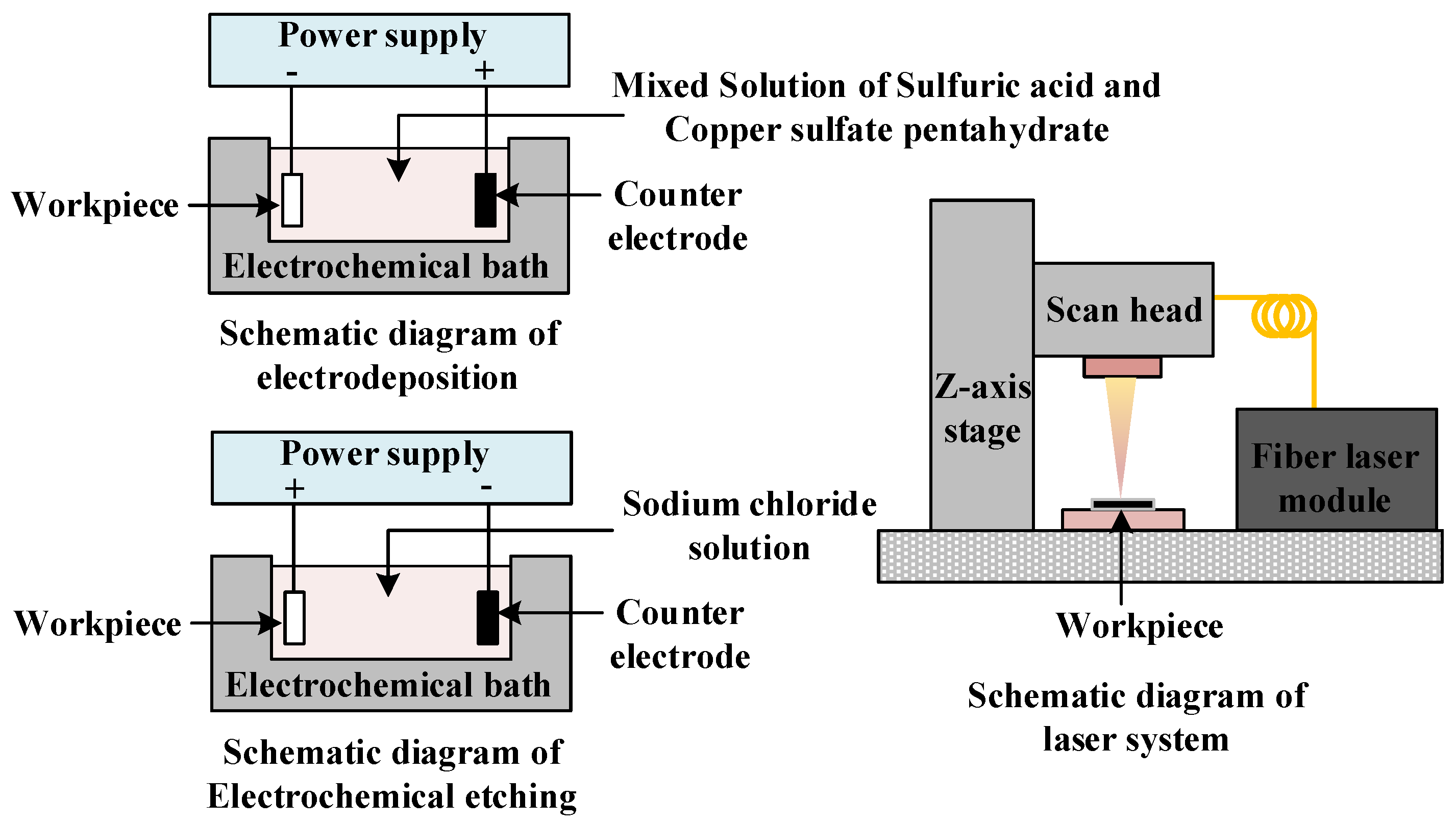
Figure 1 is the schematic diagram of the experimental setup for DEE process. In the DEE process, an electrochemical cell and a JIG for electrodes for electrodeposition and electrochemical etching processes were used. A copper plate with a width of 1 mm, length of 2 mm, and thickness of 3 mm was used as a counter electrode. A stainless steel plate with a width of 1 mm and a length of 2 mm was used as a workpiece electrode. During electrodeposition, a copper layer was deposited on the surface of AISI304 stainless steel using an aqueous solution of 0.5 M sulfuric acid and 0.5 M copper sulfate pentahydrate. In electrochemical etching, deposited stainless steel was used as a workpiece, and a copper plate was used as a counter electrode. 2 M sodium chloride aqueous solution was used as etchant in electrochemical etching. DC power supply was used to supply current during electrodeposition and electrochemical etching processes.
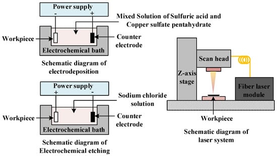
Figure 1.
Experimental setup for deep electrochemical etching (DEE).
The deposited layer was patterned using a ytterbium pulsed fiber laser system (IPG photonics, YLPM series). The laser beam was transferred using a galvanometer system (CAMBRIDGE technology, PS1-10®). Table 1 shows the specifications of the ytterbium pulsed fiber laser module and galvanometer scanning module. After DEE process, surface profiles were measured by confocal laser scanning microscope (NANOSCOPE SYSTEMS, NS-3500®).

Table 1.
Optical characteristics of ytterbium pulsed fiber laser beam.
3. Principle of DEE Process
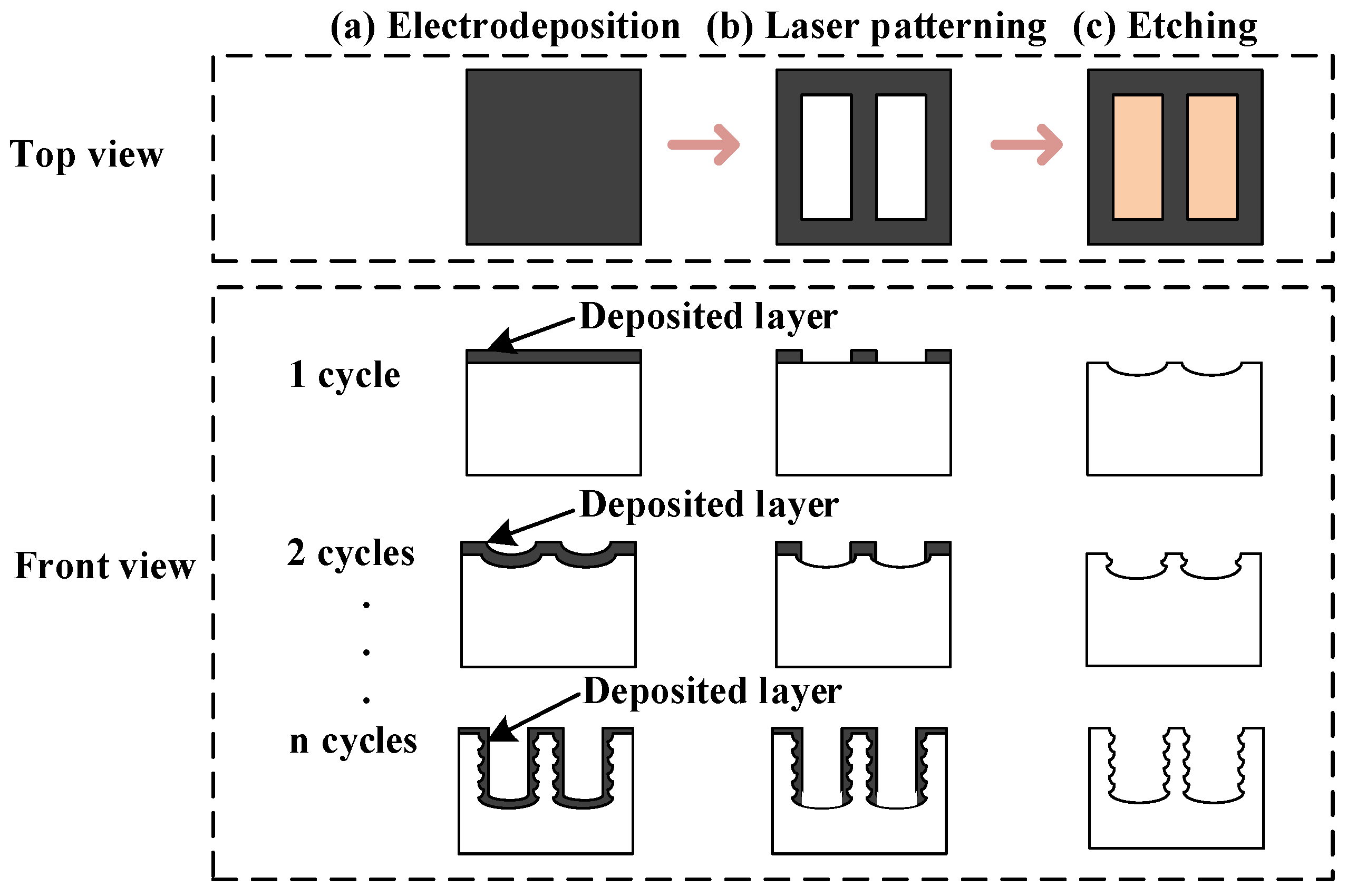
DEE is a process that repeats the electrodeposition, deposited layer patterning, and electrochemical etching steps in one cycle. Figure 2 is a diagram showing the DEE process. In the first step, electrodeposition, a deposited layer is created on the surface of a metal workpiece, as shown in Figure 2a. In this case, the deposited layer must be formed to have a uniform thickness while serving as a protective layer to enable uniform patterning of the deposited layer in the laser patterning step. In the second step, the deposited layer is patterned in the desired patterns using a laser beam, as shown in Figure 2b. At this time, the damage to the base metal surface by laser irradiation should be minimized. The third step is the electrochemical etching step in which the deposited layer and metal base material are simultaneously dissolved by the anodic dissolution, as shown in Figure 2c. During the electrochemical etching step, the anodic dissolution does not occur on the surface of the base material in the area covered by the deposited layer, and the anodic dissolution of the base material occurs only in the area where there is no deposited layer. The electrochemical etching step can be performed until the deposited layer is entirely dissolved. When the electrochemical etching step is finished, the difference in dissolved depth between the protected area of the workpiece by the deposited layer and the unprotected area of the workpiece is within a few micrometers. When these three steps are performed, one cycle of the DEE process is completed.

Figure 2.
Procedures for DEE process; (a) electrodeposition, (b) patterning by laser irradiation, and (c) electrochemical etching.
After the first cycle of the DEE process is completed, the cross-sectional shape of the metal specimen has a hemispherical profile. This is because isotropic etching proceeds in most metals. Therefore, if the electrodeposition step is performed in the second cycle of the DEE process, the deposited layer is formed along the hemispherical profile. In the laser patterning step, since the bottom surface of the deposited layer formed along the hemispherical shape is removed and the side deposited layer is left, the etching in the depth direction can be performed while minimizing the side etching in the electrochemical etching step.
Even in the second cycle, if the deposited layer is removed, the electrochemical etching must be stopped because side etch can no longer be prevented. Therefore, if the cycle consisting of electrodeposition, deposited layer patterning, and electrochemical etching is repeatedly performed, deep etching can be performed while minimizing side etch. Similar to the DRIE process, the DEE process can adjust the processing precision of vertical walls by adjusting the etching depth per cycle. In addition, the DEE process can also implement through-shaped patterns with a high aspect ratio.
4. Results and Discussion
4.1. Shape Evolution of DEE Process Conditions
A copper layer was deposited on the stainless steel surface through an electrodeposition process. A copper-deposited layer was formed under the conditions of 0.5 M of sulfuric acid, 0.5 M of copper sulfate mixed solution, an applied voltage of 2 V, and an electrodeposition time of 60 s. Shin et al. [13] suggested laser beam irradiation conditions to minimize damage to the surface of stainless steel, the base material. In this study, the copper layer was removed under conditions that minimized the surface damage of stainless steel, which is the base material [13]. The laser patterning conditions of the deposited layer in the DEE process are shown in Table 2. In order to minimize damage to the base material, the copper layer was removed by performing laser patterning three times under the laser beam conditions in Table 2. Figure 3 shows the result of the actual patterning of the copper layer under the conditions of Table 2 as an optical image. The dark areas are the copper layer, and the light areas are the surface of the stainless steel from which the copper layer has been removed.
Table 2.
Laser patterning conditions of copper layer.

Figure 3.
Optical image of laser-patterned copper layer.
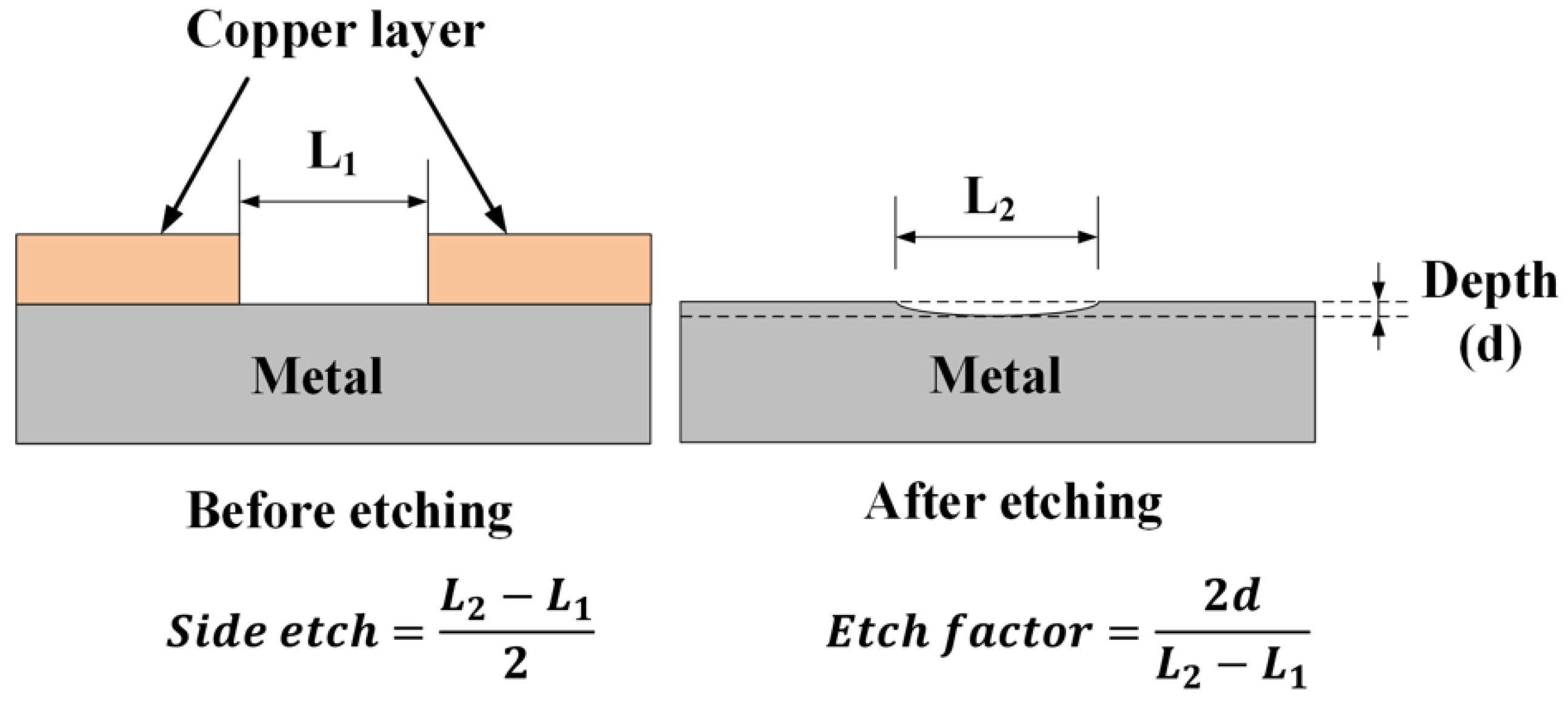
The electrochemical etching of metals is basically isotropic etching. Therefore, in the DEE process, the etching shape changes depending on the etching step conditions. Figure 4 shows the shape change of the cross-section in isotropic etching. As shown in Figure 4, in electrochemical etching, the etch factor is determined by the side etch and etching depth. Since the electrochemical etching of the DEE process is based on the isotropic etching of the metal, in order to increase the overall etching depth in the DEE process, side etching should be minimized. In the electrochemical etching of metal, the limit of the physical etch factor is about 1.5 [1,2,3]. If the etching time is excessive in the electrochemical etching step of the DEE process, it means that the etching proceeded even after the deposited layer protecting the sidewall was removed. If the side wall is not protected, the surface profile of the cross-section proceeds in a hemispherical shape, so the taper angle of the vertical wall in the etched final shape increases. The big taper angle of the vertical wall per cycle of the DEE process means that the precision of the overall machining shape is lowered after the DEE process is finished. Therefore, it is necessary to select an electrochemical etching depth per cycle of the DEE process that can minimize the taper angle. In the DEE process, the etch factor can be calculated by measuring the width before electrochemical etching as L1, the width at the repeated cycles as L2, and the total depth in the cycle as d.
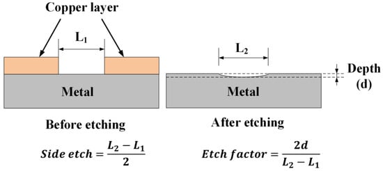
Figure 4.
Shape evolution and etch factor in electrochemical etching.
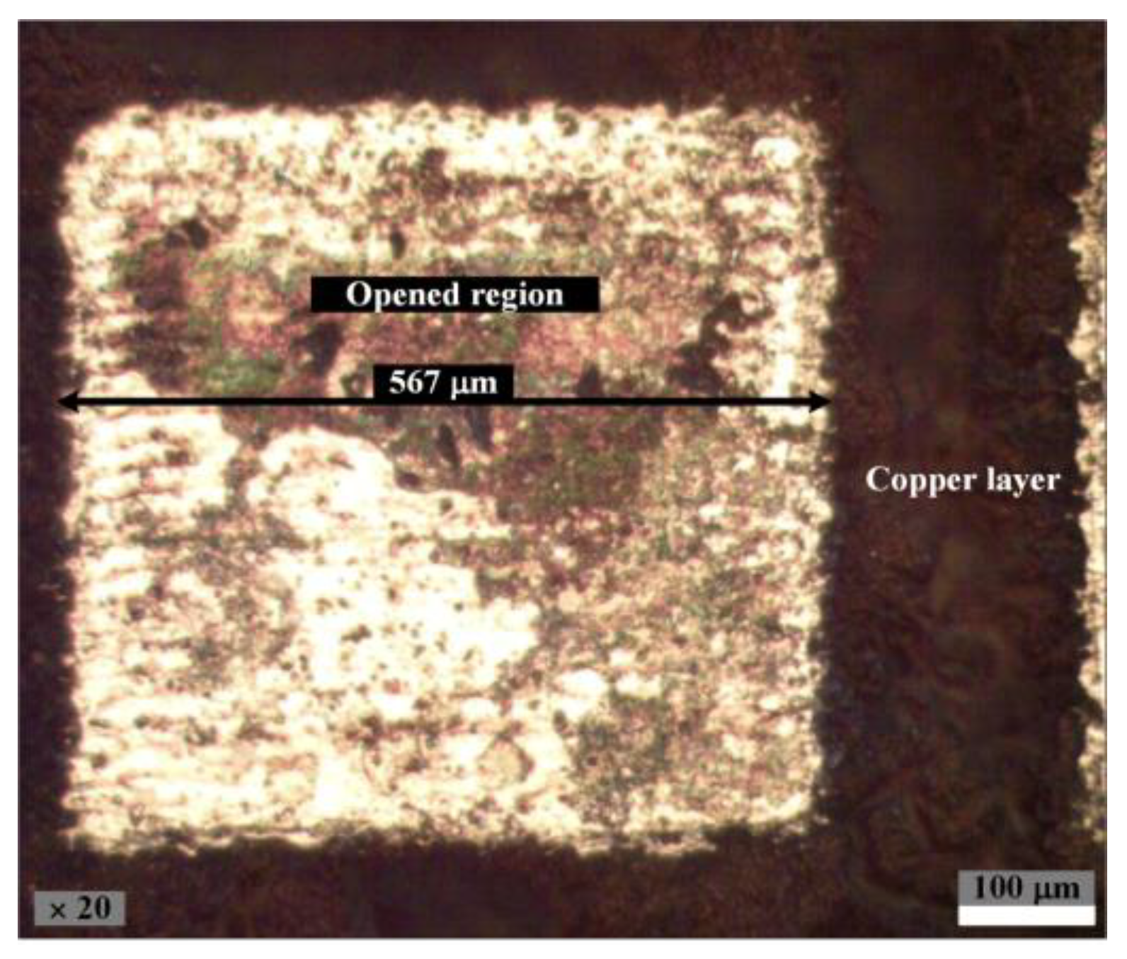
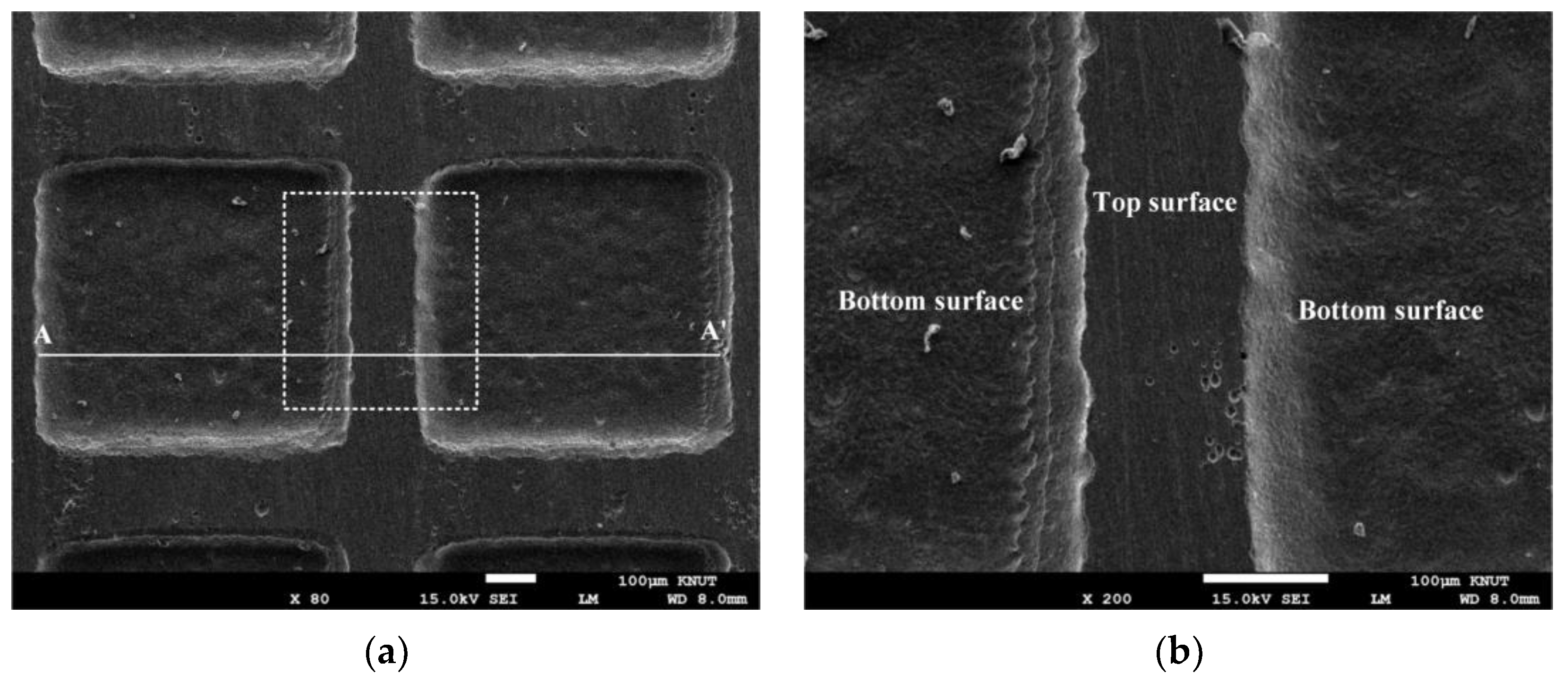
Figure 5 shows the result of a square pattern performed by repeating the DEE process 10 times at an excessive etching time of 10 s. Figure 5b is an enlarged picture of the white square dotted line in Figure 5a. As shown in Figure 5b, it can be seen that the taper angle is large in the vertical wall formed from the top surface to the bottom surface. This means that the more the DEE process was repeated under excessive etching conditions, the greater the taper angle was generated. In Figure 6, it can be confirmed that a big taper angle occurred as a result of measuring the surface profile of the cross-section of line AA’ in Figure 5a. This is because the side etches proceeded even after the copper layer was removed due to an excessive etching time in the etching step. If the DEE process is repeated under the condition of having an excessive etching time, a very big taper angle is generated, and the shape of the vertical wall becomes irregular. Therefore, in order to minimize irregular shape of the side wall in the DEE process, an appropriate etching time condition per cycle of the DEE process is required. Shin et al. confirmed that an excessive taper angle occurs when the etching time exceeds 10 s in selective electrochemical etching using a copper layer formed at 2 V with a 60 s condition [13]. In the DEE process, in order to minimize the taper in one cycle, an etching time of fewer than 10 s should be selected.

Figure 5.
SEM image of taper angle after repeating DEE process 10 times at excessive etching time (etching voltage: 10 V, etching time: 10 s): (a) square pattern; (b) magnified image of the square dotted line area in (a).
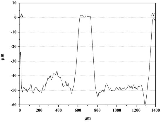
Figure 6.
Surface profile of the cross-section of line AA’ in Figure 5a.
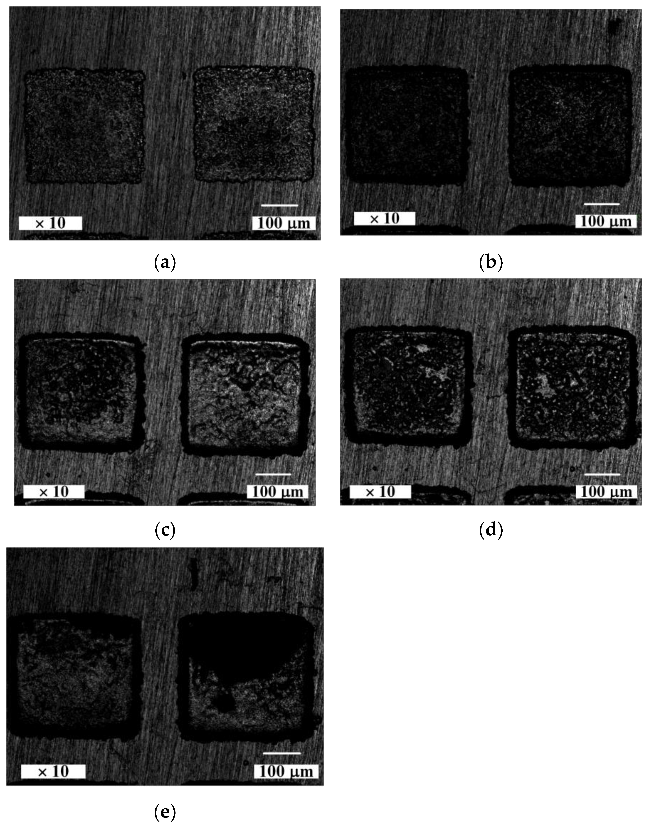
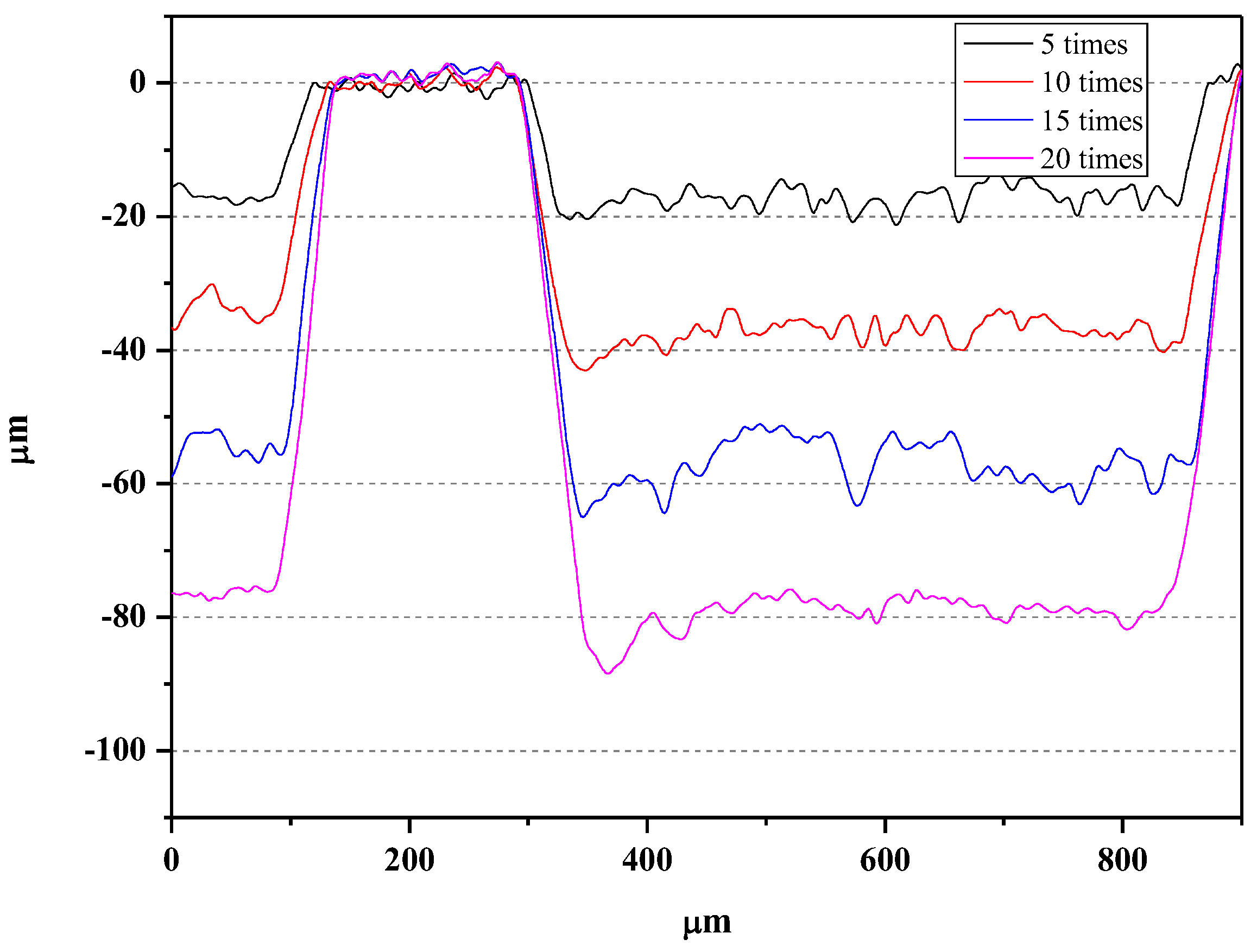
Figure 7a is a picture of one cycle of the DEE process completed by performing electrochemical etching after laser patterning of the deposited layer. Figure 7b–e is the results of performing the DEE process five times, 10 times, 15 times, and 20 times, respectively. Electrodeposition conditions are 2 V and 60 s, and laser patterning conditions are shown in Table 2. Figure 7c is an optical image when the number of repeated cycles in the DEE process is 10 times, and the etching depth at this time is about 37 μm. Figure 7e is an optical image when the number of repeated cycles in the DEE process is 20 times, and the etching depth at this time is about 81.6 μm. As shown in Figure 8, as the number of repeated cycles increases in the DEE process, the etching depth increases. As shown in Figure 8, as the number of repeated cycles increases up to five, it can be seen that the average depth of 20 μm per cycle has been processed. This is for the experiment repeated 20 times and can be said to show reproducibility with an average etching depth of 4.08 μm per cycle.

Figure 7.
Shape change according to the number of repeated cycles of the DEE process cycle (etching voltage: 10 V, etching time: 7 s): (a) once; (b) five times; (c) 10 times; (d) 15 times; and (e) 20 times.
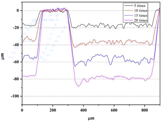
Figure 8.
The surface profile according to the number of repeated cycles in the DEE (etching voltage: 10 V, etching time: 7 s).
4.2. Deep Etching by the DEE process
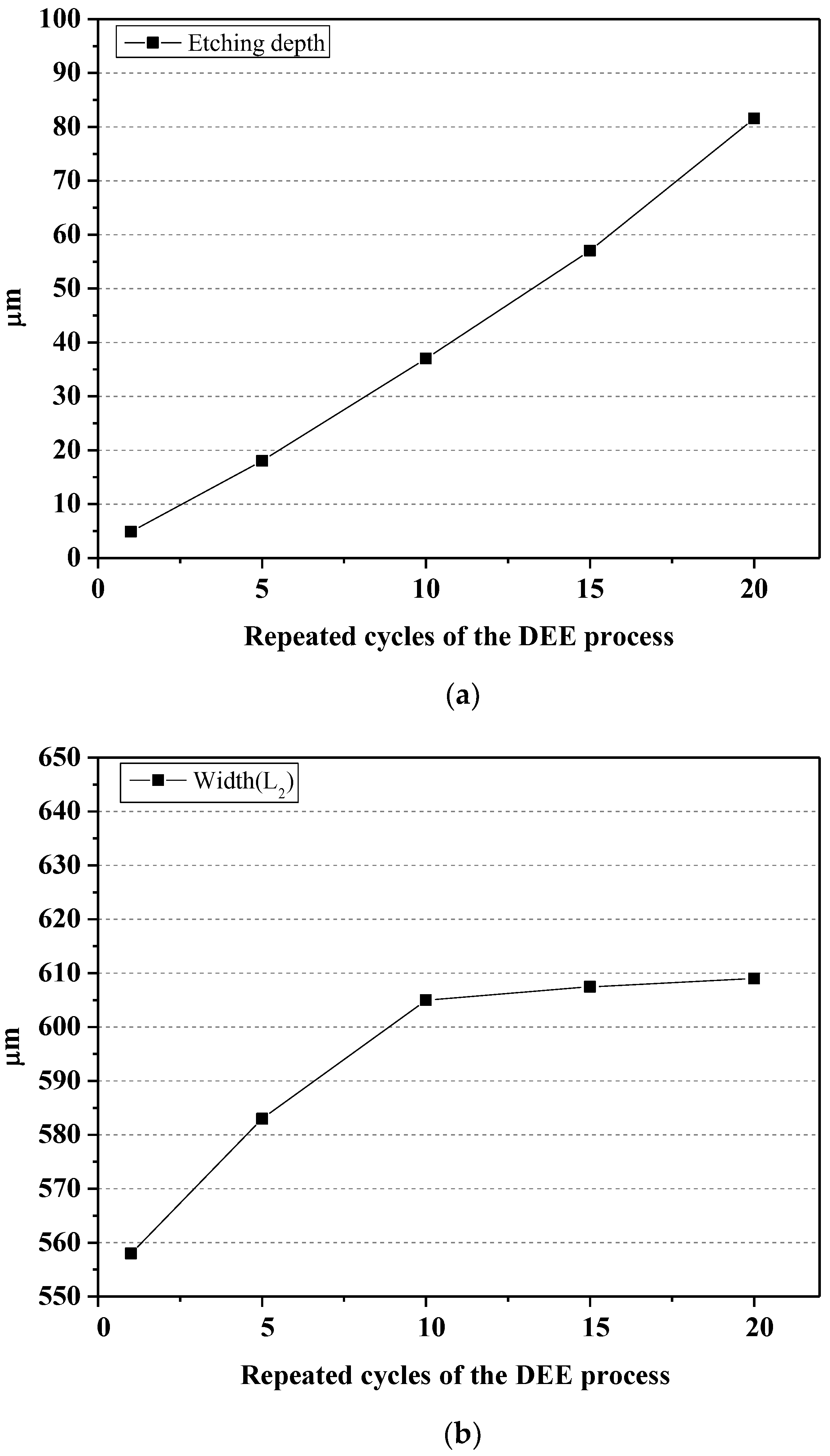
Figure 9a is a graph showing etching depth according to repeated cycles of the DEE process. As the number of repeated cycles in the DEE process increases, it can be seen that the etching depth increases almost linearly. The etching depth per cycle in the DEE process is about 4 μm. Figure 9b is a graph showing the width L2 according to repeated cycles of the DEE process. The width L2 increases significantly until the number of repeated cycles in the DEE process cycle is five, but the increase in width L2 is slightly slowed in the section from five to 10 repeated cycles in DEE. In addition, it can be seen that the increase in width L2 is remarkably reduced from the section where the number of repeated cycles in the DEE is 10 times or more. This is because the etching depth is not sufficient to create vertical walls when the number of repeated cycles in the DEE is less than 10 times, so the undercut phenomenon appears larger than in other repeated cycle sections. However, after 10 or more DEE process cycles, the increase in L2 reduces because the copper layer protects the generated vertical wall. This is because the copper deposited layer serves as a protective layer to minimize side etch. When the number of repeated cycles in the DEE process cycle is more than 10, the side etch decreases, and the etching depth continuously increases. Due to these factors, the etch factor increases as the number of repeated cycles in the DEE process increases. As a result, the increase of the etch factor in the DEE process means that deep etching is possible as in the DRIE process. Based on the data in Figure 9, the average etching depth and standard deviation per cycle were calculated. The average etching depth per cycle from one to five cycles was 3.6 μm, the average etching depth per cycle from five to 10 was 3.8 μm, the average etching depth per cycle from 11 to 15 was 4 μm, and the average etching depth per cycle from 16 to 20 cycles was 4.92 μm. At this time, it is confirmed that the standard deviation of the average etching depth per cycle in each of the four sections was 0.5, showing high reproducibility.
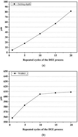
Figure 9.
Variation of the etching depth and width (L2) according to repeated cycles of the DEE process: (a) etching depth and (b) width (L2).
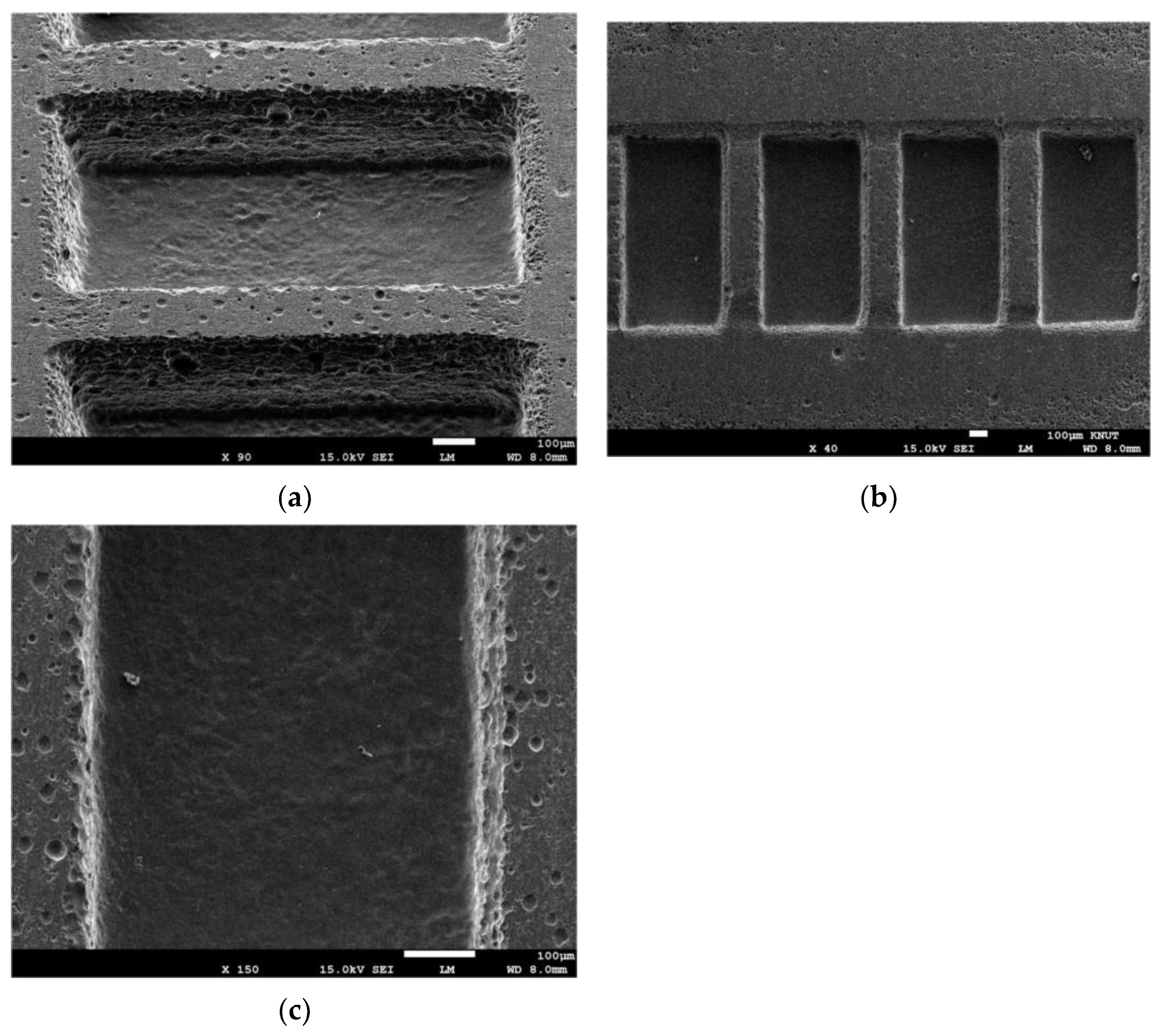
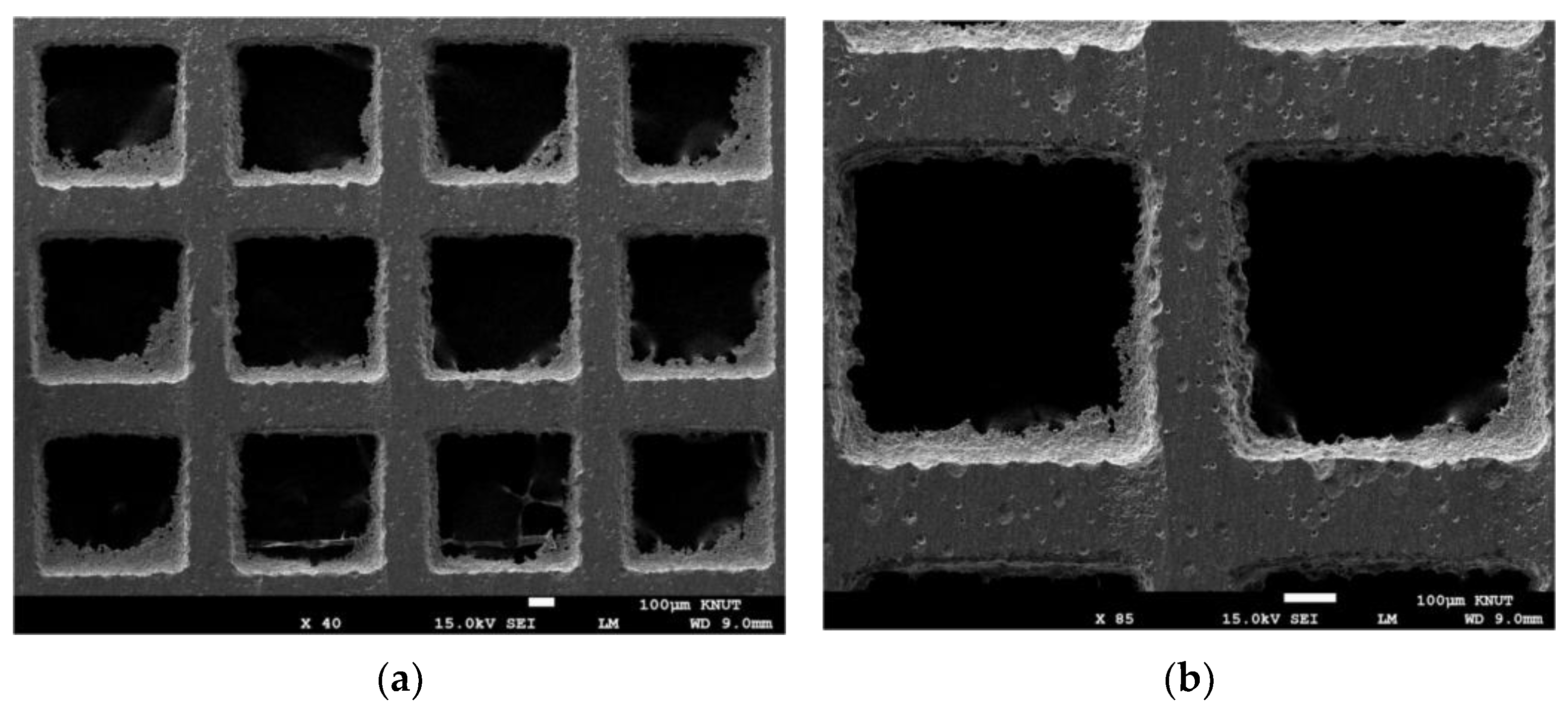
Figure 10 shows the microsquare groove structure fabricated through the DEE process. This microsquare groove structure was obtained by repeating the DEE process cycle 56 times. As a result of measuring the surface profile, it was confirmed that a structural pattern with an etching depth of 220 μm and pitch spacing of 200 μm was successfully fabricated. In addition, the average etching depth per cycle was measured as 3.92 μm. By performing the DEE process on a one-hundred-μm-thick stainless steel specimen, a through-rectangular pattern was successfully fabricated, as shown in Figure 11. Perforated areas from some bottom surfaces were first observed when the number of repeated cycles of the DEE process exceeded 20. As a result of repeating the DEE process cycle up to 27 times in order to reduce the remaining nonpenetrating portion, it can be seen that the remaining nonpenetrated area was reduced, as shown in Figure 11. These results mean not only the blind shape but also the through shape pattern could be implemented through the DEE process.

Figure 10.
Microsquare groove through DEE process: (a) tilted view; (b) top view; (c) magnified view of microsquare groove.
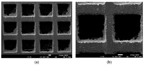
Figure 11.
Penetrating square pattern through DEE process: (a) penetrating square pattern; (b) magnified view of penetrating square.
5. Conclusions
In this study, the DEE process was newly introduced. The DEE process is a process that repeats the three steps of electrodeposition, patterning of the deposited layer by laser beam, and electrochemical etching in one cycle. By using the DEE process, it is possible to process a pattern with a high aspect ratio on metal. For the optimization of the DEE process, conditions for forming a suitable deposited layer thickness, laser beam irradiation conditions for removing the deposited layer, and electrochemical etching conditions were selected. Based on this, the manufacturing characteristics according to the repeated cycles of the DEE process were confirmed. Through this, the depth to be machined in one DEE cycle was selected to be about 4 μm. From these results, shapes having an etch factor far exceeding 1.5, which is the limiting etch factor in the electrochemical etching of metals exhibiting isotropic etching characteristics, were machined. In addition, the precision of the final shape can be adjusted by adjusting the etching depth per cycle of the DEE process. Finally, by using the DEE process, a microstructure pattern with a depth of 220 μm as well as a penetration shape on the surface of one-hundred-μm-thick stainless steel was successfully fabricated. These results mean that, through the DEE process, it is possible to process a pattern shape with a high etch factor such as the DRIE process for metal materials. It is also a result showing the possibility of anisotropic etching in metal.
Funding
This work was supported by the National Research Foundation of Korea (NRF) grant funded by the Korea government (MSIT) (No. 2017R1C1B1005444).
Institutional Review Board Statement
Not applicable.
Informed Consent Statement
Not applicable.
Data Availability Statement
Not applicable.
Conflicts of Interest
The author declares no conflict of interest.
References
- Datta, M.; Landolt, D. Fundamental aspects and applications of electrochemical microfabrication. Electrochim. Acta 2000, 45, 2535–2558. [Google Scholar] [CrossRef]
- Datta, M.; Harris, D. Electrochemical micromachining: An environmentally friendly, high speed processing technology. Electrochim. Acta 1997, 42, 3007–3013. [Google Scholar] [CrossRef]
- Datta, M.; Harris, D. Electrochemical processing technologies in chip fabrication: Challenges and opportunities. Electrochim. Acta 2003, 48, 2975–2985. [Google Scholar] [CrossRef]
- Park, M.S.; Chu, C.N. Micro-electrochemical machining using multiple tool electrodes. J. Micromech. Microeng. 2007, 17, 1451. [Google Scholar] [CrossRef]
- Duan, W.; Mei, X.; Fan, Z.; Li, J.; Wang, K.; Zhang, Y. Electrochemical corrosion assisted laser drilling of micro-hole without recast layer. Optik 2020, 202, 163577. [Google Scholar] [CrossRef]
- Zhang, H.; Xu, J. Laser drilling assisted with jet electrochemical machining for the minimization of recast and spatter. Int. J. Adv. Manuf. Technol. 2012, 62, 1055–1062. [Google Scholar] [CrossRef]
- Zhang, H.; Gao, P.; Xu, J.; Yuan, L. Effect of Electrochemical Dissolving in Laser Drilling Assisted with Jet Electrochemical Machining. Int. J. Electrochem. Sci. 2021, 16, 21056. [Google Scholar] [CrossRef]
- Park, M.S.; Kim, B.S. Fabrication of Glass Microstructure Using Laser-Induced Backside Wet Etching. Trans. KSME A 2014, 38, 967–972. [Google Scholar]
- Shin, H.S.; Chung, D.K.; Park, M.S.; Kim, B.H.; Chu, C.N. Electrochemical etching of stainless steel through laser masking. J. Micromech. Microeng. 2010, 20, 055030. [Google Scholar] [CrossRef]
- Shin, H.S.; Park, M.S.; Chu, C.N. Electrochemical etching using laser masking for multilayered structures on stainless steel. CIRP Ann-Manuf. Technol. 2010, 59, 585–588. [Google Scholar] [CrossRef]
- Chen, X.; Fang, X.L. Reduction of undercutting in electrochemical micro-machining of micro-dimple arrays by utilizing oxygen produced at the anode. Surf. Coat. Technol. 2015, 277, 44–51. [Google Scholar] [CrossRef]
- Parasuraman, J.; Summanwar, A.; Marty, F.; Basset, P.; Angelescue, D.; Bourouina, T. Deep reactive ion etching of sub-micrometer trenches with ultra high aspect ratio. Microelectron. Eng. 2014, 113, 35–39. [Google Scholar] [CrossRef]
- Shin, H.S. E Selective Electrochemical Etching of Stainless Steel Using a Laser-Patterned Copper Layer. Int. J. Precis. Eng. Manuf. 2019, 20, 711–716. [Google Scholar] [CrossRef]

Publisher’s Note: MDPI stays neutral with regard to jurisdictional claims in published maps and institutional affiliations. |
© 2022 by the author. Licensee MDPI, Basel, Switzerland. This article is an open access article distributed under the terms and conditions of the Creative Commons Attribution (CC BY) license (https://creativecommons.org/licenses/by/4.0/).