Article

Preliminary Study on Detecting the Internal Voltage Values of Integrated Circuits Based on Electro-Optical Frequency Mapping

1
National Space Science Center, Chinese Academy of Sciences, Beijing 100190, China
2
School of Astronomy and Space Science, University of Chinese Academy of Sciences, Beijing 100049, China
*
Author to whom correspondence should be addressed.
Appl. Sci. 2022, 12(3), 1188; https://doi.org/10.3390/app12031188
Submission received: 10 January 2022 / Revised: 20 January 2022 / Accepted: 21 January 2022 / Published: 24 January 2022
(This article belongs to the Section Applied Physics General)

Abstract

:
Electro-optical frequency mapping (EOFM) technology can detect node signals from the backside of integrated circuits (ICs). In the past, the detected signal only qualitatively represented the electrical activity strength inside the device. In this paper, the electro-optical signal generation mechanism of the device is systematically studied, and a concise physical model of laser beam modulation based on the optical transmission matrix is proposed. Firstly, the influence of the bandwidth of the laser and each structure covered by the laser spot on the electro-optical signal of the device is well described by the model. Secondly, the model quantifies the electro-optical signal strength, and shows it is positively correlated with the laser wavelength and the reverse bias voltage. Finally, the model is used to quantitatively calculate the accurate voltage level of the internal node inside the device using the detected signal, and the calculation results match well with the experimental results. The model provides theoretical guidance for the efficient and accurate extraction of internal voltage values of devices by EOFM technology.

1. Introduction

The Electro-Optical Frequency Mapping (EOFM) technique, an optical contactless probing, is undeniably powerful in the integrated circuit (IC) failure analysis realm, owing to the applications in distinguishing transistor toggling at a specific frequency through the backside of silicon ICs and reducing electrical failure analysis time [1,2,3,4]. Recently, EOFM has also been treated as a new class of physical attack that is fast becoming a key instrument in the hardware security community [5,6]. Without making any physical contact with ICs, an adversary can probe volatile and on-die-only secret data from the backside of a chip just with the help of an EOFM technique [7,8,9,10]. However, the physical mechanisms of EOFM signals from modern ICs have not been understood completely to date. Although the intensity of electrical activities in each part of the device under test (DUT) can be characterized by the detected EOFM signal, the amplitude of the EOFM signal only represents the device activities qualitatively but not quantitatively. It is worth mentioning that we could analyze and interpret the probed area better with the accurate voltage level of the probed node. Historically, electron beam and mechanical probes were utilized to detect the voltage amplitude of the signal at the point to be probed from the front-side; however, the use of flip-chip packages and the high number of interconnect levels made these probing methods difficult. Additionally, electron beam and mechanical probers are intrusive and require extensive preparatory work [11,12]. As a result, figuring out the connection between the accurate voltage level inside the DUT and the signal of the DUT detected by EOFM is an urgent requirement [11].
In some previous work [13,14,15], researchers explored the EOFM signal generation mechanism of the DUT and proposed several theories on the EOFM signal generation mechanism of the DUT. Existing research confirms that the free carrier effect is one of the major contributors to the EOFM signal generation of the DUT, and also recognizes the critical role played by multiple reflections and absorptions on many different interfaces during the EOFM signal generation. Although some research has been carried out on the EOFM signal generation mechanism of the DUT, there has been little quantitative analysis of the detected EOFM signals. Consequently, up to now, the detailed voltage information of the DUT has still not been obtained from the detected EOFM signal [11]. Additionally, existing studies simply assume that the laser is focused on the metal layer on the front side of the DUT, and the modulated laser is reflected by the metal layer, whose reflectivity is considered to be 98 % . A systematic understanding of the relationship between each elementary part covered by the laser spot and the EOFM signal of the DUT is still lacking.
In this paper, we propose a novel physical model of the EOFM signal of the device based on the existing research. The purpose of this paper is to use the EOFM signal values obtained from experiments to extract detailed voltage information of the DUT through the proposed physical model. The formulas to calculate some of the physical parameters in the model are experimentally modified to match the actual situation better. The model also provides the methodology to calculate the total reflectivity contributed by each elementary part covered by the laser spot. The first section of this paper briefly analyzes the EOFM signal generation mechanism of the DUT and introduces the physical calculation model based on the transfer matrix. Next, an EOFM experiment is carried out on the diode to verify the effectiveness of the model. The above investigation can be a vital guide to extracting the detailed voltage information of the DUT and predicting the scaling of the EOFM signal at future process technologies.

2. Detecting Principle

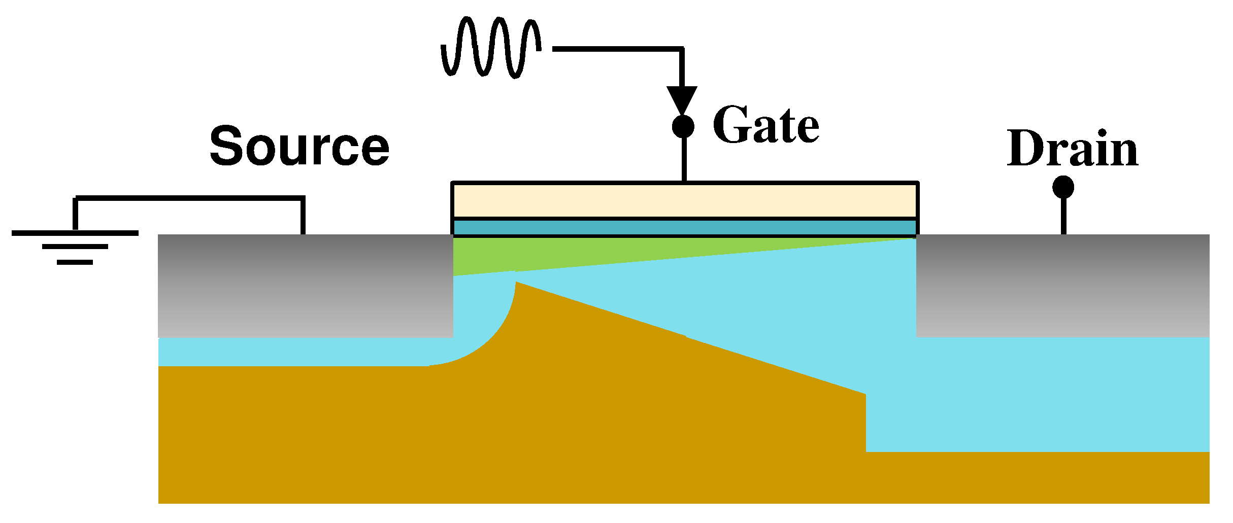
2.1. Principle of EOFM

When the laser beam is focused on the switching transistor, many laser–semiconductor interactions occur. As a result, the phase of the reflected light is modulated at the switching frequency. These phase modulations of the reflected light can be converted into amplitude modulations by interferometric effects. EOFM uses a high-sensitivity photodetector to detect the amplitude modulation of the reflected light in the parts-per-million range, thereby locating the position of the transistor operating at the frequency of interest [12,16,17]. The 1319 nm laser wavelength is widely used in the EOFM, and the main effect of this wavelength is the free carrier effect [11]. The free carrier effect in silicon describes the change in absorption coefficient and refractive index as a function of free carrier density [18]:
n f c = q 2 λ 2 8 π 2 c 2 ε 0 n 0 Δ N e m c e * + Δ N h m c h *
α f c = q 3 λ 2 4 π 2 c 3 ε 0 n 0 Δ N e m c e * 2 μ e + Δ N h m c h * 2 μ h
where n f c and α f c are the changes in refraction index and the absorption coefficient, respectively. q is the elementary charge, λ is the wavelength, ε 0 is the permittivity of free space, n 0 is the refractive index of the unperturbed crystalline silicon, and c is the speed of light in vacuum. Δ N e and Δ N h are, respectively, the change in the electron and hole density; m c e * and m c h * are, respectively, the effective masses of the electron and hole.
Figure 1 shows the cross-section of a metal-oxide-semiconductor field-effect transistor (MOSFET). The drain potential oscillation caused by the gate voltage pattern can result in carrier density perturbations. According to Equations (1) and (2), the refractive index and light absorption of silicon will change due to the presence of free carriers. Therefore, the reflected light is modulated in both amplitude and phase. Previous studies indicate that the EOFM signals of the DUT come from the channel underneath the gate and the space charge region (SCR) underneath the drain [13,14]. If we want to use the signal from the channel to obtain the voltage information of the DUT, the model will be very complicated due to the existence of the inversion charge in the channel. Additional electrical simulations are required to obtain the inversion charge carrier density in the channel. By contrast, the drain signal comes from the SCR thickness variation of the reverse biased junction underneath the drain. The reverse biased junction is a part of every transistor in modern ICs; on the other hand, the electrical model of the reverse biased junction is simple. Because of this, we built a physical model of the reverse biased junction to obtain the accurate voltage level of the DUT through the reverse biased junction signal.

2.2. Theoretical Model

Because the phase modulation of the reflected light is converted to amplitude modulation through interference, a detector was used to detect the optical power of the reflected light in the experiment [16,19]. The optical power of the incident light is known in the experiment, so the EOFM signal of the DUT can also be expressed as
R V p = P r e f P i n c = R 0 + Δ R V p
where R V p is the reflectivity of the DUT, P i n c and P o u t are, respectively, the incident and reflected laser powers, R 0 is the static reflectivity of the DUT without power, and Δ R ( V p ) is the change in reflectivity due to the external voltage on the DUT, namely the EOFM signal of the DUT. Equation (3) shows that the EOFM signal of the DUT is essentially caused by the variation of the reflectivity of the DUT with the applied voltage. Therefore, we only need to build a physical model to calculate the reflectivity of the DUT, and then the corresponding EOFM signal values of the DUT under different voltages can be obtained using the proposed model. The detailed model-building process is given below.
Semiconductor devices usually contain several differently doped regions. In order to provide even greater simplicity for the model, the device is simplified to a multilayer structure consisting of multiple parallel interfaces as depicted in Figure 2 [15,20]. The incident light, E 0 + , is reflected and transmitted at each interface and partially absorbed as it propagates through each layer of the medium. Finally, all reflected light interferes with each other to form the total reflected light, E 0 . The propagation process of the laser in the device is similar to the propagation process of the light in the multilayer film system. Therefore, the transfer matrix method commonly used to study the reflection properties of thin film systems is applied to the model. With this method, it is possible to calculate the total reflectivity R in multilayer structures [15,18].
The optical properties of each layer in Figure 2 are characterized by the thickness d and the complex refractive index n . n can be expressed as follows:
n = n i k
where n is the absolute refraction index of silicon, which consists of the refraction index of intrinsic silicon n 0 and the free carrier term n f c given by Equation (1), and k is the extinction coefficient. n and k are calculated as shown:
n = n 0 + n f c
k = α λ 4 π
where α is the absorption coefficient of silicon, which can be calculated as shown in the following formula:
α = α 0 + α f c
For the absorption coefficient of intrinsic silicon α 0 , we use experimental data on intrinsic silicon from the literature [21]. The refraction index of intrinsic silicon n 0 in Equation (5) is a function of laser wavelength λ and temperature T [22]:
n 0 = ε T + e 3 Δ L T λ 2 0.8948 + 4.3977 × 10 4 T + 7.3835 × 10 8 T 2 0.5
with
ε T = 11.445 + 2.7739 × 10 4 T + 1.705 × 10 6 T 2 8.1347 × 10 10 T 3
Furthermore, for 293 K < T < 1600 K
Δ L T = 0.071 + 1.887 × 10 6 T + 1.934 × 10 9 T 2 4.554 × 10 13 T 3
In this paper, the temperature change caused by the laser thermal effect can be ignored owing to the small laser power. Therefore, we consider the temperature T = 300 K .
Although the free carrier term, α f c , in Equation (7) can be calculated by Equation (2), in some cases the results calculated by Equation (2) deviate from the experimental data. Therefore, a fitting parameter is introduced in Equation (11) to better agree with the experimental values [20].
α f c = 2.2 q 3 λ 2 4 π 2 c 3 ε 0 n 0 Δ N e m c e * 2 μ e + Δ N h m c h * 2 μ h
where μ e and μ h are the electron and hole mobilities, respectively.
The electron and hole mobilities in silicon are a function of the doping concentration and temperature. Many analytical expressions for calculating mobility can be found in the literature. For the calculations in this work, Equations (12) and (13) are used. Some parameters in Equation (12) are modified to make the calculations consistent with the experimental data [20,23]:
μ e = 74 T n 0.57 + 7.2 × 10 8 T 2.33 1.01 + N 4.5 × 10 16 T n 2.4 0.9 T n 0.146
μ h = 54.3 T n 0.57 + 1.36 × 10 8 T 2.33 1 + N 4.5 × 10 16 T n 2.4 0.88 T n 0.146
where T n = T T 300 300 is the normalized temperature, and N is the free carrier’s density.
By using Equations (4)–(13), we can calculate the complex refractive index of each layer in Figure 2. Then E 0 + and E 0 are obtained by the Fresnel coefficient matrix method [24]:
E 0 + E 0 = 1 t 1 t 2 t l + 1 1 ρ 1 ρ 1 1 j = 1 l e i δ j ρ j + 1 e i δ j ρ j + 1 e i δ j e i δ j E l + 1 + 0 = A B C D E l + 1 + 0
where ρ 1 = n 0 n 1 n 0 + n 1 and t 1 = 2 n 0 n 0 + n 1 are the Fresnel coefficients of interface 1, and δ 1 = 2 π λ n 1 d 1 is the phase factor.
In Figure 2, the reflection coefficients ρ of all interfaces except the last one can be calculated by the complex refractive index n . The reflectivity of the last interface in Figure 2 is contributed by each elementary part of the laser spot coverage (see Figure 3), and we can not directly calculate the reflection coefficient ρ l + 1 using the complex refractive index. To solve this problem, we first calculate the reflectivity R c of the last interface, and we use the obtained reflectivity to calculate the reflection coefficient ρ l + 1 . Taking into account the Gaussian distribution of the laser intensity, the reflectivity of the last interface is expressed as the sum of the reflectivity of each part of the laser coverage multiplied by the Gaussian distribution profile of the laser intensity and the ratio of each part area to the laser spot area:
R c = j = 1 H R j 2 e 2 S j e 2 1 π 2 ω 0 4 x 1 j , y 1 j x 2 j , y 2 j e 2 x j 2 + y j 2 ω 0 2 d x d y
where H is the total number of structures covered by the laser beam, S j is the area of each part, x 1 j , y 1 j and x 2 j , y 2 j are the spatial coordinates of each part, and ω 0 is the spot radius of the focused laser.
After R c is obtained by Equation (15), the reflection coefficient ρ l + 1 at the last interface in Figure 2 can be calculated as shown in the following formula:
ρ l + 1 = R c
All the parameters in Equation (14) are now given in detail, so the total reflection coefficient ρ of the multilayer system in Figure 2 can be obtained through Equation (14):
ρ = E 0 + E 0 = C A
Therefore, the total reflectivity R of the multilayer system is
R = ρ 2
The above analysis process neglects the spectral line width of the laser, which should be taken into account when using the transfer matrix [25]. To make the model calculation results better match with the experimental data, the reflectivity calculated with Equation (18) should be multiplied by the spectral line function g ( λ , λ 0 ) of the laser and then integrated, as written in Equation (19).
R λ 0 , V p = g λ , λ 0 R λ d λ
where λ 0 is the central wavelength.
A semiconductor laser was used in our experimental setup; hence, the spectral line function g ( λ , λ 0 ) of the laser was the Lorentzian function:
g λ , λ 0 = Δ λ 2 π λ 1 λ 2 λ 2 · 1 1 λ 1 λ 0 2 + 1 4 Δ λ λ 1 λ 2 2
λ 1 = λ 0 + Δ λ 2
λ 2 = λ 0 Δ λ 2
where Δ λ is the bandwidth of the laser.
It is worth noting that the parameter used to calculate the EOFM signal is the reflectivity variation Δ R λ 0 , V p rather than the reflectivity itself; Δ R λ 0 , V p is calculated as shown in the following formula:
Δ R λ 0 , V p = R λ 0 , V p R λ 0 , 0
where R λ 0 , V p is the reflectivity obtained for a voltage level V p , and R λ 0 , 0 is the reflectivity obtained when there is no voltage applied.
In the experiment, the modulated reflected light was converted into a modulating electrical signal by a photodetector. To directly compare the calculation results with the experimental results, Δ R is converted into the experimentally measurable voltage value according to the following equation:
V o u t = · G · P · Δ R
where V o u t is the output signal level of the photodetector, is the responsivity of the photodetector, G is the transimpedance gain of the photodetector, and P is the incident light power.

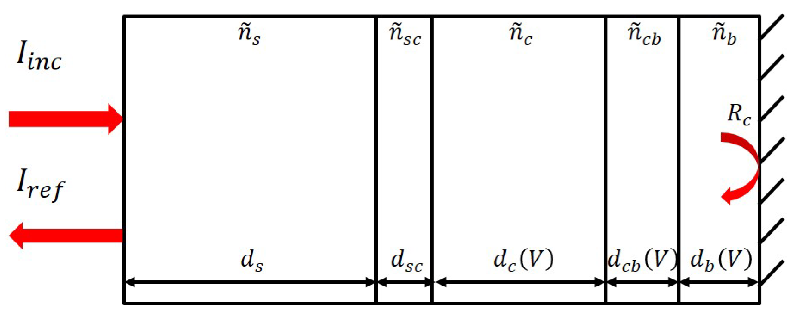
3. Analytical Calculation of the EOFM Signal on the Diode

Using all previous equations, we can now calculate the EOFM signal of a P + N junction at 300 K . Considering the wide application of the 1319 nm laser wavelength in the industry [11], we also used a 1319 nm laser wavelength in our calculations. The bandwidth Δ λ = 2 nm of the laser source used in the experiment was also taken into account in our calculations. The calculated structure was a diode between the base and collector regions of the transistor Q 1 in the CA3083 chip from Intersil. The relative parameters of the diode can be found in the literature [26]. For the reverse biased junction, the device was modeled with five layers as depicted in Figure 4. In Figure 4, the reverse biased diode is simplified to a structure with six interfaces, which are the air/substrate, substrate/SCR, SCR/collector, collector/SCR, SCR/base, and base/contact.
During the modeling process, the P + N junction was treated as an abrupt junction, where the SCR was completely depleted (depletion approximation). The SCR thickness between base and collector depends on the applied voltage; consequently, the different reflectivity values of the DUT can be obtained if the different voltage levels are applied. Additionally, the average doping distribution substituted for the actual doping distribution in this model. The average of the base region ( P + -type) doping concentration was set to 5.279 × 10 17 cm 3 , the collector region (N-type) doping concentration was set to 3.141 × 10 14 cm 3 , and the substrate (P-type) doping concentration was set to 6.054 × 10 12 cm 3 . At the last interface, the reflectivity R c was calculated using Equation (15).
Figure 5 gives the reflectivity variation Δ R of the device as a function of the laser wavelength when the applied voltage V p = 4 V . The signal in Figure 5 is defined as the relative reflectivity variation, Δ R Δ R R 0 R 0 , expressed in parts per million (ppm), because the reflectivity variation value is very weak. This is also the reason why the EOFM signal of the device is very difficult to detect and requires special techniques in signal processing [27]. From Figure 5, the reflectivity variation, i.e., the EOFM signal, increases with the increase in laser wavelength. This is consistent with the phenomenon found in the experiment [14]. The calculation results in Figure 5 show why the 1319 nm laser wavelength is widely utilized in the industry [11].
The EOFM signal V o u t of the diode calculated for different reverse bias voltages applied is shown in Figure 6. When calculating V o u t using Equation (24), the incident light power P was considered to be 11.48 mW, and the parameters of the detector used in the experiment were also employed. The responsivity of the photodiode was set to 0.85 A A W W , and the transimpedance gain G of the photodiode was set to 2.38 × 10 3 V V A A . We can see from Figure 6 that the EOFM signal of the diode increases with the value of the reverse bias voltage. This is caused by the fact that the SCR thickness increases with the applied reverse bias voltage.

4. EOFM Experiment on the Diode and Discussion

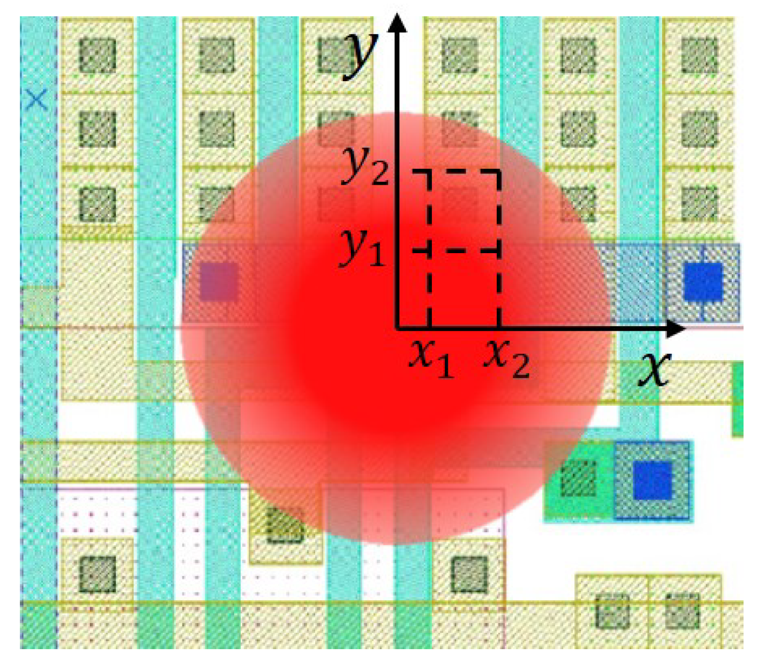
4.1. Experimental Setup
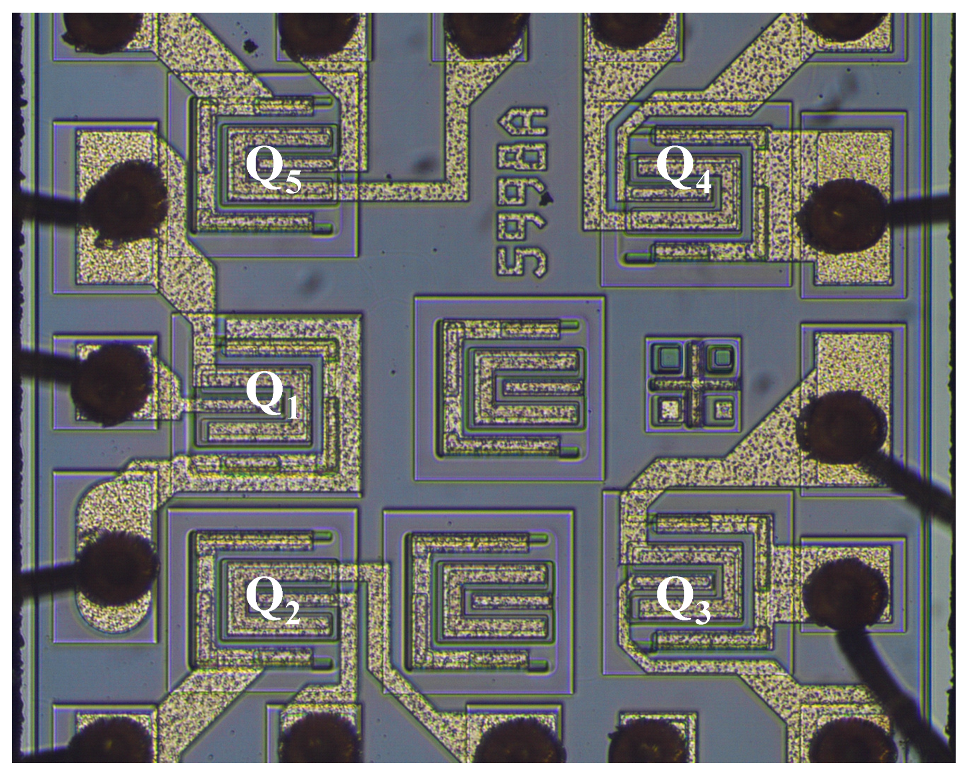
To verify the calculation data, an EOFM experiment was performed on the diode. The equipment we used was the Laser Scanning and Mapping System at the National Space Science Center, Chinese Academy of Sciences. As shown in Figure 7, the experimental setup was composed of an optical system and electrical system. The laser source provided a continuous beam at a wavelength of 1319 nm. After the laser passed through the objective lens, the spot diameter inside the DUT was about 1 um. The laser was focused on the active region of the DUT using a visible light camera. The incident light power on the DUT was about 11.48 mW. A photodiode was used to measure the reflected light power. The photodiode was plugged into the spectrum analyzer to analyze the characteristics of the frequency domain signal from the DUT. The spectrum analyzer received the modulated electrical signal and output the EOFM signal strength at the frequency of interest [17]. The stepper motor controller controlled the XYZ translation stage to move the DUT. A waveform generator was utilized to drive the DUT. The computer controlled the spectrum analyzer, waveform generator, and stepper motor controller via the general-purpose interface bus (GPIB) to automate the experiment. A detailed description of the experimental setup can be found in [28].

4.2. DUT

The DUT is the CA3083 chip mentioned in the simulation. Figure 8 shows the front view of the chip, and each chip includes five independent NPN transistors. We chose the P + N junction between the base and collector regions of the transistor Q 1 as the test structure. The package on the backside of the DUT was opened to facilitate laser back irradiation experiments. During the experiments, the P + N junction was always in reverse bias state. The P + N junction was pulsed with a square wave of 10 kHz frequency, duty cycle of 50 % , and different voltage amplitudes.

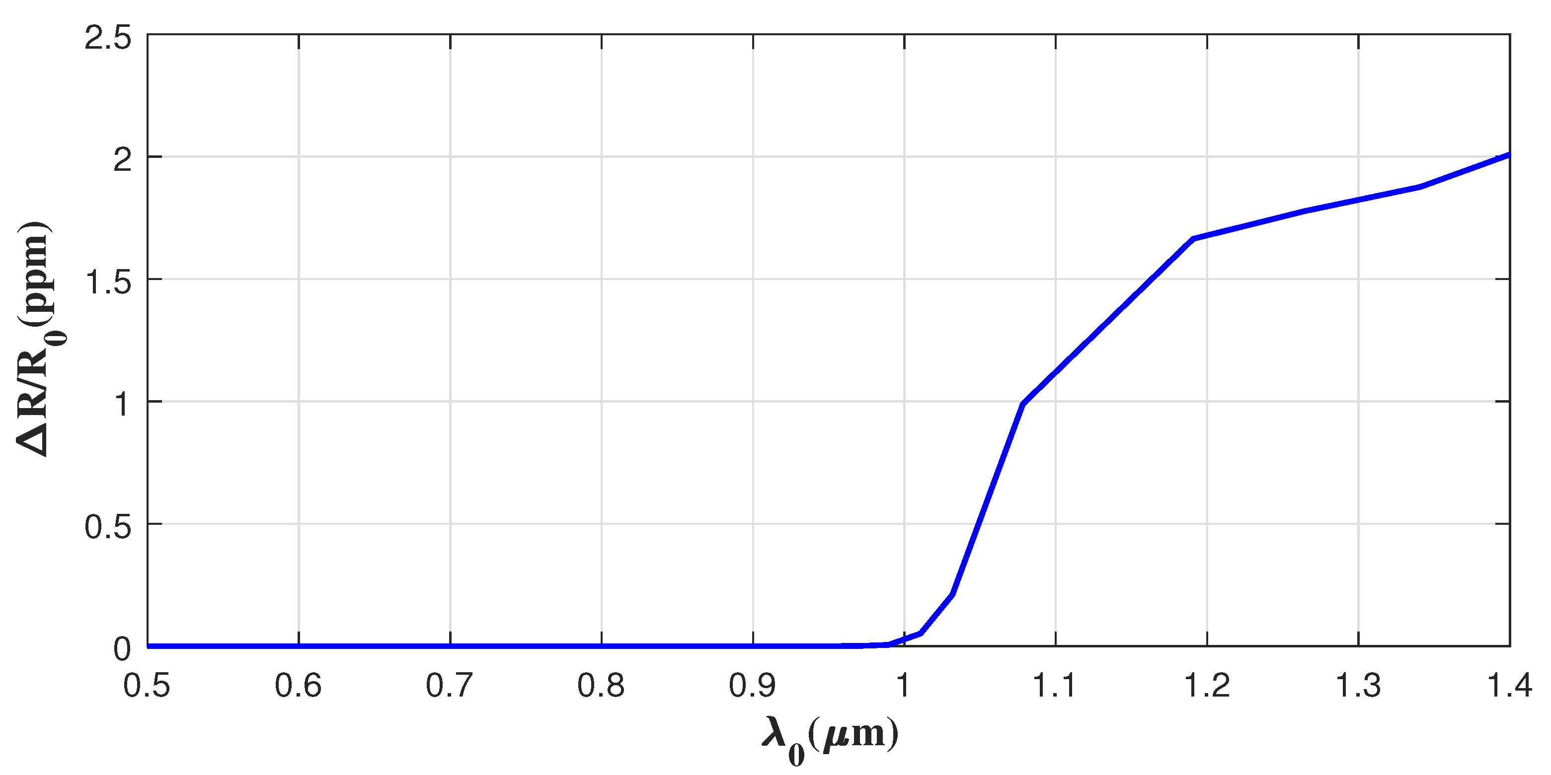
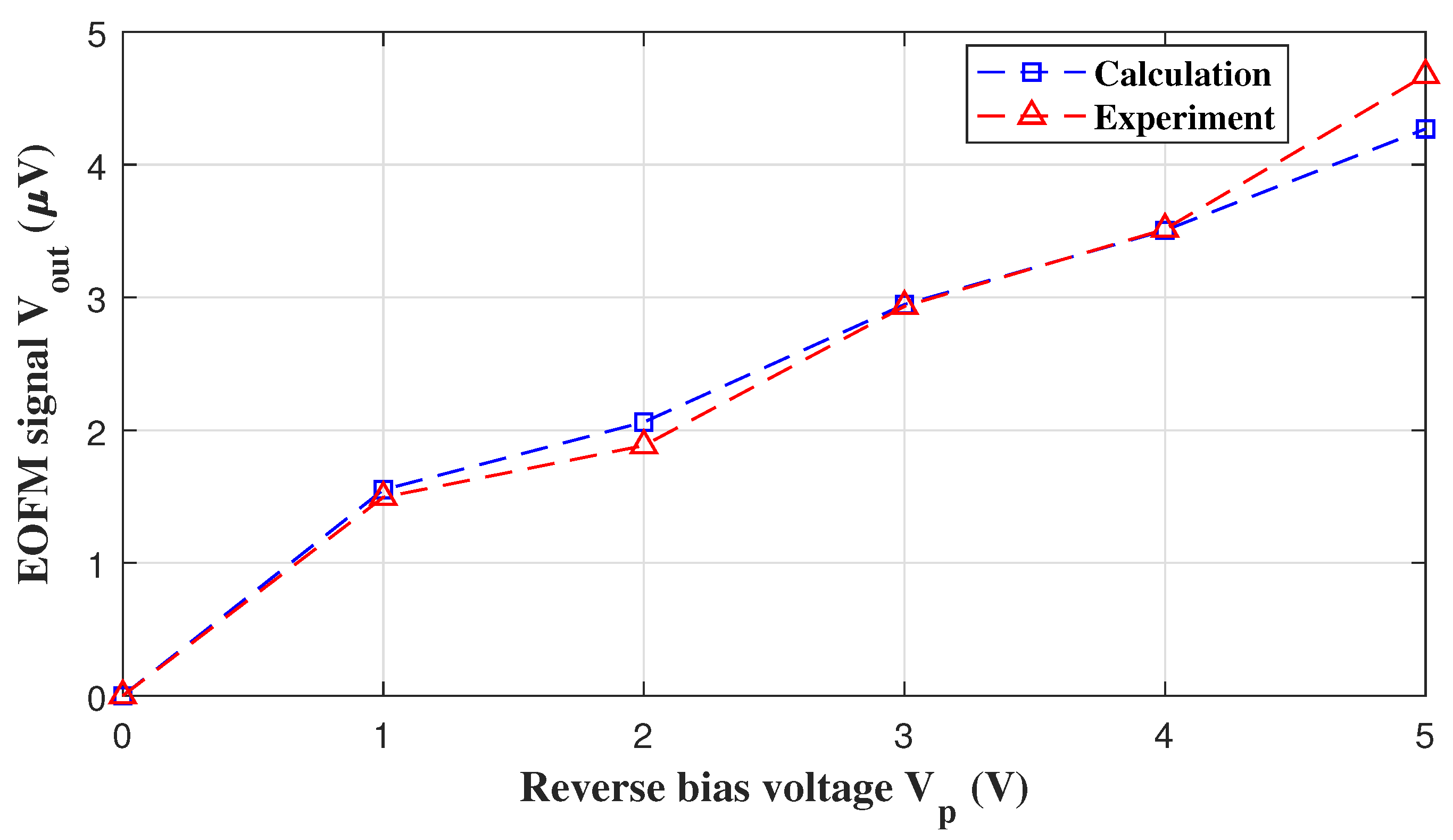
4.3. Experimental Results and Discussion

The maximum EOFM signal at the beginning of the measurement was acquired for a 337 um depth. To ensure the reliability of the experiment, this depth was set for each measurement on the CA3083. The resolution bandwidth of the spectrum analyzer was set to 1 Hz, and the center frequency was 100 kHz with a span of 100 Hz. The peak signal amplitude V o u t at each driving voltage V p was recorded. To directly compare the experimental results and the calculation results, the calculation data in Figure 6 and the experimental data are plotted in Figure 9.
From the data in Figure 9, it is apparent that the measured EOFM signal showed the same dependency on the voltage as predicted in the calculations. We see in Figure 9 that the experimental results agreed well with the calculations. Since we could not obtain the detailed parameters of the DUT from the manufacturer, the parameters of the DUT used in the calculation were obtained from the electrical parameters of the DUT by the semiconductor device simulation software. Therefore, the parameter values of the DUT used in the calculation had deviations from the actual parameter values. If the actual parameter values of the DUT were available in the calculation, the accuracy of the calculation results would be improved. In general, these results still indicate a good validity of our model.

5. Conclusions

To overcome the challenge of calculating the precise voltage level inside the device quantitatively, a concise and effective theoretical model of the EOFM signal of the device was proposed in this paper. This model was established by considering the multibeam interference effect and the free carrier effect when the laser propagates in the device. In addition, the bandwidth of the laser and contribution of each elementary part covered by the laser spot to the total reflectivity were both taken into account in the model; meanwhile, the corresponding calculation methods were also given. Our calculation results show that a long-wavelength laser is beneficial to the detection of the EOFM signal, and the EOFM signal strength increases with the increase in the working voltage. The EOFM signal values obtained from the calculation matched well with the experiment; thus, it is possible to obtain the detailed voltage information in the device by the model.

Author Contributions

Conceptualization, P.L., Y.M. and J.H.; methodology, P.L.; validation, P.L., Y.M. and J.H.; formal analysis, P.L.; investigation, P.L.; resources, Y.M. and J.H.; writing—original draft preparation, P.L.; writing—review and editing, P.L. and Y.M.; visualization, P.L.; supervision, J.H.; project administration, Y.M. and J.H.; funding acquisition, Y.M. All authors have read and agreed to the published version of the manuscript.

Funding

This work was supported by a Grant from the Foundation for Study Encouragement to Youth Innovation Promotion Association Member of Chinese Academy of Sciences, Chinese Academy of Sciences, China (Grant No.2018179 ) and Research and Development Plan Projects in Key Area of Guangdong Province (Grant No.2020B010170001).

Institutional Review Board Statement

Not applicable.

Informed Consent Statement

Not applicable.

Data Availability Statement

The data used to support the findings of this study are available from the corresponding author upon request.

Conflicts of Interest

The authors declare no conflict of interest.

References

  1. Herfurth, N.; Amini, E.; Beyreuther, A.; Nakamura, T.; Keil, S.; Boit, C. EOFM for contactless parameter extraction of low k dielectric MIS structures. In Proceedings of the 2019 IEEE 26th International Symposium on Physical and Failure Analysis of Integrated Circuits (IPFA), Hangzhou, China, 2–5 July 2019; pp. 1–5. [Google Scholar] [CrossRef]
  2. Li, A.; Xiao, R.; Guo, M.; Li, J.; Liu, B. Case Study on Abnormal Electron-Optical Frequency Mapping phenomena in Failure Analysis. In Proceedings of the ISTFA 2018: Proceedings from the 44th International Symposium for Testing and Failure Analysis, Phoenix, AZ, USA, 28 October–1 November 2018; pp. 156–160. [Google Scholar] [CrossRef]
  3. Sheng, F.L.; Ling, L.J. Application of electro optical frequency mapping (EOFM) in scan chain failure analysis for ASIC. In Proceedings of the 2017 IEEE 24th International Symposium on the Physical and Failure Analysis of Integrated Circuits (IPFA), Chengdu, China, 4–7 July 2017; pp. 1–5. [Google Scholar] [CrossRef]
  4. Rebaï, M.M.; Darracq, F.; Guillet, J.P.; Bernou, E.; Sanchez, K.; Perdu, P.; Lewis, D. A comprehensive study of the application of the EOP techniques on bipolar devices. Microelectron. Reliab. 2014, 54, 2088–2092. [Google Scholar] [CrossRef]
  5. Kiyan, T.; Lohrke, H.; Boit, C. Comparative Assessment of Optical Techniques for Semi-Invasive SRAM Data Read-out on an MSP430 Microcontroller. In Proceedings of the ISTFA 2018: Proceedings from the 44th International Symposium for Testing and Failure Analysis, Phoenix, AZ, USA, 28 October–1 November 2018; p. 266. [Google Scholar] [CrossRef]
  6. Jain, A.; Zhou, Z.; Guin, U. Survey of Recent Developments for Hardware Trojan Detection. In Proceedings of the 2021 IEEE International Symposium on Circuits and Systems (ISCAS), Daegu, Korea, 22–28 May 2021; pp. 1–5. [Google Scholar] [CrossRef]
  7. Boit, C.; Kiyan, T.; Krachenfels, T.; Seifert, J.P. Logic State Imaging From FA Techniques for Special Applications to One of the Most Powerful Hardware Security Side-Channel Threats. In Proceedings of the 2020 IEEE International Symposium on the Physical and Failure Analysis of Integrated Circuits (IPFA), Singapore, 20–23 July 2020; pp. 1–7. [Google Scholar] [CrossRef]
  8. Lohrke, H.; Tajik, S.; Boit, C.; Seifert, J.P. No place to hide: Contactless probing of secret data on FPGAs. In Proceedings of the International Conference on Cryptographic Hardware and Embedded Systems, Santa Barbara, CA, USA, 17–19 August 2016; Springer: Berlin/Heidelberg, Germany, 2016; pp. 147–167. [Google Scholar] [CrossRef]
  9. Tajik, S.; Lohrke, H.; Seifert, J.P.; Boit, C. On the power of optical contactless probing: Attacking bitstream encryption of FPGAs. In Proceedings of the 2017 ACM SIGSAC Conference on Computer and Communications Security, Dallas, TX, USA, 30 October–3 November 2017; pp. 1661–1674. [Google Scholar] [CrossRef]
  10. Lavdas, L.; Rahman, M.T.; Tehranipoor, M.; Asadizanjani, N. On Optical Attacks Making Logic Obfuscation Fragile. In Proceedings of the 2020 IEEE International Test Conference in Asia (ITC-Asia), Taipei, Taiwan, 23–25 September 2020; pp. 71–76. [Google Scholar] [CrossRef]
  11. Kindereit, U. Fundamentals and future applications of Laser Voltage Probing. In Proceedings of the 2014 IEEE International Reliability Physics Symposium, Waikoloa, HI, USA, 1–5 June 2014. [Google Scholar] [CrossRef]
  12. Serrels, K.A.; Ganesh, U. Laser Voltage Probing of Integrated Circuits: Implementation and Impact. In Microelectronics Fialure Analysis Desk Reference; ASM International: Almere, The Netherlands, 2019; p. 244. [Google Scholar] [CrossRef]
  13. Kindereit, U.; Woods, G.; Tian, J.; Kerst, U.; Leihkauf, R.; Boit, C. Quantitative investigation of laser beam modulation in electrically active devices as used in laser voltage probing. IEEE Trans. Device Mater. Reliab. 2007, 7, 19–30. [Google Scholar] [CrossRef]
  14. Pagano, C.; Boit, C.; Glowacki, A.; Leihkauf, R.; Yokoyama, Y. Comparison of FET electro-optical modulation for 1300 nm and 1064 nm laser sources. Microelectron. Reliab. 2012, 52, 2024–2030. [Google Scholar] [CrossRef]
  15. Vogt, I.; Leihkauf, R.; Nakamura, T.; Boit, C. New Laser Voltage Signal Insights from EOFM Simulations and Measurements on different pn-junctions. In Proceedings of the 2018 IEEE International Symposium on the Physical and Failure Analysis of Integrated Circuits (IPFA), Singapore, 16–19 July 2018; pp. 1–6. [Google Scholar] [CrossRef]
  16. Lo, W.; Nataraj, N.; Boiadjieva, N.; Vedegarbha, P.; Wilsher, K. Polarization difference probing: A new phase detection scheme for laser voltage probing. In Proceedings of the ISTFA 2004, Worcester, MA, USA, 14–18 November 2004; ASM International: Almere, The Netherlands, 2004; pp. 9–17. [Google Scholar] [CrossRef]
  17. Ng, Y.S.; Lundquist, T.; Skvortsov, D.; Liao, J.; Kasapi, S.; Marks, H. Laser voltage imaging: A new perspective of laser voltage probing. In Proceedings of the 36th International Symposium for Testing and Failure Analysis, Addison, TX, USA, 14–18 November 2010; pp. 5–13. [Google Scholar] [CrossRef]
  18. Soref, R.; Bennett, B. Electrooptical effects in silicon. IEEE J. Quantum Electron. 1987, 23, 123–129. [Google Scholar] [CrossRef] [Green Version]
  19. Wilsher, K.; Lo, W.; Eiles, T.M.; Xiao, G. Integrated circuit waveform probing using optical phase shift detection. In Proceedings of the ISTFA 2000, Bellevue, WA, USA, 12–16 November 2000; ASM International: Almere, The Netherlands, 2000; pp. 479–485. [Google Scholar] [CrossRef]
  20. Rebai, M.M.; Darracq, F.; Lewis, D.; Perdu, P.; Sanchez, K. How to interpret the reflected laser probe signal of multiple elementary substructures in very deep submicron technologies. In Proceedings of the 39th International Symposium for Testing and Failure Analysis (ISTFA 2013), San Jose, CA, USA, 3–7 November 2013; pp. 471–481. [Google Scholar] [CrossRef]
  21. Green, M.A. Self-consistent optical parameters of intrinsic silicon at 300 K including temperature coefficients. Sol. Energy Mater. Sol. Cells 2008, 92, 1305–1310. [Google Scholar] [CrossRef]
  22. Li, H. Refractive index of silicon and germanium and its wavelength and temperature derivatives. J. Phys. Chem. Ref. Data 1980, 9, 561–658. [Google Scholar] [CrossRef]
  23. Arora, N.D.; Hauser, J.R.; Roulston, D.J. Electron and hole mobilities in silicon as a function of concentration and temperature. IEEE Trans. Electron Devices 1982, 29, 292–295. [Google Scholar] [CrossRef]
  24. Yan, J.; Wei, G.; Ha, L.; Lin, Y.; Jiang, X. Matrix Optical; China North Industries Group Corporation Limited: Beijing, China, 1995. [Google Scholar]
  25. Boit, C.; Glowacki, A.; Pagano, C.; Kerst, U.; Yokoyama, Y. Quantitative aspects of optical IC debug using state-of-the-art backside preparation. In Proceedings of the 2012 19th IEEE International Symposium on the Physical and Failure Analysis of Integrated Circuits, Singapore, 2–6 July 2012; pp. 1–6. [Google Scholar] [CrossRef]
  26. Rebaï, M.M. Integrated Circuit Analysis by Laser Probing Techniques. Ph.D. Thesis, University of Bordeaux, Bordeaux, France, 2014. [Google Scholar]
  27. Boscaro, A.; Jacquir, S.; Sanchez, K.; Perdu, P.; Binczak, S. Improvement of signal to noise ratio in electro optical probing technique by wavelets filtering. Microelectron. Reliab. 2015, 55, 1585–1591. [Google Scholar] [CrossRef] [Green Version]
  28. Liu, P.; Han, J.; Ma, Y.; Zhang, F.; Wu, Z.; Zhu, X.; Cui, Y. A frequency mapping method for locating functional units inside ICs based on coaxial microscope. Electron. Lett. 2021. [Google Scholar] [CrossRef]
Figure 1. Cross-sectional diagram of MOSFET.
Applsci 12 01188 g001
Figure 2. Schematic of the multilayer system. E 0 + is the electricity vector of the incident light, and E 0 is the electricity vector of the reflected light.
Applsci 12 01188 g002
Figure 3. Illustration of the laser spot covering many elementary parts.
Applsci 12 01188 g003
Figure 4. Simplified reverse biased diode structure for the calculation.
Applsci 12 01188 g004
Figure 5. Relative reflectivity variation Δ R Δ R R 0 R 0 for V p = 4 V , considering the bandwidth of the laser Δ λ = 2 nm.
Applsci 12 01188 g005
Figure 6. EOFM signal Δ R calculated for different voltages applied.
Applsci 12 01188 g006
Figure 7. Schematic diagram of the Laser Scanning and Mapping System.
Applsci 12 01188 g007
Figure 8. Front side view of the chip.
Applsci 12 01188 g008
Figure 9. EOFM signal level obtained by calculation and experiment.
Applsci 12 01188 g009
Publisher’s Note: MDPI stays neutral with regard to jurisdictional claims in published maps and institutional affiliations.

