1. Introduction
The development of semiconductor processing has been dictated by Moore’s law over the past 50 years, and the size of a typical metal-oxide-semiconductor field-effect transistor (MOSFET) device will be reduced to 2 nm by EUV photolithography by 2024 [
1,
2]. To be precise, the term “2 nanometer” is not associated with the precise physical feature of a typical transistor, but is a commercial term utilized by the chip manufacturing industry based on transistor density, operational speed, and power consumption [
3]. As the device size decreases, MOS devices with multi-gate structures are increasingly employed for integrated circuits, including FinFET [
4], gate-all-around (GAA) [
5,
6], and nanosheet-based three-dimensional devices [
7,
8]. Additionally, various semiconductor materials have been utilized for high-performance semiconductor devices, including high-k hafnium oxide and 2D semiconductor materials [
9,
10], etc. Metrology techniques to measure film thickness in a few nanometers, as well as profiling film materials with precise spatial resolution, are highly desirable in the semiconductor fabrication process.
Metrology instruments should be simple to use and accurately calibrated for in-line semiconductor production processes on a nanometer scale with high levels of precision and reliability. The three-dimensional structures of a semiconductor device can be measured using a variety of existing metrology techniques, including 3D optical profilometry, atomic force microscopy (AFM), and scanning electron microscopy (SEM) [
11,
12,
13,
14,
15,
16]. For the surface chemistry of a material film, various techniques have been widely used for academic applications, including Fourier transfer infrared spectroscopy (FT-IR) to measure the chemical bonds of surface molecules and ellipsometry for the investigation of surface optical properties. Most of the analytical techniques are performed over a large area of the film, and local material information on the film is very challenging to gather with a thickness on the order of several nanometers, requiring very surface-sensitive techniques with mapping analysis capability. Auger electron microscopy (AES) and X-ray photoelectron spectroscopy (XPS) are ideal candidate metrology techniques for semiconductor processing [
17,
18,
19]. Auger electron microscopy (AES) is performed by bombarding a sample surface with a precisely focused electron beam, which induces the emission of secondary electrons and Auger electrons from the sample surface. Then, an Auger analyzer is utilized to measure the exact mass and intensity of the Auger electron peaks, and the exact identity of an element or molecular fragments can be verified. For X-ray photoelectron spectroscopy (XPS), the sample surface is exposed to a focused X-ray beam with a particular wavelength, the kinetic energies of the emitted electrons are measured, and the electron binding energy of each emitted electron is determined using the photoelectric effect equation. AES can achieve a spatial resolution of up to 7 nm, while XPS can achieve spatial resolution of as small as 5 microns, which is quite suitable to analyze an extraordinarily thin film in a two-dimensional (2D) and three-dimensional (3D) manner [
18]. However, the transition of the AES and XPS techniques into a metrology platform for the semiconductor fabrication process is not an easy task, and a high-quality calibration sample should be fabricated with high uniformity.
Self-assembled monolayer (SAM) based micro and nanostructures could be ideal devices to evaluate advanced semiconductor fabrication and characterization equipment for the AES and XPS techniques. A SAM film is a highly ordered molecular assembly formed by a spontaneous chemical reaction between a SAM precursor and the solid surface underneath [
20,
21]. The SAM precursor is composed of three components: a head group, a carbon chain skeleton, and a tail group. The head group and a tail group can be tailor-designed for specific applications, which makes SAM materials an excellent ecosystem for micro/nano surface property modification. During the chemical reaction between the tail group and the solid surface underneath, the monolayer will spontaneously pack into a highly ordered film due to the van der Waals forces between the carbon chain skeleton of the SAM precursor. Similarly to the head groups, the tail group also can be selected among various chemical groups catering to the specific solid surface underneath, including a thiol group (-SH) on a gold surface [
22,
23] or trichlorosilanes (-SiCl
3) and trimethoxysilanes (-Si (OCH
3)
3) on an oxide surface [
24]. In particular, trichlorosilanes are intensively investigated in semiconductor-related applications to modify a dielectric layer’s surface properties, including those of silicon oxide, aluminum oxide, and ITO [
24,
25,
26]. There are two categories of techniques to fabricate SAM films; liquid-based methods are one, and vapor-based methods are the other. For liquid-based methods, high-quality SAM films from trichlorosilane precursors are laborious to make because the amount of water in the SAM precursor solution needs to be meticulously controlled [
19,
20]. Absent or low amounts of water in the SAM precursor solution will result in incomplete SAM film formation. On the contrary, too much water will lead to facile polymerization of the SAM precursor in solution and unwanted polysiloxane deposition on the solid surface underneath. Typically, there are many defects in the SAM films obtained from the liquid-based methods [
21,
22]. Therefore, several vapor-based methods have been developed to make SAM films in an ambient environment or in a vacuum chamber [
23,
24,
25]. For instance, the hexa-methyl-disilazane (HMDS) layer obtained in a vacuum chamber—a regular process in a high-end semiconductor facility—has the smallest number of surface defects. For the vapor-based deposition method, the liquid formed SAM precursor and catalyst will be vaporized due to the low vacuum condition and be transferred to a vacuum chamber at a specific temperature. The amount of HMDS precursor vapor will be precisely controlled by a flow meter. With no contaminants from the ambient environment and precise reaction process control, a high-quality HMDS SAM film can be obtained with fewer physical defects and higher uniformity. To be qualified as a calibration sample for the AES and XPS techniques, highly uniform SAM-based micro/nanostructures with fewer physical defects must be fabricated.
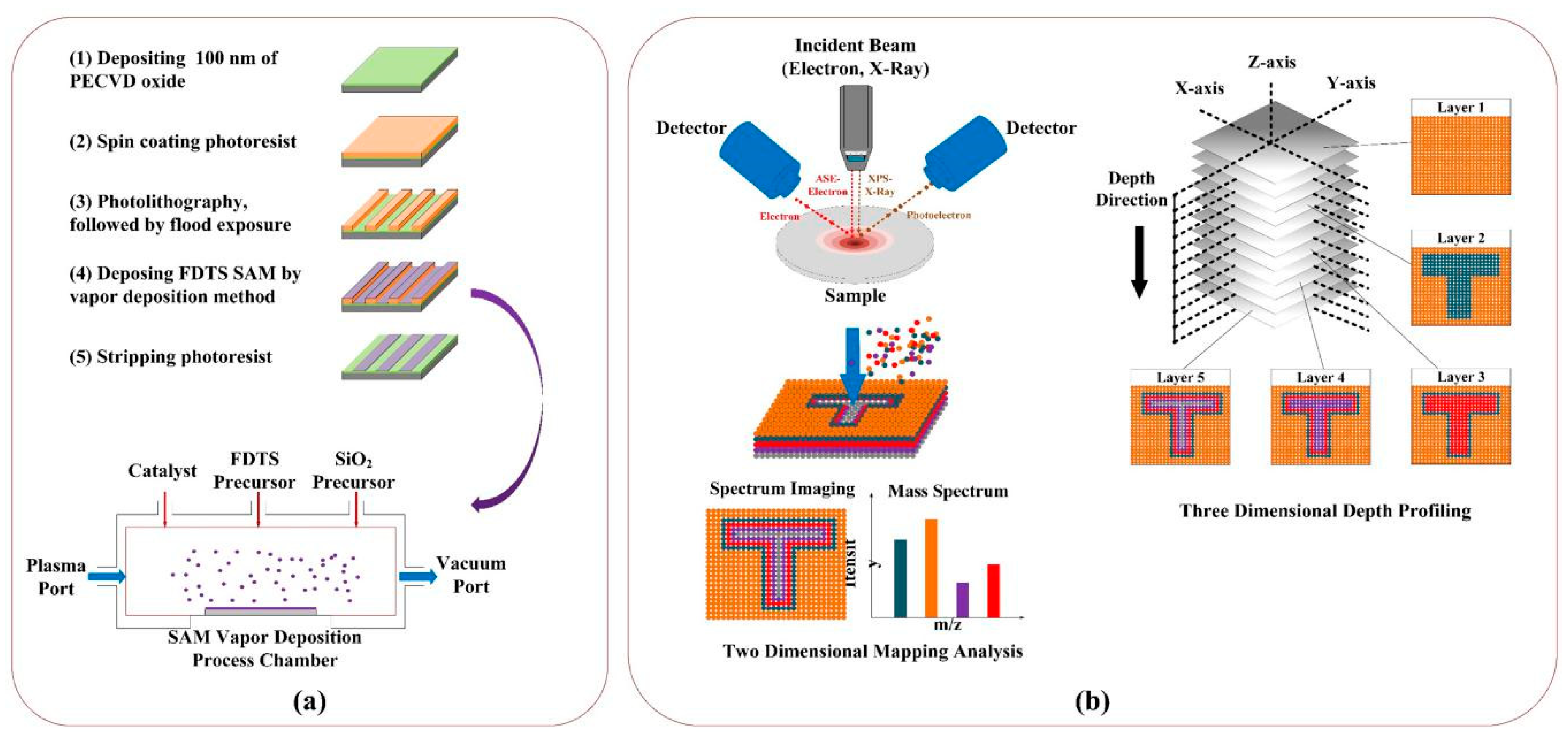
In this paper, precise SAM patterns in micrometer scale were fabricated by several conventional semiconductor fabrication techniques combined, including photolithography, SAM vapor deposition, and a lift-off technique using trichlorosilane (1H,1H,2H,2H-perfluorodecyltrichlorosilane, FDTS). The FDTS SAM film patterns were characterized by Auger electron spectroscopy (AES) and X-ray photoelectron spectroscopy (XPS), both of which have mapping analysis capabilities. AES is a highly surface-sensitive analytical technique involving the bombardment of the FDTS SAM film pattern surface with low-energy incident electrons from 50 eV to 3.0 keV [
17]. The related elements of KLL Auger electrons on the FDTS SAM film pattern surface are then collected and analyzed to evaluate FDTS SAM film pattern quality based on these elements, especially the element fluorine. Meanwhile, X-ray photoelectron spectroscopy (XPS) is also conducted to characterize the FDTS SAM film patterns with a mapping analysis capability. For XPS analysis, lower-energy incident X-rays of about 1 keV bombard the FDTS SAM film pattern surface, and the induced low-energy photoelectrons are ejected from the core shells of the atoms within the FDTS SAM film patterns. Those electrons are then collected and dispersed in an analyzer. Through measuring the kinetic energies of the induced photoelectrons entering the analyzer, the binding energies of different chemical states of the FDTS SAM film patterns are calculated and scanned. AES and XPS are complementary surface-sensitive techniques: one with superior spatial resolution and the other more versatile for chemical state analysis. By incorporating these two surface-sensitive techniques, comprehensive information about the FDTS SAM film pattern surface properties is gathered. Precise two-dimensional (2D) FDTS SAM film patterns were reconstructed through fluorine Auger electrons and X-ray stimulated electrons. Additionally, three-dimensional (3D) FDTS SAM film patterns were analyzed layer by layer through XPS mapping analysis. It was also verified that FDTS SAM patterns based on the vapor deposition technique are highly precise and uniform. Meanwhile, SAM-based microstructures produced by the vapor-based method served as excellent samples to evaluate the analytical capabilities of the AES and XPS techniques in measuring a film’s thickness in a few nanometers, as well as the material profile of the film. In the future, AES and XPS techniques could be used as a metrology technique in the semiconductor process with high-quality SAM micro and nanostructures.
2. Materials and Methods
2.1. Photolithography Process
The microfabrication process for FDTS SAM film patterns has been mentioned before. Briefly, the fabrication is shown in
Figure 1a. First, a 100 nm thick silicon dioxide layer was deposited on a 3-inch silicon wafer at 130 °C using a plasma-enhanced chemical vapor deposition (PECVD) technique. Then, a 2.2 µm thick positive photoresist film (Shipley 1818, Shipley Company Inc., Marlborough, MA, USA) was spin-coated on the silicon wafer surface at 3000 rpm for 30 s. After soft baking for 60 s at 90 °C, the photoresist was exposed with a contact aligner (EV 620, E.V. Group Inc., Hillsboro, OR, USA) for 6.4 s with an exposure dose of 76.8 mJ/cm
2. Then, the photoresist film was developed for 90 s in a Shipley MF321 developer and flood-exposed afterward for 60s to assist photoresist stripping later. Finally, oxygen plasma was applied to remove organic contaminants during the development process on the silicon surface without damaging the existing photoresist patterns.
2.2. SAM Film Patterning by Vapor Deposition and Lift-Off
A SAM vapor deposition system (MVD 100, Applied Microstructures, Inc., San Jose, CA, USA) was utilized to deposit an FDTS SAM film on the silicon wafer with photoresist patterns. The vapor deposition systems consisted of four modules: a mechanical dry pump, a vapor precursor/gas transfer system, a vapor deposition process chamber, and a process control unit. The vapor deposition process chamber was maintained at 35 °C, while the vapor/gas transfer tube was maintained at 100 °C to prevent FDTS SAM precursor vapor condensation. Once the silicon wafer with photoresist patterns was loaded into the process chamber, the system was pumped to about 10.0 mTorr before starting a process. 1H,1H,2H,2H-perfluorodecyltrichlorosilane (FDTS) (Gelest, Morrisville, PA, USA) was used to form the FDTS SAM film on the PECVD oxide surface. The reaction pressure was maintained in the range of 100 mTorr to 10 Torr by adjusting the flow of the precursor vapors. The process chamber pressure was measured by a capacitance manometer (MKS Baratron, Andover, MA, USA) with a precision of ±0.5%. The SAM reaction time was 10 min, and the deposited films were annealed at 100 °C for an additional 30 min with constant nitrogen purging. Finally, the flood-exposed photoresist was stripped in an AZ 300 K developer for 5 min, and the silicon wafers with FDTS SAM film patterns were cleaned by an ultrasonic cleaner (VWR, Philadelphia, PA, USA).
2.3. Auger Electron Microscopy (AES) and X-ray Photoelectron Spectroscopy (XPS) Characterization
The FDTS SAM characterization process is illustrated in
Figure 1b. Auger electron microscopy (AES) was conducted in an ultrahigh vacuum (UHV) chamber at room temperature with an Auger electron microscope (ULVAC-PHI 710, Chigasaki-shi, Japan). The vacuum pressure of the chamber was set at 10–8 Pa. AES spectra were acquired with a primary electron beam of 5.0 keV with a current of 10 nA. The e-beam incident angle was zero degrees from the normal surface plane. For element mapping, the intensity of each element’s AES peak was measured corresponding to the background of the secondary electrons at each pixel.
The X-ray photoelectron spectroscopy (XPS) analysis was performed in a PHI 5000 Versa Probe III spectrometer (ULVAC-PHI, Chigasaki-shi, Japan). The spectrometer is characterized by a monochromatized Al kα primary X-ray beam (1486.6 eV); a photoelectron take-off angle of 45 degrees was chosen against the sample. Analysis quantification was based on sensitivity coefficients proposed by the equipment manufacturer. Depth profiles were obtained by alternating 4.0 keV ion sputtering steps and analysis sequences by characterizing the FDTS SAM film patterns in a three-dimensional (3D) manner.
3. Results and Discussion
The reaction mechanism of the FDTS SAM vapor deposition process on a silicon dioxide surface is similar to that for other trichlorosilanes in a liquid solution [
27,
28,
29]. FDTS SAM precursor and catalyst of DI water vapors were transferred into the vapor deposition chamber. There were two chemical reactions happening sequentially. In the first reaction, the Si-Cl bond in the FDTS SAM precursor reacted with the hydroxyl bond (-OH) in the DI water to form silanol (Si-OH bonds) and hydrochloric acid. For the FDTS SAM precursor, three water molecules were required and three HCl molecules produced to complete the hydrolysis reaction.
Then second reaction took place when the OH groups in the FDTS SAM precursor participated in a condensation reaction with OH groups on the PECVD silicon oxide surface. This process released three water molecules per condensation reaction, and highly ordered FDTS SAM films were created by forming covalent bonds with the PECVD silicon oxide surface underneath. During the vapor deposition process, silanol groups could condense with each other and any surface containing OH groups, including the silicon dioxide surface and chamber surface, to form amorphous silicon oxide. Therefore, the process chamber was set to continue purging with nitrogen with an additional 100 °C annealing step to help drive the water off and remove residual precursor vapor, as well as HCl byproduct.
3.1. Auger Electron Microscopy (AES) Surface Characterization
3.1.1. Auger Electron Microscopy (AES) Spectra Analysis
To obtain Auger spectra information about the FDTS SAM film pattern, a high spatial resolution secondary electron SEM image of an area 50 µm by 50 µm was taken as shown in
Figure 2a. Three areas on the silicon wafer were selected: two dark areas, Area1 (red rectangle) and Area3 (blue rectangle) within the FDTS SAM film pattern, and one light area, Areas2 (green rectangle) within the silicon dioxide pattern. As shown in
Figure 2b, the four elements C, O, Si, and F were selected to perform Auger electron detection. In the two dark areas, conspicuous fluorine KLL Auger electrons (F1) were detected at 648 eV. For oxygen elements, O1 and O2 KLL Auger electrons were detected at 479 eV and 502 eV. For carbon element, C1 KLL Auger electrons were detected at 271 eV. For silicon elements, Si1, Si2, Si3, and Si4 KLL Auger electrons were detected at 59 eV, 1501 eV, 72 eV, and 1602 eV, respectively. We selected C1, O1, F1, and Si2 as the typical element states to characterize the FDTS SAM patterns. As shown in
Figure 2c about atomic concentration (AC%) of the four elements, concentrations of fluorine KLL Auger electrons on Area1 (11.07%) and Area3 (10.03%), containing FDTS SAM patterns, were much higher than that of the fluorine KLL Auger electrons (0.36%) on Area2 containing silicon dioxide patterns. As for carbon element, concentrations of carbon KLL Auger electrons on Area1 (27.91%) and Area3 (26.37%), containing FDTS SAM patterns, were higher than that of the carbon KLL Auger electrons (14.11%) on Area2 containing silicon dioxide patterns. As for oxygen element, concentrations of oxygen KLL Auger electrons on Area1 (37.60%) and Area3 (35.81%), containing FDTS SAM patterns, were lower than that of the oxygen KLL Auger electrons (52.68%) on Area2 containing silicon dioxide patterns. As for silicon elements, concentrations of silicon KLL Auger electrons on Area1 (23.42%) and Area3 (27.78%), containing FDTS SAM patterns, were lower than that of the silicon KLL Auger electrons (32.85%) on Area2 containing silicon dioxide patterns.
Carbon and oxygen KLL Auger electrons were detected on all three areas, which usually happens when there are carbon and oxygen contaminants on the sample surface from the ambient environment, even on the silicon dioxide surface. Silicon KLL Auger electrons were detected in all three areas because the detection depth of AES is about 7.0 nm for this tool (ULVAC-PHI 710, Japan), which is much larger than the FDTS film thickness of 1 nm [
30]. Therefore, the silicon element information underneath the FDTS SAM film was also collected in the two dark areas within the FDTS SAM film patterns, as well as the light area within the silicon dioxide pattern.
3.1.2. Auger Electron Microscopy (AES) Two Dimensional Mapping Analysis
Once the Auger electron spectra were obtained for the four elements C, O, Si, and F, the two-dimensional (2D) mapping information could be reconstructed for a large area with FDTS SAM film patterns. As shown in
Figure 3a, the reconstructed 2D heat image matched very well with the secondary electron image of
Figure 2a. The dark area was free of fluorine elements, while the red area was filled with dense FDTS SAM molecules. Shown in
Figure 3b, carbon KLL Auger electrons were detected in all three areas, while two kinds of areas were clearly differentiated. In the silicon dioxide area, the amplitude of the carbon KLL Auger electron area was higher than that of carbon KLL Auger electrons from FDTS SAM film patterns, thus matching the measurement result from
Figure 2c. Theoretically, more carbon elements should exist on the FDTS SAM film pattern surface than on the silicon dioxide surface due to the carbon chain in the FDTS SAM molecule. We assumed the observation was highly likely since the FDTS SAM film pattern had smaller surface energy than the silicon oxide film, with lower absorption of organic contaminants on the FDTS SAM film pattern surface than on the silicon dioxide surface. For oxygen KLL Auger electrons, the amplitude of KLL Auger electrons was smaller on the FDTS SAM surface than that of KLL Auger electrons on a silicon surface. This observation is plausible because more oxygen element and more organic contamination were on the silicon dioxide surface than on the FDTS SAM surface, also matching the measurement result from
Figure 2c. For silicon KLL Auger electrons, the amplitude of KLL Auger electrons on the silicon dioxide surface should be a little bit higher than that of KLL Auger electrons on the FDTS SAM film pattern since the detection depth of AES is about 7.0 nm for this tool (ULVAC-PHI 710, Japan). Indeed, the boundary between the two kinds of areas could barely be distinguished due to the superior sensitivity of Auger electron microscopy (AES). The smallest SAM patterns fabricated were 10 microns thick and could be precisely reconstructed with AES with the lateral resolution of 7.0 nm of this tool (ULVAC-PHI 710, Japan). Highly surface-sensitive information with a smaller spatial resolution of element information could be obtained for the precise FDTS SAM film patterns using by Auger electron microscopy.
3.2. X-ray Photoelectron Spectroscopy (XPS) Surface Characterization
3.2.1. X-ray Photoelectron Spectroscopy (XPS) Spectra Analysis
Four chemical states of C 1s, O 1s, F 1s, and Si 2p were selected to perform XPS analysis. For surface characterization, the advantage of XPS over AES is that the chemical state of FDTS SAM can be obtained due to the lower incident X-ray energy compared to incident Auger electron energy. Once the incident X-ray bombarded the FDTS SAM pattern surface, induced photoelectrons related to chemical state information could be gathered and analyzed. However, the disadvantage of XPS is its relatively large spatial resolution, which was about 7.5 µm with the tool we used (PHI 5000 Versa Probe III spectrometer, ULVAC, Japan). For AES analysis, the spatial resolution with the tool we used could be as small as 7.0 nm.
For XPS characterization, XPS spectra could be obtained from regions in an induced secondary electron image (SXI) as shown in
Figure 4, which was not as sharp as the secondary electron SEM image from AES shown in
Figure 3a. Additionally, the XPS spatial resolution was determined by the beam size of the incident X-ray. The smaller the beam size, the larger the spatial resolution. For instance, two points were selected from the SXI image induced from the incident X-ray shown in
Figure 4, one in the silicon dioxide pattern area (Point 1) and the other in the FDTS SAM film pattern area (Point 2). As shown in
Figure 5a, the amplitude of the F 1s peak increased gradually with the X-ray beam, increasing from 10 µm to 200 µm, respectively. As shown in
Figure 5b,c, for X-ray beam sizes of 10 µm and 20 µm, the ratios between the amplitude of the F 1s peaks in Point 1 and Point 2 were 1.50:24.88 and 2.16:22.80, respectively. Therefore, the two kinds of areas could be differentiated readily. As the beam size increased, it became more difficult to differentiate these two points, as illustrated in
Figure 5d. For beam sizes of 100 and 200 µm shown in
Figure 5e,f, the ratio between the amplitude of F 1s peaks in Point 1 and Point 2 was 27.39:34.92 and 30.73:28.54, respectively, which made it impossible to differentiate these two kinds of areas. Therefore, the selected X-ray beam size must be smaller than the FDTS pattern feature size to obtain appropriate surface information. For FDTS pattern feature sizes on the silicon wafer as small as 2 microns, the surface information could not be extracted with this XPS tool at its spatial resolution of 7.5 µm. For the following XPS characterization, we used an X-ray with a beam size of 10 µm for further investigation.
Once the X-ray beam size was determined as 10 µm, XPS spectra with high resolutions could be obtained in Point 1 and Point 2. As shown in
Figure 6 for Point 1, the chemical state of C 1s was from the C-C bond/C-H bond, C=O bond, and CF2 bond collectively. Each bond had binding energy (B.E.) of 284.80 eV, 288.11 eV, and 290.52 eV, with an atomic concentration (AC%) of 10.81%, 0.55%, and 1.04%. The chemical state of O 1s was from the C=O bond/Si-O bond, and the bonding energy (B.E.) was 532.84 eV with an atomic concentration (AC%) of 59.77%. The chemical state of Si 2p was from the Si-O bond, and the bonding energy (B.E.) was 103.18 eV with an atomic concentration (AC%) of 26.67%. The chemical state of F 1s was from the C-F bond, and the bonding energy (B.E.) was 687.44 eV with an atomic concentration (AC%) of 1.16%. The total atomic concentration (AC%) of these chemical states was 100%.
The chemical state of C 1s is produced by the C-C bond/C-H bond, C=O bond, CF2 bond and CF3 bond collectively, as shown in
Figure 7 for Point 2. Each bond has binding energy of 284.80 eV, 287.26 eV, 290.55 eV and 293.27 eV, with an AC% of 6.99%, 2.32%, 6.78%, 1.12%. For the chemical state of O 1s, it is produced by the C=O bond/Si-O bond, and the bonding energy is 532.60 eV with an AC% of 41.76%. The chemical state of Si 2p is produced by the Si-O bond, and the bonding energy is 103.00 eV with an AC% of 20.22%. For the chemical state of F 1s, it is produced by the C-F bond, and the bonding energy is 687.76 eV with an AC% of 20.80%. The total AC% of these chemical states is 100%.
3.2.2. X-ray Photoelectron Spectroscopy (XPS) Mapping Analysis
Once the XPS electron spectra were obtained for the chemical states of C 1s, O 1s, F 1s, and Si 2p, the 2D mapping analysis information could be reconstructed for a large area with FDTS SAM film patterns. As shown in
Figure 8b–e, the reconstructed mapping image matched decently well with the secondary electron image in
Figure 8a. Of note, the secondary electron image obtained with XPS was not as sharp as the counterpart image obtained with AES analysis due to the inherent difference in the category of spatial resolution detection. As shown in
Figure 8b, the dark area was free of fluorine elements, while the green area was filled with FDTS SAM molecules. For the O 1s peak, the FDTS SAM film pattern and silicon dioxide pattern were barely distinguished from O 1s peaks shown in
Figure 8c; even the amplitude of the O 1s peak was smaller on the FDTS SAM surface than that of the O 1s peak on a silicon surface. From the results of AES, we observed that there was more oxygen element and more organic contamination on the silicon dioxide surface than FDTS SAM surface, and these two kinds of areas could be differentiated clearly. For the Si 2p peak, the amplitude of Si 2p on the silicon dioxide surface was almost identical to that of Si 2p on the FDTS SAM film pattern. Compared with the AES detection results, we deduced that the detection sensitivity of XPS was higher than the sensitivity of AES. However, different chemical states could be combined for analysis of the FDTS SAM film pattern with XPS. As shown in
Figure 8e, O 1s, F 1s, and Si 2p could be combined for mapping analysis since these are the major components of FDTS SAM. The white area was free of three chemical states, while the pink area was covered with these combined chemical states, which matched relatively well with the secondary electron image in
Figure 8a.
To investigate FDTS SAM film patterns in a three-dimensional (3D) manner, we also used an oxygen gas cluster ion beam (GCIB) in cycles to characterize the FDTS SAM film pattern layer by layer, which meant that GCIB etching and XPS detection were performed alternately (one layer etching, one layer XPS). First, GCIB was used to etch one thin layer; then, surfaces images were obtained with XPS for the top surface. The typical etch rate of GCIB is about 8.3 nm/min for a standard PMMA photoresist. One FDTS SAM region was selected for depth profiling. As shown in
Figure 9a, after about 20s, the etching curves of C 1s and F 1s were crossed with the etching curve of Si 2p and O 1s, which meant that the silicon dioxide surface underneath FDTS SAM was exposed. The reason was that the silicon dioxide surface was a far more stable surface and provided silicon-related material constantly. The 2D XPS surface images could be incorporated together by overlaying to illustrate the dynamic process shown in
Figure 9b, which demonstrates a thin FDTS SAM film patterned on the silicon dioxide layer.
4. Conclusions
In summary, substantial information, including AES/XPS spectra, element, and chemical state surface distribution and 3D profiling, could be gathered for trichlorosilane (1H,1H,2H,2H-perfluorodecyltrichlorosilane, FDTS) SAM patterns when Auger electron microscopy (AES) and X-ray photoelectron spectroscopy (XPS) characterization were applied to investigate this material collectively. AES is a highly surface-sensitive characterization technique with superior spatial resolution, which provided elemental information on the FDTS SAM film pattern. For XPS with mapping capability, a smaller X-ray beam of 10 µm should be selected, allowing substantial chemical state information on FDTS SAM film patterns to be collected with decent spatial resolution. Precise two-dimensional (2D) FDTS SAM film patterns were reconstructed through corresponding elements and chemical state feature peaks by AES and XPS. Additionally, three-dimensional (3D) FDTS SAM film patterns were reconstructed layer by layer through gas cluster ion beam (GCIB) etching and mapping. For the FDTS SAM film patterns fabricated by semiconductor fabrication techniques, these characterization results demonstrated that FDTS SAM film patterns based on the vapor deposition method are highly uniform because the vacuum and precise gas-delivery system efficiently suppresses the environmental effects and guarantees process repeatability. The SAM-based microstructures produced by the vapor-based method served as excellent samples to evaluate the analytical capabilities of the AES and XPS techniques for measuring a film’s thickness in a few nanometers, as well as the material profile of the film. Eventually, the AES and XPS techniques could be used for metrology in the semiconductor process for high-quality SAM microstructures and nanostructures.


