Abstract
This work presents a novel integrable silicon photodetector which can only be conceived as part of a monolithic electrophotonic basic structure formed of a silicon light emitter, waveguide and light detector. That is, it cannot operate as a single electronic or photonic device. The detector presents current gain, and photons reach the depletion region straightforward, allowing the detection of low power light produced by silicon light sources currently in use, which is difficult for existing photodetectors. The waveguide core is made of silicon nitride, and it is simultaneously the insulator in a MOS-like device. The light detection unit is intended for novel seamless electrophotonic platforms, and it is called wavesensor. In spite that the device is a MOS-like structure, it is not a MOSFET neither a lateral bipolar transistor, and one of the main differences with the former is that this is a bulk device working in Punch-Through regime. Being a MOS-like structure, it is fully compatible with standard microelectronics technology. A development of the mathematics involved in its operation is carried out in order to understand the physics of the detector, showing a gain factor in the photocurrent. Computer simulations of the fabrication process and photoelectric response of the device confirmed photocurrent values higher than the expected for a photodiode with efficiency = 1, thus demonstrating a new integrable photodetector with gain, capable of detecting light in the range of nW for electrophotonic applications.
1. Introduction
Seamless silicon integrated electrophotonics is the combination of electronic and photonic devices to produce a monolithic circuit which simultaneously controls and manipulates both optical and electronic signals. There are three basic elements considered the bare minimum to obtain an electrophotonic circuit: light emitters in silicon, waveguides compatible with silicon technology, and silicon photodetectors [1,2].
In the past few years, the development of silicon light sources has advanced significantly, and integration of such devices into electrophotonic circuits has been demonstrated [3,4,5,6,7,8]. However, one of the major challenges to tackle remains the improvement of their relatively low light emission powers [9,10,11]. One of the most promising silicon compatible light sources reported is the Light Emitting Capacitor (LEC), which uses Silicon Rich Oxide (SRO) as an active light emission layer [12,13,14,15]. The light emission of the SRO-based MOS-like structures ranges from the visible to the near infrared, and they are completely integrable with existing photonic elements based on silicon nitride (Si3N4). Most importantly, their fabrication is fully compatible with MOS processes. Due to its broad spectrum within the visible range, this kind of light sources can be suitable for chemical or biological sensors. However, they present the disadvantage of the mentioned low emission power as compared to other external light sources, such as externally coupled lasers. Despite this, SRO-based LECs have been successfully used in electrophotonic chips, and the light has been transmitted across the nitride waveguide and detected by an integrated silicon photodiode in the same silicon chip [5]. Other technologies, such as silicon on insulator use lasers and sensors made of Si-Ge, InGaAs, III/V and other materials that do not have such light power limitations, but they are not compatible with MOS technologies, and consequently, it is not possible to monolithically integrate in silicon electronics [9,16,17].
On the matter of light transmission, photonic devices are currently available in different foundries, including waveguides and other photonic devices [18,19,20]. A particularly interesting material for light guiding is Si3N4, as it is fully compatible with CMOS processes, it presents good transmission for visible and NIR light, and its refractive index in such range has enough contrast with air and silicon dioxide to obtain adequate confinement [21,22,23]. In addition, Si3N4 has been successfully coupled to LECs, and it has even been coupled to photodetectors to obtain complex integrated sensors [5,24].
Regarding photodetectors, up to now silicon photodiodes have been the main choice for seamless electrophotonic integrated circuits [4,8,16]. The monolithic integration of LECs, nitride waveguides, and silicon planar photodetectors is possible in CMOS technology, and all the elements are auto-coupled to each other, which is an unprecedented advantage. However, distributed electrophotonic functions along the chip will require better light detection capabilities, due to the mentioned relatively low light intensity emitted by LECs, which is in the range of nanowatts [11]. For example, developing integrated systems as lab-on-a-chip will require the simultaneous interaction between light and both chemical and biological elements, a difficult task for such low powers. Then, as an alternative to higher power light sources, which present lower compatibility for integration, we propose the development of more adequate electrophotonic sensors to counteract this limitation by the emitter, as the presently existing photodetectors are not developed within the intimate integration philosophy that electrophotonics offer [25].
The use of the traditional architecture of silicon photodiodes presents some disadvantages in this respect, such as the light passing across a heavily doped layer before photons can reach the active depleted zone. In [19] a variety of integrated photodetector architectures within the frame of electrophotonics are proposed. The photosensors are directly integrated with the waveguide and cannot be used separately as discrete photonic or electronic sensors. The light is directly transmitted to the depletion layer, resulting in lower electron-hole recombination and a higher contribution to photocurrent by the photons in the range of the LEC emission. In addition, the novel approach of seamless relation between guide and detector enables new advantages, such as the possibility of increased photoresponse due to current gain, in which lower light intensities result in higher photocurrents.
In this work, the concept and analysis of a novel waveguide-detector binomial, called wavesensor (WS) for application in electrophotonic integrated circuits is proposed. The photodetector is designed to be integrated with an SRO LEC and with a silicon nitride waveguide. It does not function as a discrete photonic or electronic sensor, but only makes sense as part of an electrophotonic system, in which electrons and photons are intimately interrelated. The light transmitted by the waveguide is injected directly to the active depletion layer. The core of the waveguide is seamlessly integrated as the gate dielectric to a MOS-like structure. The WS biased in the Punch-Through regime allows for light detection in the visible range in the bulk of the device. Amplification of the detected photocurrent is observed in the drain current. The analyses of the physics and simulation results show electric gain for the detected photocurrent in the substrate, meaning the device is not controlled by surface phenomena as regular MOS transistors are. The results show the viability of a unique monolithically integrated capable of detecting powers in the range of nanowatts, meaning a step forward in the integration of SRO light emitters for development of electrophotonics.
2. Materials and Methods
The simulation of the wavesensor fabrication process was carried out with the software SILVACO-Athena, based on the parameters used in the integrated emitter-waveguide-photodiode presented in [5], except for the substrate type and resistivity. The electro-optical response was simulated using SILVACO-Atlas. Different voltage values in drain, gate, source and bulk were fixed and swept to the terminals, and the arriving light was modeled as a uniform beam, with different power and wavelengths.
3. Device Description
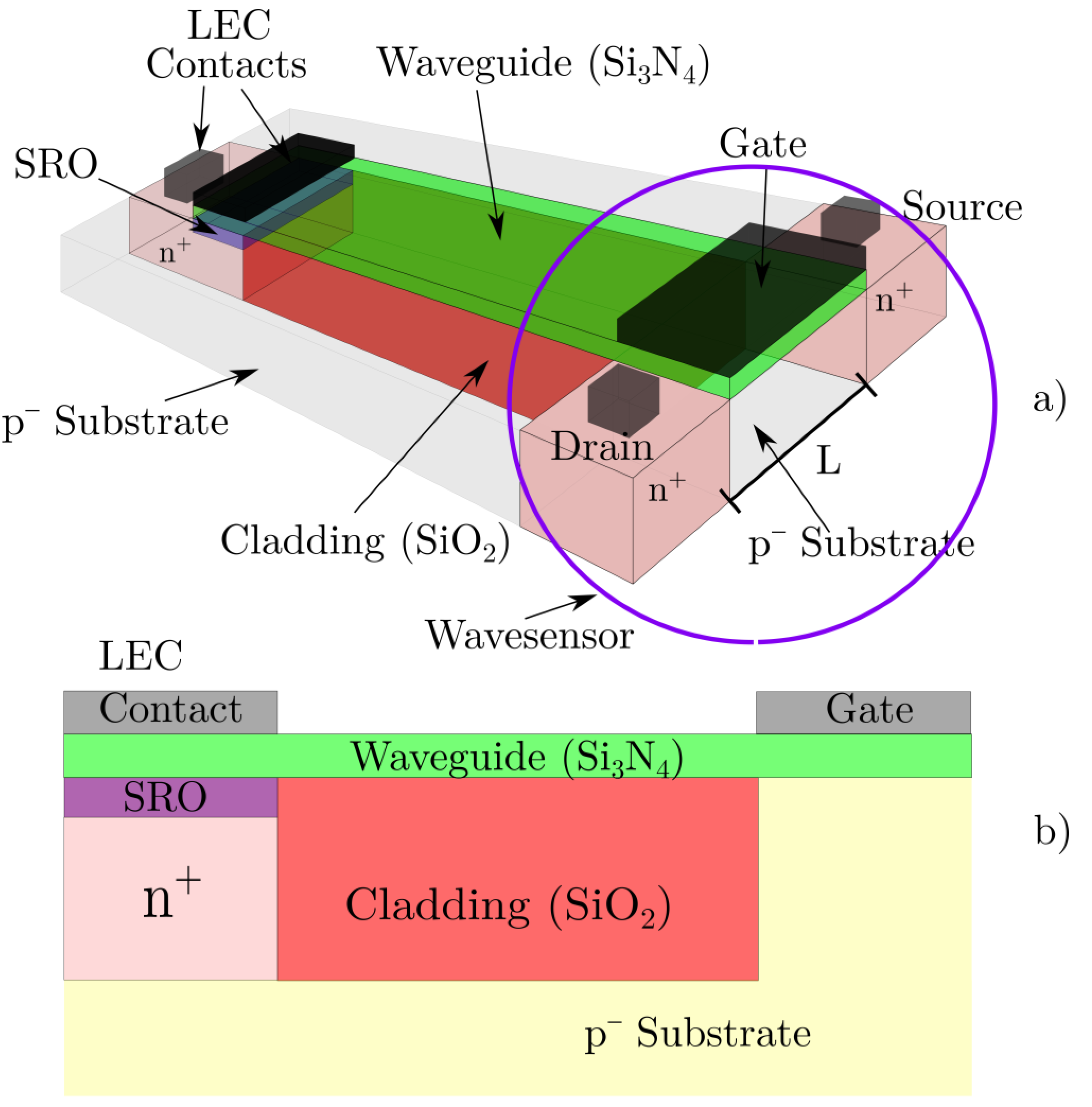
A descriptive schematic of the proposed integrated circuit is presented in Figure 1. This shows the LEC, the waveguide, and the photodetector. As can be seen, the wavesensor is a MIS-like structure, with the insulator being simultaneously an integrated silicon nitride (Si3N4) planar waveguide core, extended into below the gate contact metal.
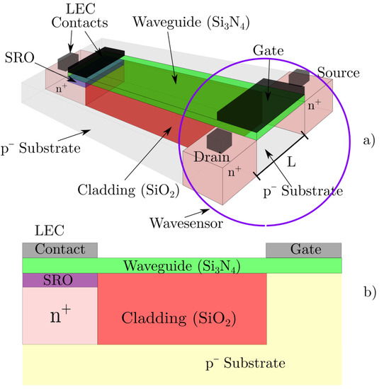
Figure 1.
Representation of the integrated circuit with the waveguide from the LEC up to the MIS-like WS (a). 2D schematic of the wavesensor, that is a MIS-like photodetector with the waveguide core being monolithically integrated under the gate terminal (b).
In the scheme of Figure 1, the light is produced by an SRO LEC and injected into the silicon nitride waveguide core. The waveguide ends on the WS, and the gate metal is on the top of the nitride core. With this configuration, the light is absorbed directly by the photodetecting region as follows: since the buried SiO2 lower cladding ends exactly at the edge of the WS, the radiation is transmitted with low losses until it reaches the gate area, and when the SiO2 cladding reaches the edge of the Si substrate part of the WS, the change in refractive index allows the transmission of the light from the waveguide to the silicon, right below the gate. The photons transfer energy to the WS to produce electron-hole pairs, which causes drain current variations. Note that this is not a regular photonic or electronic device, as no external light input-output ports exist, and the only way to inject light is through the waveguide core.
To estimate the viability of the concept and its detection characteristics, the phenomena taking place in the device were studied, in order to propose optimal fabrication parameters. Computational simulations were then carried out to confirm the viability and expected behavior of the WS.
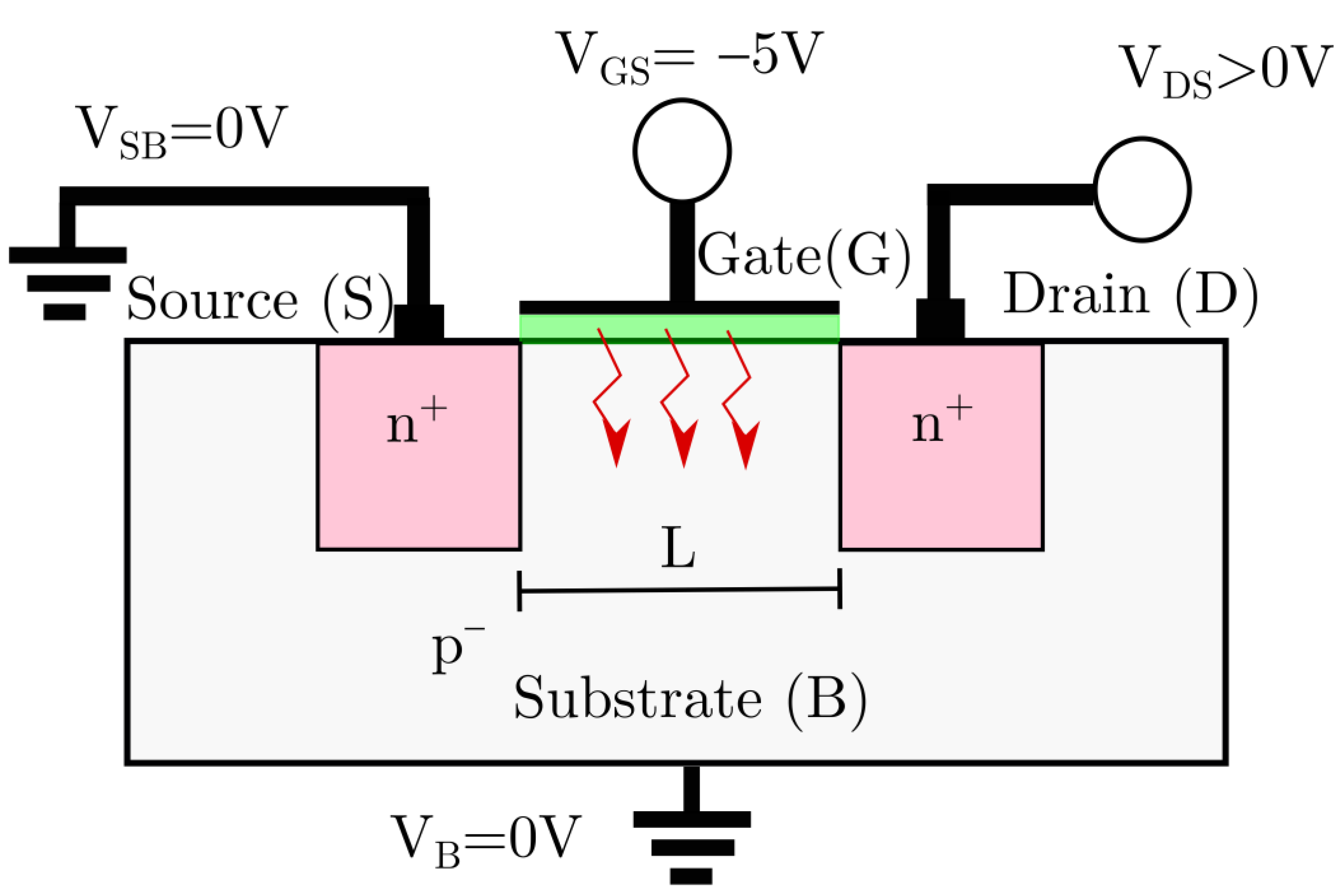
Following the process reported in [5], the substrate was a p-doped Silicon with acceptor concentration NA of 1 × 1014 cm−3. The distance between source and drain L, and the width of the transistor W, were, respectively, 5 μm and 1 μm. Drain and source regions were obtained through phosphor implantation prior to a thermal rediffusion at 1100 °C for 180 min. The nitride waveguide/gate insulator was obtained by chemical vapor deposition, and the thickness of the film was 140 nm. The metal used for the contacts was aluminum with thickness of 1 μm. After the fabrication, electrical and optical simulations were performed. Substrate and source contacts were biased to 0 V, and the gate voltage was −5 V. The drain voltage was varied from 0 V to 5 V. The light source was modeled using a uniform beam with wavelength (λ) of 600 nm and light power (Pin) varied from 0 nW to 50 nW, as reported for SRO-based light sources [12]. Figure 2 shows the 2D schematic of the WS.

Figure 2.
Schematic of the wavesensor (WS). The red arrows represent the lighting from the nitride waveguide directly into the depletion layer.
4. Electrical Behavior and Photodetection
4.1. Electrical Current
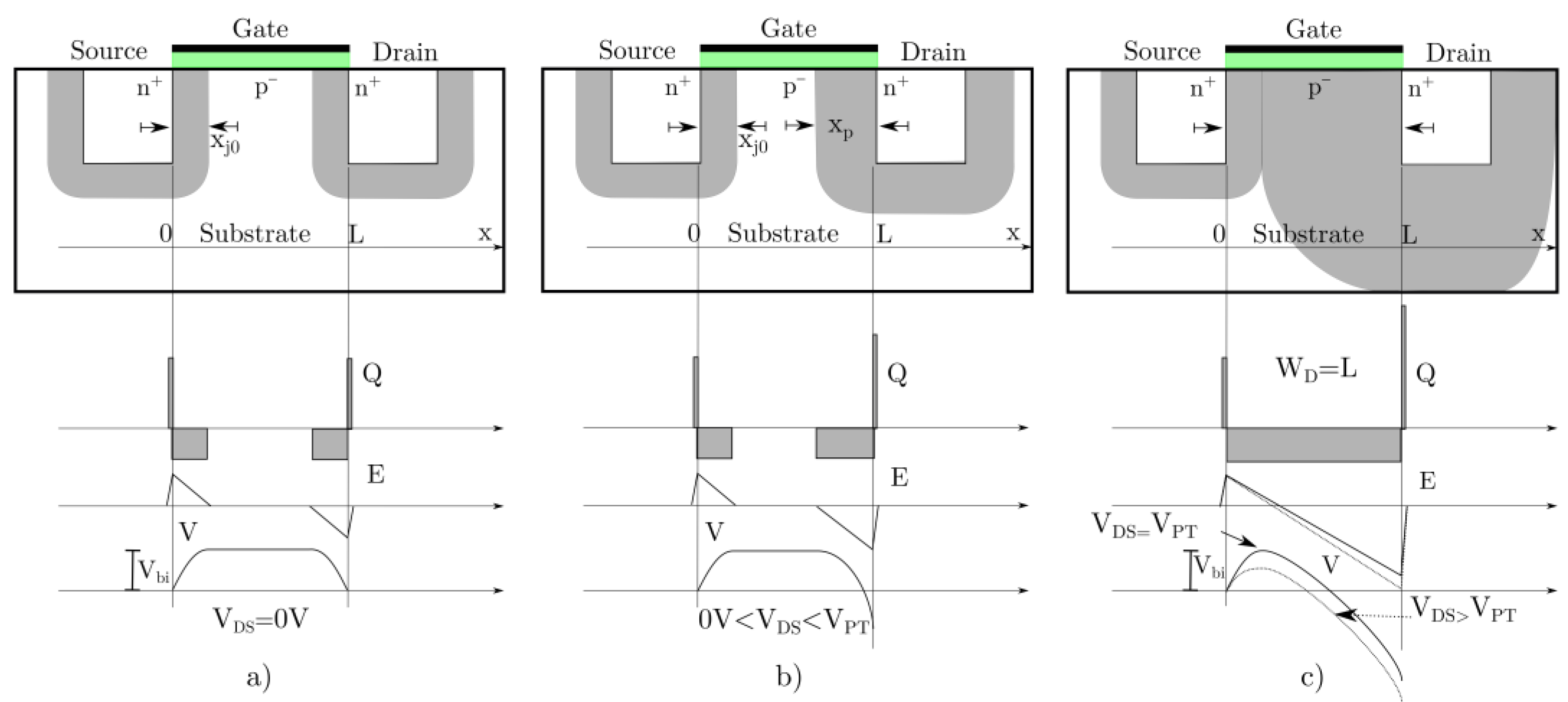
In Figure 3a, the applied voltages on the drain, source, and substrate are 0 V (VB = VS = VD = 0 V). The gate is biased in accumulation regime and its effect is just to avoid surface currents. The light is detected through the variation of the source to drain current produced by the absorption of the light directly into the depletion layer, below the extended waveguide core. The proposed device operates in Punch-Through regime. The lateral depletion zones of the source and drain overlap when the drain-source voltage VDS reaches the Punch-Through voltage VPT, as illustrated in Figure 3c. An electric current from source to drain is established under this bias condition. As an approximation, the analysis of the physics will be carried out in a substrate depth corresponding to the middle of source and drain. This reduces the analysis to two PN junctions separated by the depleted substrate below the gate area, as illustrated in Figure 3.
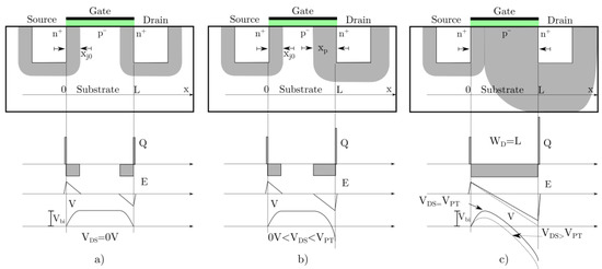
Figure 3.
Idealized scheme of the WS showing the charge, electric field and voltage profiles for the WS under thermal equilibrium (a), biased with VDS < VPT (b), biased with VDS ≥ VPT (Punch-Through) (c).
Figure 3a shows the charge (Q), electric field (E), and voltage (V) profiles obtained under equilibrium conditions using the depletion approximation [26,27,28]. Donor and acceptor profiles are assumed to be constant in the N and P zones. The p-n junctions (drain-substrate and source-substrate) are considered abrupt. Under these assumptions, the charges on the depleted zones are as show in Figure 3, and comply with charge neutrality condition (1):
where xn is the depletion width on the n-regions (drain and source) and xp the depletion width on the substrate region. As drain and source are heavily doped, the depletion width has a larger extension inside the substrate. The junctions produce a built-in voltage Vbi, as shown in Figure 3a. Since the electric charge is constant in the depletion zone, the electric field presents a linear profile with a maximum in the metallurgical junction. Calculating the integral of the electric field, a parabolic voltage profile can be obtained.
Figure 3b shows the profiles when drain is biased. When drain-substrate junction is reversely biased, the depletion width is increased. The depletion width under reverse bias can be calculated using (2) [27,29]:
When VDS = 0 V, the depletion width has an initial value called xj0, also showed in Figure 3. As VDS increases, the depletion regions grow wider, to the point where Punch-Through is reached at VDS = VPT. That is, both depletion regions overlap. The Punch-Through voltage (VPT) can be calculated using (3).
Figure 3c shows the profiles when VDS > VPT and Punch-Through is assured. The substrate region under the gate is fully depleted. If VDS continues increasing beyond VPT, the electric field increases enough to act on the source-substrate junction. The drain voltage induces a reduction of the potential barrier between source and substrate, as depicted in the bottom of Figure 3c. This can be interpreted as an induced forward voltage on this junction. The barrier reduction and the high drain voltage promotes a current flow towards the drain on Punch-Through regime. The current density in the depletion region jSCR is space charge limited, and has been proposed as a main current mechanism in devices working in this regime, as expressed in (4) [30,31,32,33,34]:
where εS is the silicon permittivity, μ is the electron mobility, and L is the distance between the source and drain. The current jSCR has a quadratic dependence on the drain voltage. As the device is kept in the Punch-Through regime, variation of VPT will produce variation in the jSCR.
An additional current arises as a result of the effect of drain voltage (VDS) on the source. This is represented as an equivalent forward voltage, VF(VDS). For low injection from the source to the depleted region at low electric fields, this current can be expressed as (5) [35,36,37,38]:
where Dn is the diffusion constant for electrons, LD is the Debye Length, k The Boltzmann Constant, T the temperature, ni the intrinsic concentration, and VF is the induced forward voltage caused by the drain voltage, which triggers a potential barrier reduction. Additional carrier generation in the substrate, such as optical or thermal, could also modify the effective VF, affecting jn. This perturbation stimulates an excess of current, which can be reflected in the total drain current.
It is also expected an influence of the gate voltage on the substrate surface, affecting its conductivity. However, these phenomena are to be addressed in a future work. For the present study, it was assumed a gate bias point corresponding to flat band or accumulation, making the superficial drain-source current negligible.
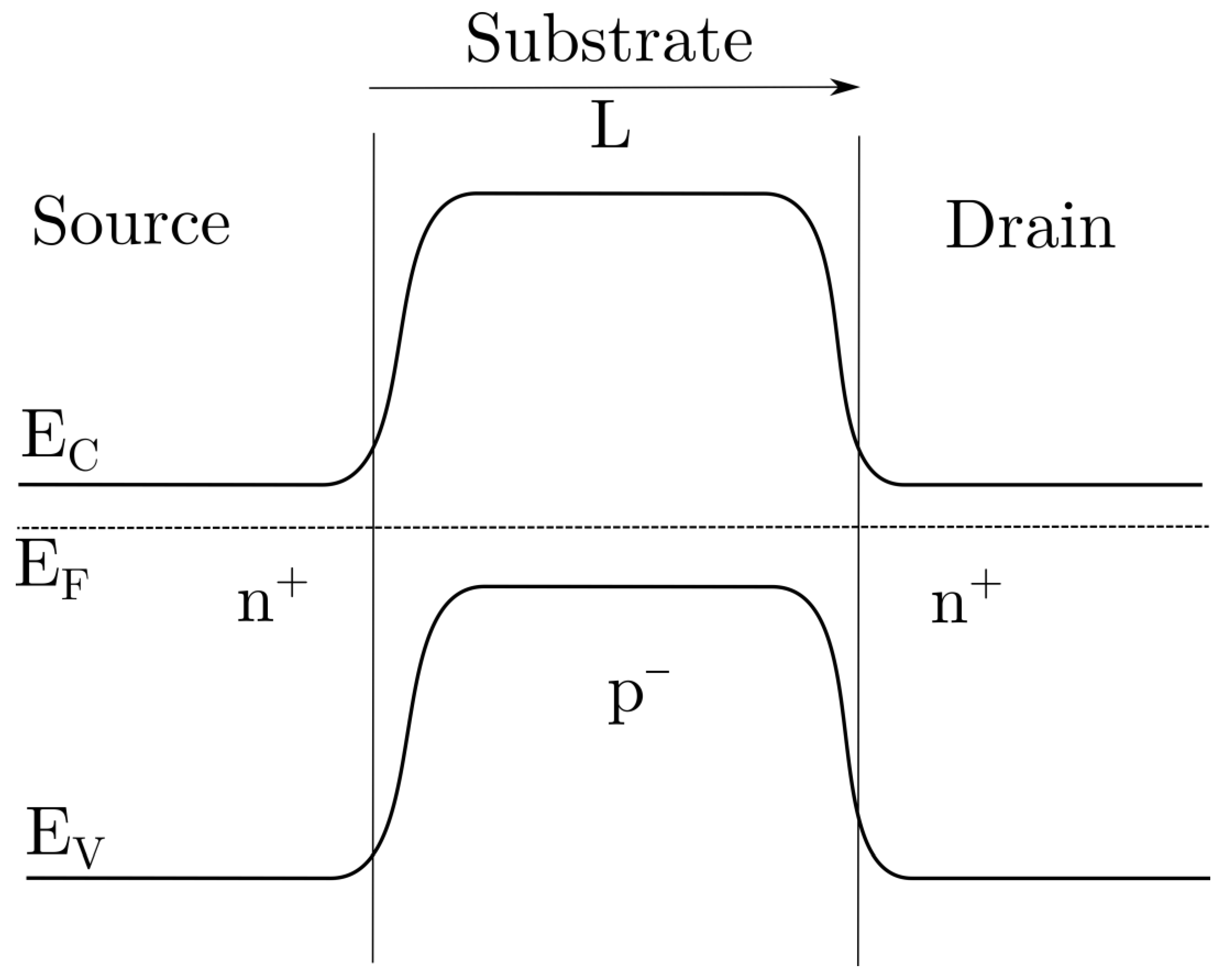
4.2. Energy Band Behavior on Dark Condition
Figure 4 illustrates the energy levels of the conduction band (EC), valence band (EV) and the Fermi level (EF) along source, bulk and drain for a WS with p-type substrate. The evaluation is at a middle depth in the n+ wells, where surface effects are negligible.

Figure 4.
Energy band diagrams at thermal equilibrium for a WS.
At this initial condition, drain current is not established due to the potential barriers. When the WS is biased with VDS > 0 V, band bending is produced and probability of carrier injection is increased. The drain voltage produces a drain-substrate junction reverse biased, increasing the width of depletion. As the drain voltage increments, the depleted zone in the drain increases, until both drain and source depletion regions overlap. This is known as Punch-Through condition, at VDS = VPT. The value of VPT is proportional to the separation L between source and drain. At Punch-Through, the voltage barrier reduces, as shown in Figure 5. Then, an electric current can be established due to the higher carrier injection probability.
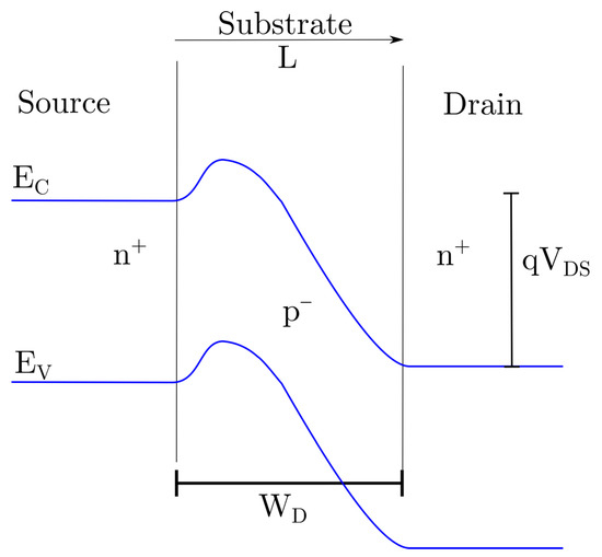
Figure 5.
Energy band diagrams for a WS on Punch-Through condition.
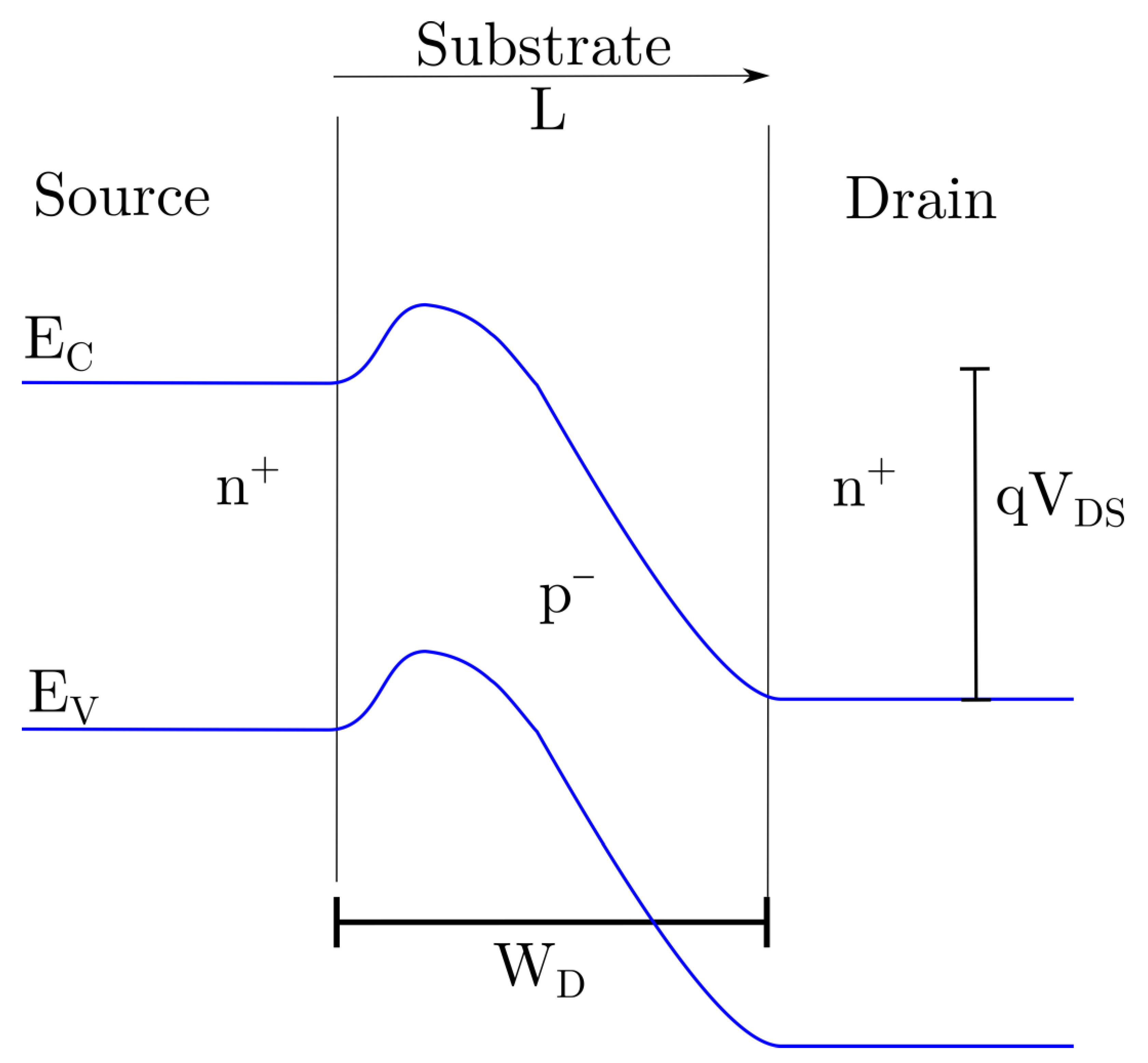
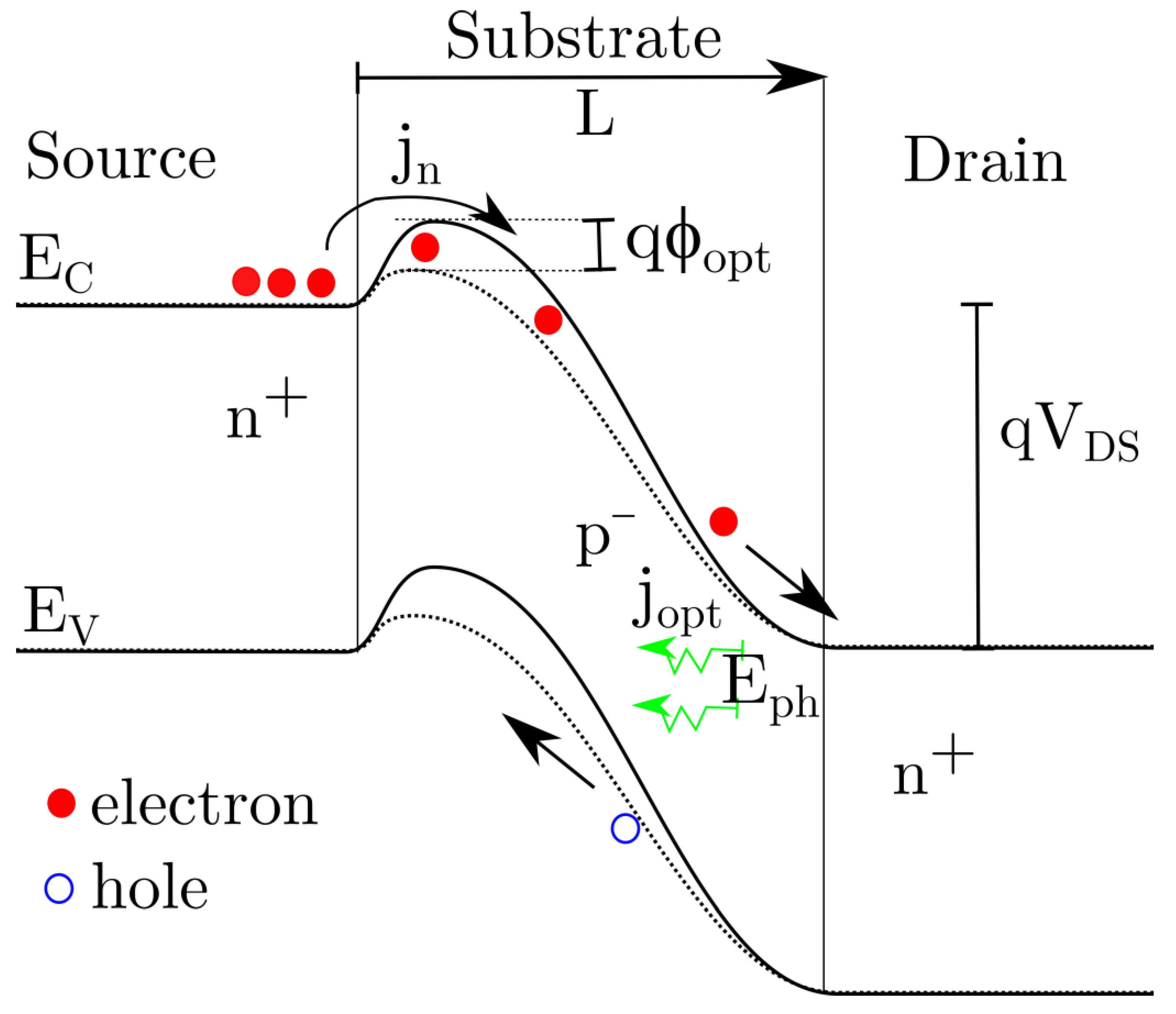
4.3. Energy Bands under Illumination Condition
If the drain-source junction is biased beyond Punch-Through condition, and light with an optical power Pin is absorbed by the silicon below the gate area, electron-hole pairs are produced in the space charge region between drain and source. This mechanism is depicted in Figure 6.
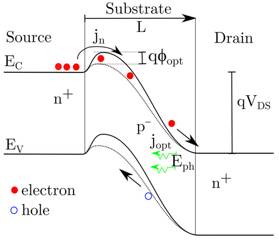
Figure 6.
Energy diagram for WS on Punch-Through under stimulation of light with absorbed photons with energy Eph. Red dots represent the electrons and blue dots the holes.
Absorbed photons with energy Eph greater than the band gap Eg produce electron-hole pairs, the electric field inside the depletion region separates the pair, and a current Iph is established. If it is assumed that each absorbed photon generates one electron-hole pair, then the current corresponding to photons Iph under ideal conditions can be calculated with (6).
where h, is the Planck constant, c the speed of light in vacuum, λ the wavelength, and Pin the incident optical power. This is the maximum current that can be generated by the absorbed light in a photodiode or any photodetector. However, the transduction of light in silicon present losses due to recombination processes, and only a portion of the generated electron-hole pairs end up contributing to the detectable current Iopt, which always is lower than Iph, depending on the quantum efficiency η as indicated in (7):
In addition, a Fermi quasi-level variation is produced by the optical carrier excess, and then the potential barrier is additionally reduced, promoting the injection of extra carriers from source to drain. Then, a current of electrons from the source jn is added to the photogenerated current. Assuming the WS is biased at low voltage, and a low injection regime, jn current is expressed as (8):
Here, VFeff is known as the effective induced source voltage, and is composed by a potential VF induced by the drain-source bias, plus the optical potential induced by photogenerated carrier excess ϕopt.
The total electron drain current density jdtotal can be expressed as (10):
Using (7), we can obtain jopt, which is the photocurrent density generated in the substrate within the space charge region. This current can be simplified into (11):
where A, is the cross-section area of the space charge region. In the presented configuration of the device, an optical current of holes is established through the substrate junction. This can be computed using (12) [39,40]:
Using this current, and considering that hole and electron currents are of the same magnitude, it is possible to estimate the optical potential as:
Combining (9), (10) and (13), the total equivalent drain current density can be expressed as:
in which the second and third terms account for to the presence of light. If the dark current is subtracted, the optical contribution to current jdopt can be identified:
Remember jopt represents the photocurrent density, taking into account quantum efficiency. Then, the ratio of jdopt to jopt delivers a value which, in case of being larger than 1, indicates an optical gain. This is β expressed in (16):
This is the gain of the WS.
4.4. General Summary of the Principles of Operation
The WS integrates a light emitter, waveguide, and a photodetector. In spite that it is a MOS-like structure, its operation is significantly different from the usual electrical amplification mechanisms. First, the proposed sensor is a bulk device, not a surface one. The metal gate has the only purpose of controlling the surface to avoid superficial current flow. The waveguide is also the dielectric under gate, making these devices electrophotonic and not electronic nor photonic. The device works in Punch-Through condition, extending as much as possible the sensing region length, increasing the photon conversion. In addition, the light is directly absorbed in the depleted region, without passing through highly doped or non-fully transparent materials. In Punch-Through condition, the high electric field moves the carriers towards the drain terminal. Drain current consists of two components: one produced by the carriers generated by light, and another made by electrons injected from Source. In the presence of light, the latter is increased due to a reduction of the barrier in the source-substrate interface, adding extra carriers to those directly photogenerated. This results in a gain on the photocurrent.
5. Results
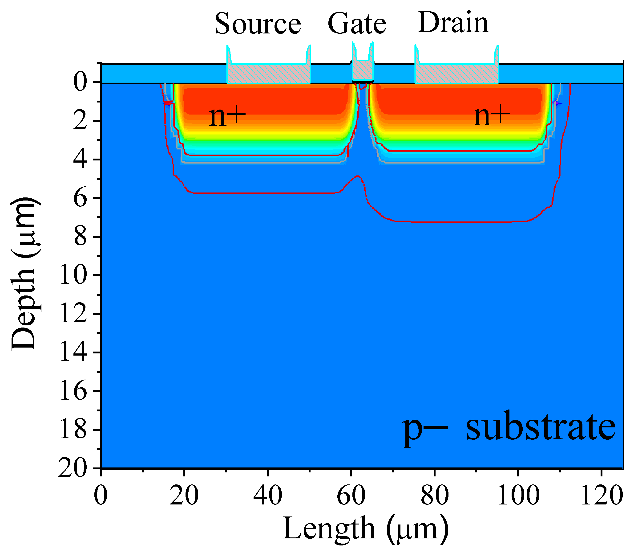
Figure 7 depicts a cross-section of the device in the Punch-Through regime as obtained by fabrication process simulation using SILVACO-Athena.
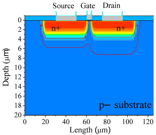
Figure 7.
WS obtained in Athena-Silvaco. Red lines show the edge of the depletion width when the drain is biased on Punch-Through.
The drain and source diffusions are heavily doped and have a depth junction of around 4 μm. This is due to the thermal treatment necessary in SRO-based light emitters, which is 1100 °C for 180 min [5]. As mentioned, the fabrication process was simulated using these thermal treatment conditions because the device is intended to work with an embedded SRO emitter, for full and monolithic integration.
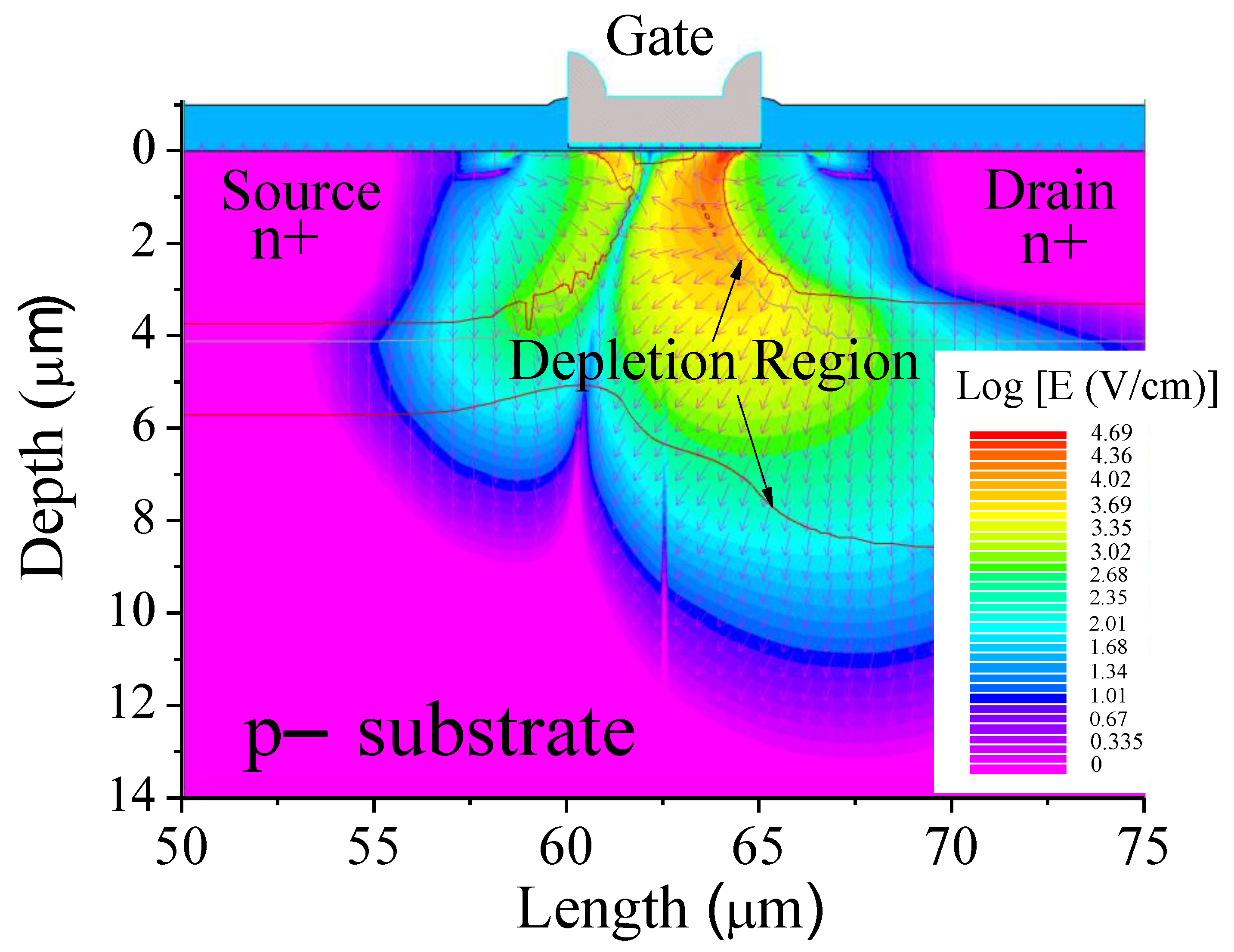
To simulate its photoelectric behavior, the gate was biased at VGS = −5 V, in order to promote hole accumulation in the surface. This way, the drain current can be exclusively controlled by the drain-source voltage, and current effects due to surface phenomena are avoided. The drain-source voltage applied was VDS = 5 V, causing the overlap of the depletion zones around drain and source (Punch-Through condition). For the wavelengths of interest, the absorption depth in silicon is located inside the depletion region, approximately from 0.1 μm to 10 μm for respective wavelength limits of 400 nm and 800 nm [27,41]. Figure 8 shows the electric field profile for the WS under the mentioned bias conditions.

Figure 8.
Electric Field inside the simulated WS. The direction is showed with arrows and the magnitude is represented in logarithmic scale with color levels. VDS was 5 V, VBS was 0 V and VGS was −5 V.
The strongest electric field is located close to the drain zone, caused by the VDS voltage. If electron-hole pairs are produced in the space charge region, the electric field transports the electrons into the drain terminal, and the holes are separated towards the substrate. Note the accumulated region in the surface, indicating no surface current can go through. Figure 9 shows the drain current as a function of drain voltage, considering both dark and light stimulation conditions.
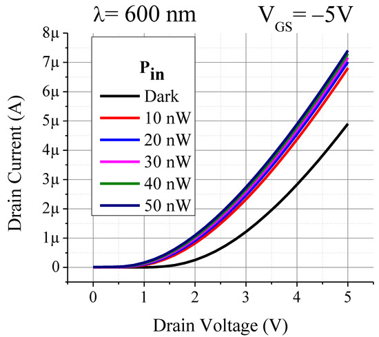
Figure 9.
Drain current as function of drain voltage under illumination for different optical powers.
As mentioned, a negative value of VGS prevents carrier transport through the surface, and the current is dominated by carrier generated in the substrate. The drain current-voltage behavior under this condition fits a quadratic curve. This is consistent to the mechanism of space charge limited current. If drain current in dark condition IDdark is subtracted from the total observed current when there is light ID, it can be obtained the contribution of light to the drain current IDopt. If the ratio of this value to the ideal photocurrent (Iph) is larger than one, it can be concluded that the device exhibits an optical gain βopt, as predicted by the previous analysis. This is presented in (17):
Figure 10 shows such photocurrent ratios for different optical powers and drain voltage.
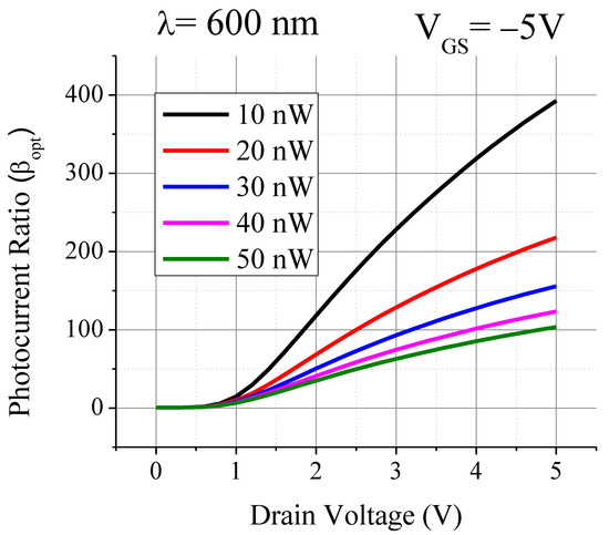
Figure 10.
Photocurrent ratio, βopt for different optical power as a function of drain voltage.
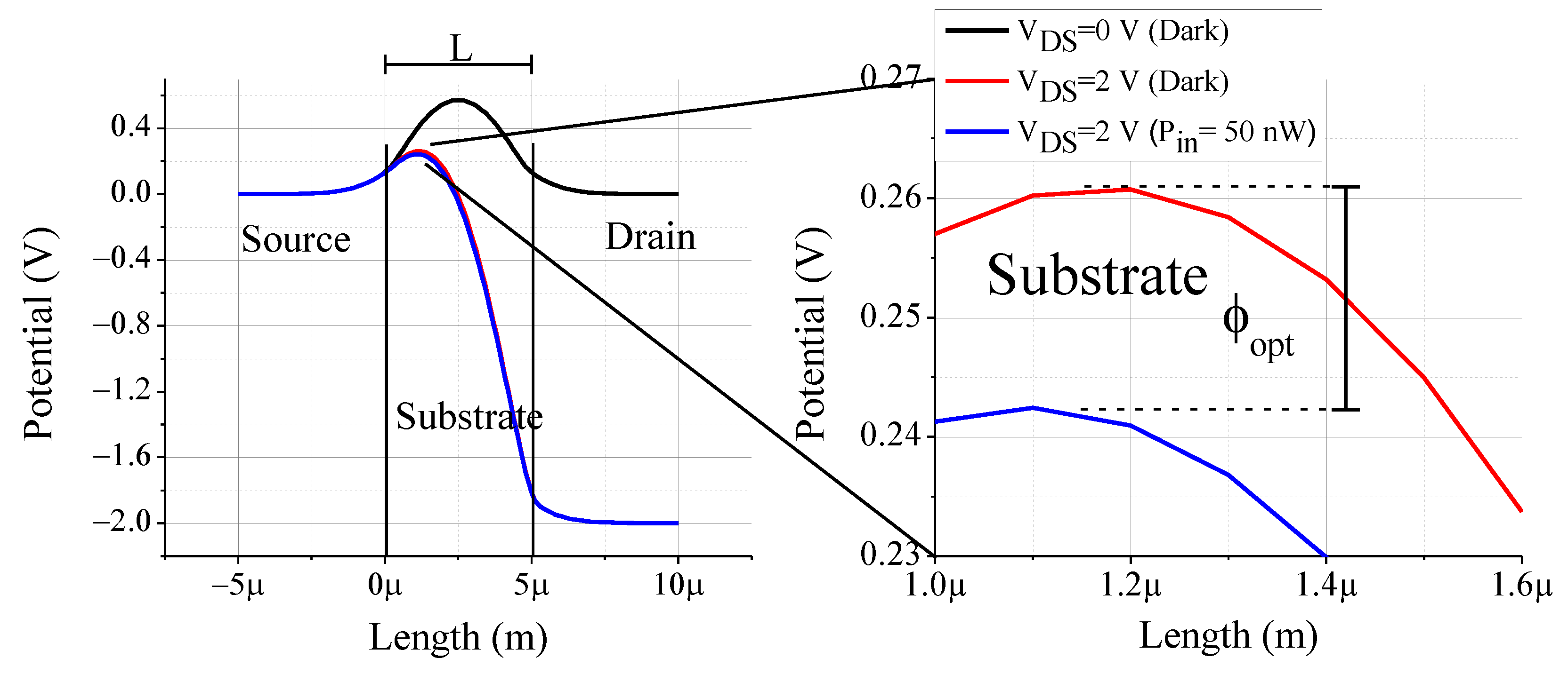
βopt is approximately 100 for VDS = 2 V when light power is 10 nW. It reaches 400 when VDS = 5 V. Note that, although the gain increases with the drain voltage, the dark current is also incremented. Then, there is a compromise between photocurrent gain and keeping the dark current low. It can be seen that the obtained gain is reduced when the optical power is increased. In spite more research is needed to better understand this phenomenon, this can be related to the variation of the Fermi quasi-level produced by the photo generated carrier excess. That is, the higher the input light power, the more influential the effect of photogeneration on the source barrier. The variation of the potential height as obtained by the simulations can be observed in the Figure 11.

Figure 11.
Potential profile for different drain bias and light stimulation. Light produces a reduction of the potential height in the source-substrate edge. The caption shows a zoom view of the specified range.
When voltage is applied to the drain, the drain-substrate junction is reversely biased, causing a reduction of potential height in the source-substrate junction as compared to equilibrium position. Incident optical power produces further potential reduction, promoting an additional injection of electrons from the source to the drain, thus obtaining a flow of carriers larger than the produced by electron-hole generation only, given place to the gain current in the WS. This indicates that the observed electro-optical gain phenomenon is due to a light-induced reduction of the potential barrier in the drain-substrate junction, as predicted from the analysis presented in the previous section.
6. Conclusions
In this paper, we propose a new electrophotonic sensor named wavesensor, conceived to be integrated with a silicon light source and a waveguide. The physics and mathematics involved in its operation have been developed, and a technological process parameters were suggested. The compatibility of the device with CMOS standard process has been demonstrated through computational simulation. It was mathematically demonstrated that light in the visible range is detected in the bulk and not in the surface, so the WS is a bulk device. The surface should be in accumulation regime to avoid parasitic currents. Light in the visible range, with powers in the order of nanowatts produces a photocurrent that is amplified by the WS. The silicon nitride waveguide core assures direct coupling with both the low optical power light source and the WS, in such a way that photons are injected directly to the depleted region without passing through a highly doped region. The photocurrent gain has a dependence on drain voltage. Computational simulations corroborated the mathematical model developed.
Author Contributions
Conceptualization, J.H.-B., A.A.G.-F. and M.A.-M.; methodology, J.H.-B., A.A.G.-F. and M.A.-M.; formal analysis, J.H.-B.; investigation, J.H.-B. and M.A.-M.; data curation, A.A.G.-F.; writing—original draft preparation, J.H.-B. and A.A.G.-F.; writing—review and editing, A.A.G.-F. and M.A.-M.; visualization, J.H.-B.; supervision, A.A.G.-F. and M.A.-M. All authors have read and agreed to the published version of the manuscript.
Funding
This project has received funding from the European Union’s Horizon 2020 research and innovation program under the Marie Skłodowska-Curie grant agreement No 801342 (Tecniospring INDUSTRY).
Institutional Review Board Statement
Not applicable.
Informed Consent Statement
Not applicable.
Data Availability Statement
The simulation data that support the findings of this study are available in INAOE institutional repository [42].
Acknowledgments
The authors acknowledge the support from CONACyT of Mexico.
Conflicts of Interest
The authors declare no conflict of interest.
References
- Kim, G.; Park, H.; Joo, J.; Jang, K.S.; Kwack, M.J.; Kim, S.; Kim, I.G.; Oh, J.H.; Kim, S.A.; Park, J.; et al. Single-Chip Photonic Transceiver Based on Bulk-Silicon, as a Chip-Level Photonic I/O Platform for Optical Interconnects. Sci. Rep. 2015, 5, 11329. [Google Scholar] [CrossRef] [PubMed] [Green Version]
- Chen, X.; Milosevic, M.M.; Stanković, S.; Reynolds, S.; Bucio, T.D.; Li, K.; Thomson, D.J.; Gardes, F.; Reed, G.T. The Emergence of Silicon Photonics as a Flexible Technology Platform. Proc. IEEE 2018, 106, 2101–2116. [Google Scholar] [CrossRef] [Green Version]
- Sun, H.; Xu, K.; Zhao, J.; Zhang, J.; Zhou, Y.; Liu, L.; Yuan, J.; Huang, L.; Zhu, K.; Snyman, L.W.; et al. A Dependency of Emission Efficiency of Poly-Silicon Light-Emitting Device on Avalanching Current. Opt. Mater. 2019, 88, 711–717. [Google Scholar] [CrossRef]
- Misiakos, K.; Makarona, E.; Hoekman, M.; Fyrogenis, R.; Tukkiniemi, K.; Jobst, G.; Petrou, P.S.; Kakabakos, S.E.; Salapatas, A.; Goustouridis, D.; et al. All-Silicon Spectrally Resolved Interferometric Circuit for Multiplexed Diagnostics: A Monolithic Lab-on-a-Chip Integrating All Active and Passive Components. ACS Photonics 2019, 6, 1694–1705. [Google Scholar] [CrossRef]
- González-Fernández, A.A.; Juvert, J.; Aceves-Mijares, M.; Domínguez, C. Monolithic Integration of a Silicon-Based Photonic Transceiver in a CMOS Process. IEEE Photonics J. 2016, 8, 7900213. [Google Scholar] [CrossRef]
- Fernández, A.A.G.; Sánchez, A.M.; Leyva, K.M.; Mijares, M.A. A MOS-like Electroluminescent Device Based on Silicon-Rich Oxide. In Proceedings of the 2009 6th International Conference on Electrical Engineering, Computing Science and Automatic Control (CCE), Toluca, Mexico, 10–13 January 2009. [Google Scholar] [CrossRef]
- Cabañas-Tay, S.A.; Palacios-Huerta, L.; Aceves-Mijares, M.; Alvarez-Quintana, J.; Pérez-García, S.A.; Domínguez-Horna, C.; Morales-Sánchez, A. Influence of the Gate and Dielectric Thickness on the Electro-Optical Performance of SRO-Based LECs: Resistive Switching, IR and Deep UV Emission. J. Lumin. 2017, 192, 919–924. [Google Scholar] [CrossRef]
- Huang, B.; Zhang, X.; Dong, Z.; Wang, W.; Chen, H. Monolithic Integration of Light Emitting Diodes, Photodetector and Receiver Circuit in Standard CMOS Technology. In Proceedings of the 2008 9th International Conference on Solid-State and Integrated-Circuit Technology, Beijing, China, 20–23 October 2008; pp. 985–987. [Google Scholar] [CrossRef]
- Wang, Z.; Abbasi, A.; Dave, U.; De Groote, A.; Kumari, S.; Kunert, B.; Merckling, C.; Pantouvaki, M.; Shi, Y.; Tian, B.; et al. Novel Light Source Integration Approaches for Silicon Photonics. Laser Photonics Rev. 2017, 11, 1700063. [Google Scholar] [CrossRef]
- Pavesi, L. Silicon-Based Light Sources for Silicon Integrated Circuits. Adv. Opt. Technol. 2008, 2008, 416926. [Google Scholar] [CrossRef] [Green Version]
- Juvert, J.; Gonzalez Fernandez, A.A.; Morales-Sánchez, A.; Barreto, J.; Aceves, M.; Llobera, A.; Dominguez, C. DC Electroluminescence Efficiency of Silicon Rich Silicon Oxide Light Emitting Capacitors. J. Light. Technol. 2013, 31, 2913–2918. [Google Scholar] [CrossRef]
- González-Fernández, A.A.; Juvert, J.; Aceves-Mijares, M.; Domínguez, C. Luminescence from Si-Implanted SiO2-Si3N4 Nano Bi-Layers for Electrophotonic Integrated Si Light Sources. Sensors 2019, 19, 865. [Google Scholar] [CrossRef] [PubMed] [Green Version]
- Palacios-Huerta, L.; Cabañas-Tay, S.A.; Luna-López, J.A.; Aceves-Mijares, M.; Coyopol, A.; Morales-Sánchez, A. Effect of the Structure on Luminescent Characteristics of SRO-Based Light Emitting Capacitors. Nanotechnology 2015, 26, 395202. [Google Scholar] [CrossRef] [PubMed]
- Alarcón-Salazar, J.; Palacios-Huerta, L.; González-Fernández, A.A.; Morales-Sánchez, A.; Aceves-Mijares, M. Monolithically Integrable Si-Compatible Light Sources. In Recent Development in Optoelectronic Devices; Srivastava, R., Ed.; IntechOpen: Rijeka, Croatia, 2018. [Google Scholar] [CrossRef]
- Aceves-Mijares, M.; González-Fernández, A.A.; López-Estopier, R.; Luna-López, A.; Berman-Mendoza, D.; Morales, A.; Falcony, C.; Domnguez, C.; Murphy-Arteaga, R. On the Origin of Light Emission in Silicon Rich Oxide Obtained by Low-Pressure Chemical Vapor Deposition. J. Nanomater. 2012, 2012, 890701. [Google Scholar] [CrossRef]
- Piels, M.; Bowers, J.E. Photodetectors for Silicon Photonic Integrated Circuits; Elsevier Ltd.: Amsterdam, The Netherlands, 2016. [Google Scholar] [CrossRef]
- Sun, C.; Wade, M.T.; Lee, Y.; Orcutt, J.S.; Alloatti, L.; Georgas, M.S.; Waterman, A.S.; Shainline, J.M.; Avizienis, R.R.; Lin, S.; et al. Single-Chip Microprocessor That Communicates Directly Using Light. Nature 2015, 528, 534–538. [Google Scholar] [CrossRef] [PubMed] [Green Version]
- Li, H.; Zhang, S.; Zhang, Z.; Zuo, S.; Zhang, S.; Sun, Y.; Zhao, D.; Zhang, Z. Silicon Waveguide Integrated with Germanium Photodetector for a Photonic-Integrated Fbg Interrogator. Nanomaterials 2020, 10, 1683. [Google Scholar] [CrossRef] [PubMed]
- Alarcón-Salazar, J.; Vázquez, G.V.; González-Fernández, A.A.; Zaldívar-Huerta, I.E.; Pedraza-Chávez, J.; Aceves-Mijares, M. Waveguide-Detector System on Silicon for Sensor Application. Adv. Mater. Lett. 2018, 9, 116–122. [Google Scholar] [CrossRef]
- Muñoz, P.; Micó, G.; Bru, L.A.; Pastor, D.; Pérez, D.; Doménech, J.D.; Fernández, J.; Baños, R.; Gargallo, B.; Alemany, R.; et al. Silicon Nitride Photonic Integration Platforms for Visible, near-Infrared and Mid-Infrared Applications. Sensors 2017, 17, 2088. [Google Scholar] [CrossRef]
- Blumenthal, D.J.; Heideman, R.; Geuzebroek, D.; Leinse, A.; Roeloffzen, C. Silicon Nitride in Silicon Photonics. Proc. IEEE 2018, 106, 2209–2231. [Google Scholar] [CrossRef] [Green Version]
- Roeloffzen, C.G.H.; Hoekman, M.; Klein, E.J.; Wevers, L.S.; Timens, R.B.; Marchenko, D.; Geskus, D.; Dekker, R.; Alippi, A.; Grootjans, R.; et al. Low-Loss Si3N4 Triplex Optical Waveguides: Technology and Applications Overview. IEEE J. Sel. Top. Quantum Electron. 2018, 24, 4400321. [Google Scholar] [CrossRef] [Green Version]
- Porcel, M.A.G.; Hinojosa, A.; Jans, H.; Stassen, A.; Goyvaerts, J.; Geuzebroek, D.; Geiselmann, M.; Dominguez, C.; Artundo, I. Silicon Nitride Photonic Integration for Visible Light Applications. Opt. Laser Technol. 2019, 112, 299–306. [Google Scholar] [CrossRef]
- González-Fernández, A.A.; Hernández-Montero, W.W.; Hernández-Betanzos, J.; Domínguez, C.; Aceves-Mijares, M. Refractive Index Sensing Using a Si-Based Light Source Embedded in a Fully Integrated Monolithic Transceiver. AIP Adv. 2019, 9, 125215. [Google Scholar] [CrossRef] [Green Version]
- Alarcón-Salazar, J.; Vásquez-Agustín, M.A.; Quiroga-González, E.; Zaldívar-Huerta, I.E.; Aceves-Mijares, M. Comparison of Light Emitting Capacitors with Textured and Polished Silicon Substrates towards the Understanding of the Emission Mechanisms. J. Lumin. 2018, 203, 646–654. [Google Scholar] [CrossRef]
- Shockley, W. The Theory of P-n Junctions in Semiconductors and p-n Junction Transistors. Bell Syst. Tech. J. 1949, 28, 435–489. [Google Scholar] [CrossRef]
- Sze, S.M. Semiconductor Devices. Physics and Technology, 3rd ed.; John Wiley & Sons: Hoboken, NJ, USA, 2012. [Google Scholar] [CrossRef]
- Grove, A.S.; Fitzgerald, D.J. Surface Effects on P-n Junctions: Characteristics of Surface Space-Charge Regions under Non-Equilibrium Conditions. Solid State Electron. 1966, 9, 783–806. [Google Scholar] [CrossRef]
- Grove, A.S. Physics and Technology of Semiconductor Devices; Wiley International Edition; Wiley: Hoboken, NJ, USA, 1967. [Google Scholar]
- Denda, S.; Nicolet, M.A. Pure Space-Charge-Limited Electron Current in Silicon. J. Appl. Phys. 1966, 37, 2412–2424. [Google Scholar] [CrossRef] [Green Version]
- Büget, U.; Wright, G.T. Space-Charge-Limited Current in Silicon. Solid State Electron. 1967, 10, 199–207. [Google Scholar] [CrossRef]
- Richman, P. Modulation of Space-Charge-Limited Current Flow in Insulated-Gate Field-Effect Tetrodes. IEEE Trans. Electron Devices 1969, 16, 759–766. [Google Scholar] [CrossRef]
- Wilamowski, B.M.; Jaeger, R.C.; Fordemwalt, J.N. Buried-Channel MOS Transistor with Punch-Through. Solid State Electron. 1984, 27, 811–815. [Google Scholar] [CrossRef]
- Wilamowski, B.M.; Jaeger, R.C. The Lateral Punch-through Transistor. IEEE Electron Device Lett. 1982, 3, 277–280. [Google Scholar] [CrossRef]
- Lohstroh, J.; Koomen, J.J.M.; Van Zanten, A.T.; Salters, R.H.W. Punch-through Currents in P+NP+ and N+PN+ Sandwich Structures-I. Introduction and Basic Calculations. Solid State Electron. 1981, 24, 805–814. [Google Scholar] [CrossRef]
- Lohstroh, J.; Koomen, J.J.M.; Van Zanten, A.T.; Salters, R.H.W. Punch-through Currents in P+NP+ and N+PN+ Sandwich Structures—II. Solid State Electron. 1981, 24, 815–820. [Google Scholar] [CrossRef]
- Esener, S.; Lee, S.H. Punch-through Current under Diffusion-Limited Injection: Analysis and Applications. J. Appl. Phys. 1985, 58, 1380–1387. [Google Scholar] [CrossRef]
- Płotka, P.; Wilamowski, B. Interpretation of Exponential Type Drain Characteristics of the Static Induction Transistor. Solid State Electron. 1980, 23, 693–694. [Google Scholar] [CrossRef]
- Sah, C.T. The Spatial Variation of the Quasi-Fermi Potentials in p-n Junctions. IEEE Trans. Electron Devices 1966, ED-13, 839–846. [Google Scholar] [CrossRef]
- Roenker, K.P.; Primel, S.M.; Cahay, M.M. Effects of Optical Absorption on the Quasi-Fermi Level Splitting at the Emitter-Base Junction in Npn Heterojunction Bipolar Phototransistors. IEEE Trans. Electron Devices 1999, 46, 669–674. [Google Scholar] [CrossRef]
- Green, M. Self-Consistent Optical Parameters of Intrinsic Silicon at 300 K Including Temperature Coefficients. Sol. Energy Mater. Sol. Cells 2008, 92, 1305–1310. [Google Scholar] [CrossRef]
- Aceves-Mijares, M. Simulation Data Electrophotonic Waveguide Transistor Photodetector; INAOE: Puebla, Mexico, 2020. [Google Scholar]


Publisher’s Note: MDPI stays neutral with regard to jurisdictional claims in published maps and institutional affiliations. |
© 2022 by the authors. Licensee MDPI, Basel, Switzerland. This article is an open access article distributed under the terms and conditions of the Creative Commons Attribution (CC BY) license (https://creativecommons.org/licenses/by/4.0/).