Article

The Dependence of InAs/InAsSb Superlattice Detectors’ Spectral Response on Molecular Beam Epitaxy Growth Temperature

by
Krystian Michalczewski
1,
Jarosław Jureńczyk
1,
Łukasz Kubiszyn
1 and
Piotr Martyniuk
2,3,*
1
VIGO System S.A., 129/133 Poznańska St., 05-850 Ożarów Mazowiecki, Poland
2
Institute of Applied Physics, Military University of Technology, 2 Kaliskiego St., 00-908 Warsaw, Poland
3
Department of Electrical Engineering, The Ohio State University, 2024 Neil Avenue, Columbus, OH 43210, USA
*
Author to whom correspondence should be addressed.
Appl. Sci. 2022, 12(3), 1368; https://doi.org/10.3390/app12031368
Submission received: 11 December 2021 / Revised: 17 January 2022 / Accepted: 20 January 2022 / Published: 27 January 2022
(This article belongs to the Section Materials Science and Engineering)

Abstract

:
In this paper, we report on the influence of molecular beam epitaxial (MBE) growth temperature on the spectral response of the long-wavelength infrared radiation (LWIR), three-stage thermoelectrically (TE) cooled (T = 210, 230 K) InAs/InAsSb type-II superlattice (T2SL)-based detectors grown on the GaSb/GaAs buffer layers/substrates. Likewise, antimony (Sb) composition and the superlattice (SL) period could be used for spectral response selection. The presented results indicate that the growth temperature affects the 50% cut-off (λ50%cut-off) of the fabricated devices and could be used for operating wavelength tunning. Assuming constant Sb composition and T2SL period during MBE process, the growth temperature is presented to influence λ50%cut-off covering entire LWIR (e.g., temperature growth change within the range of 400–450 °C contributes to the λ50%cut-off ~ 11.6–8.3 μm estimated for operating temperature, T = 230 K). An increase in temperature growth makes a blueshift of the λ50%cut-off, and this is postulated to be a consequence of a modification of the SL interfaces. These results show an approach to the T2SL InAs/InAsSb deposition optimization by the growth temperature in terms of the spectral response, without influencing the T2SLs’ structural properties (Sb composition, SL period).

1. Introduction

Long-wavelength infrared radiation (LWIR; 8–12 µm) is still one of the most exploited spectral ranges for military, spectroscopy, gas sensing, or meteorology applications [1,2]. Nowadays, due to the improvement of epitaxial techniques, especially molecular beam epitaxy (MBE), the superlattice (SL) concept presented by Esaki and Tsu in 1970 has presented itself as a potential candidate (proved by many scientific papers) to supersede HgCdTe [3]. SL detectors made of III-V materials have stronger covalent bonds than HgCdTe, which results in a higher operating temperature range and better material uniformity [4]. Growth temperature is one of the most important control parameters during the MBE process. Omitting the problem connected with the temperature measurements inside the chamber, it is commonly known that the growth temperature (Tgrowth) mainly influences crystal quality. Over the past few years, the dependence of the crystal quality, nucleation mode, and carrier mobility on the Tgrowth of the simple bulk semiconductor structures has been investigated, to find the optimal growth condition. However, research data are lacking for much more sophisticated structures such as type-II superlattice (T2SLs) [5,6,7]. The T2SL InAs/InAsSb is a quantum structure consisting of connected InAs and InAsSb layers (generally with an antimony (Sb) composition, xSb ~ 0.4). The structure is designed to be lattice matched to GaSb substrate or GaSb buffer layer/GaAs substrate. The ideal T2SL InAs/InAsSb structure consists of sharp interfaces without the addition of any extra sublayers such as in T2SLs InAs/GaSb, as shown in Figure 1 [8].
In the real T2SL, it is hard to obtain defect-free interfaces, especially when a thin InAsSb layer is utilized. This requires growth interruptions and necessitates soaking time between each layer. Moreover, the potential composition changes at the interfaces are hard to predict. These interface issues are directly responsible for discrepancies between a theoretical computer simulation of band structure and experimental results. In this study, we show that the MBE growth temperature can indirectly affect the detector’s spectral response, just as a thicker SL period or higher Sb composition results in a redshift of λ50%cut-off InAs/InAsSb T2SLs, which gives flexibility in detector’s designing procedure without influencing any SL structural parameters. In this paper, a series of T2SL InAs/InAsSb detectors optimized for the LWIR range were investigated with a particular focus on the growth temperature, in order to show the cut-off wavelength range tunning for LWIR.

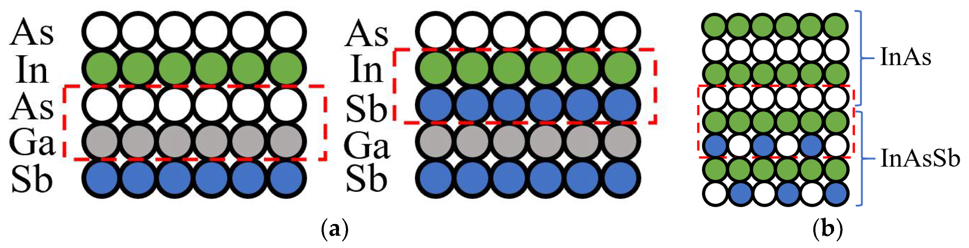
2. Material Growth Procedure

Each T2SL InAs/InAsSb structure was grown in a RIBER Compact 21-DZ solid source MBE system, on 2” semi-insulating GaA (001) substrates. The substrate temperature during the growth was monitored by a manipulator thermocouple. The substrate temperature was the only parameter being changed intentionally during the growth campaigns. A detailed description of the buffer layer growth and substrate preparation procedure can be found elsewhere [9]. The T2SLs growth conditions and parameters were adapted after Lee et al. and Sarney et al. [10,11]. The GaA substrates were used to implement low-cost substrates in the mass fabrication of the backside-illuminated devices. Two sets of samples were prepared. The T2SL growth parameters are presented in Table 1. The approx. 300 periods (P) T2SLs InAs/InAsSb were grown on 250 nm GaAs smoothing layer, followed by 1.2 µm thick GaSb buffer on the GaAs substrates. The 1.2 µm thick buffer connected with interfacial misfit array (IMF) growth mode allowed high-quality structures to be obtained without any surface corrugations for the IR photoconductor’s final fabrication [12,13,14].
Sets I and II differ in the superlattice period and include samples with and without beryllium (Be) doping marked, respectively (superscripts: “+”; “−”), as shown in Table 1. The Be doping was used to increase the final device sheet resistance, and it is not a focus of this research. The Be doping is used to reach the HOT condition for the LWIR detectors—that is why Be–p-type doping was implemented. Auger generation recombination rates are strongly dependent on temperature via the dependence of carrier concentration and intrinsic times on temperature. Therefore, cooling is one of the effective ways to suppress Auger processes. Since intrinsic τA7 is larger than intrinsic τA1, Auger processes can be minimized also by optimized p-type doping. An optimized p-type significantly improves the performance, compared with that of an undoped material, but excessive doping lowers the device’s performance [15].
High-resolution X-ray diffraction (PANalytical X’Pert—HRXRD) was utilized to assess the structural properties of the T2SLs InAs/InAsSb. The MBE growth temperature is presented as a variation from a nominal value ~425 °C. This is motivated by the general problem of the temperature representation in the MBE chamber. There are three dominant methods of temperature measurements: pyrometer, thermocouple of the manipulator (used here), or the BadniT system. Each method exhibits its own limitation, and the combination of at least two was used in the early stage for the growth condition optimization. The value ~425 °C represents optimal growth parameters in our MBE chamber, which included the type of manipulator, substrate, and molybdenum block thicknesses or molecular beams.
Figure 2 presents the HRXRD spectra for the samples given in Table 1. The full-width at half-maximum (FWHM) values of the 0th/GaSb-order HRXRD peaks of the analyzed T2SL samples should be considered indicators of the grown T2SLs material quality and are presented in Table 1.
The samples were optimized in terms of the material used during the MBE growth procedure and lattice-matched condition to GaSb buffer, which was confirmed by ∆a/a GaAs-0th/GaSb, assuming 7.274% (average) for Set I and 7.273% for Set II samples, respectively. For Set I samples, the material quality improved as the substrate temperature decreased from 450 °C to 400 °C, and the lowest FWHMs were observed for the samples grown at 400 °C. For SET II, this behavior was not observed, and the highest FWHM corresponded to the longest λ50%cut-off (18 μm and 16 μm) and highest values of ∆a/a GaAs-0th/GaSb (7.312% and 7.278%). That is related to the non-intentional period and Sb composition distribution, which was also confirmed by the T2SLs’ high-order peak shift.
Samples were grown in different periods of time (all within three months of one another), with proper reproducibility. The 66.05° (in average) peak represents GaAs substrate, as presented in Figure 2a–d.
It must be stressed that the FWHM of the ~5 μm GaSb buffer layer grown on GaAs substrate changed from 120 arcsec to 130 arcsec, respectively. In our case, with the 1.2 μm GaSb buffer, the FWHM of the GaSb layer grown on GaAs substrate read ~200 arcsec [13]. It must be underlined that even if the intensity of T2SL InAs/InAsSb was much higher than from GaSb, the FWHM of the 0th peak was dominated by the GaSb buffer layer.
T2SLs InAs/InAsSb period and Sb composition values were simulated by PANalytical software, and their data are presented in Table 1. For the simulation, sharp interfaces between InAs/InAsSb were assumed.
In addition, the magnified 0th/GaSb HRXRD spectra for samples 4, 5, 6 (FWHM 236, 200, 180 arcsec) are presented in Figure 3. It must be stressed that an average (for samples 4, 5, 6) ∆a/a GaAs-0th/GaSb was 7.271%.

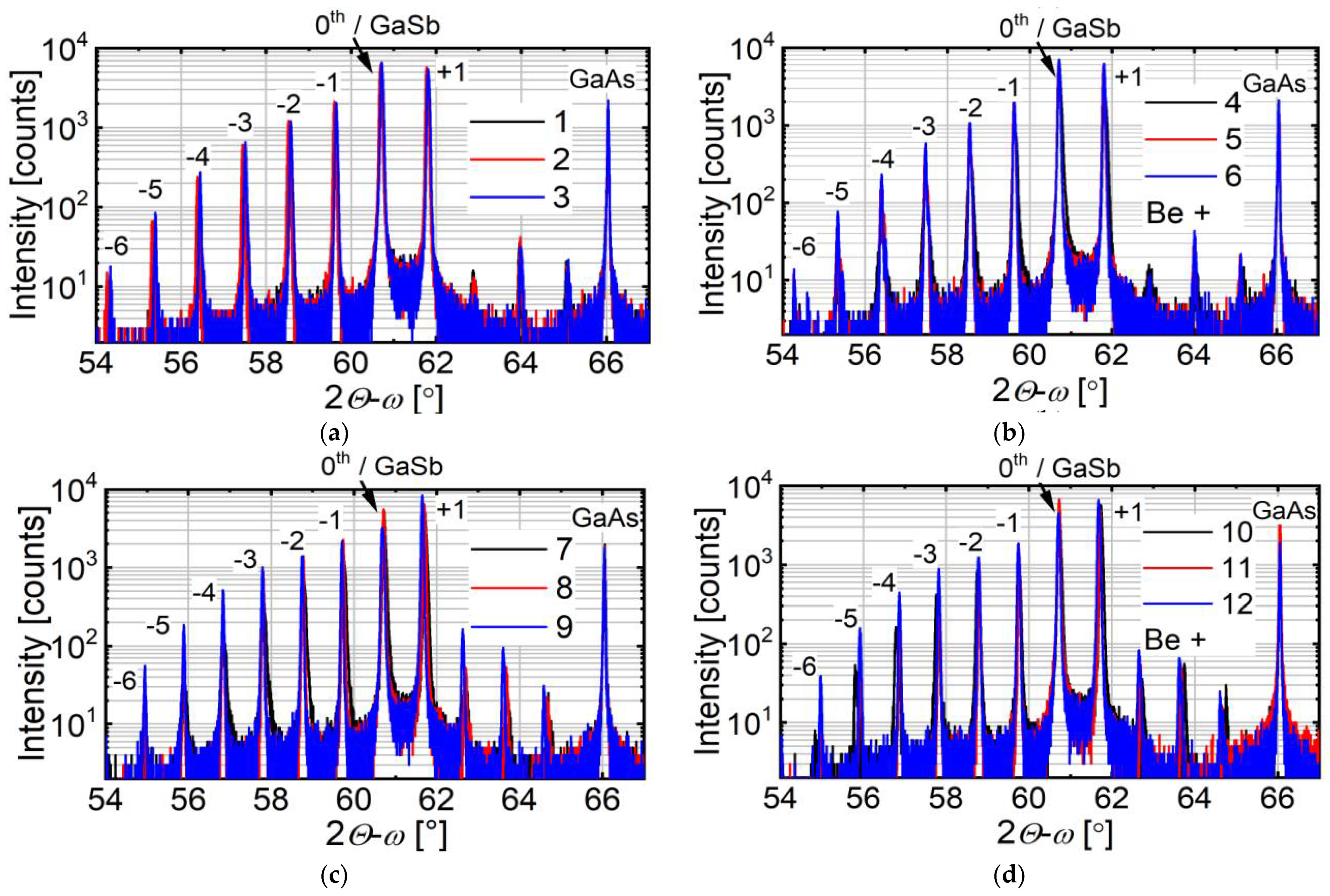
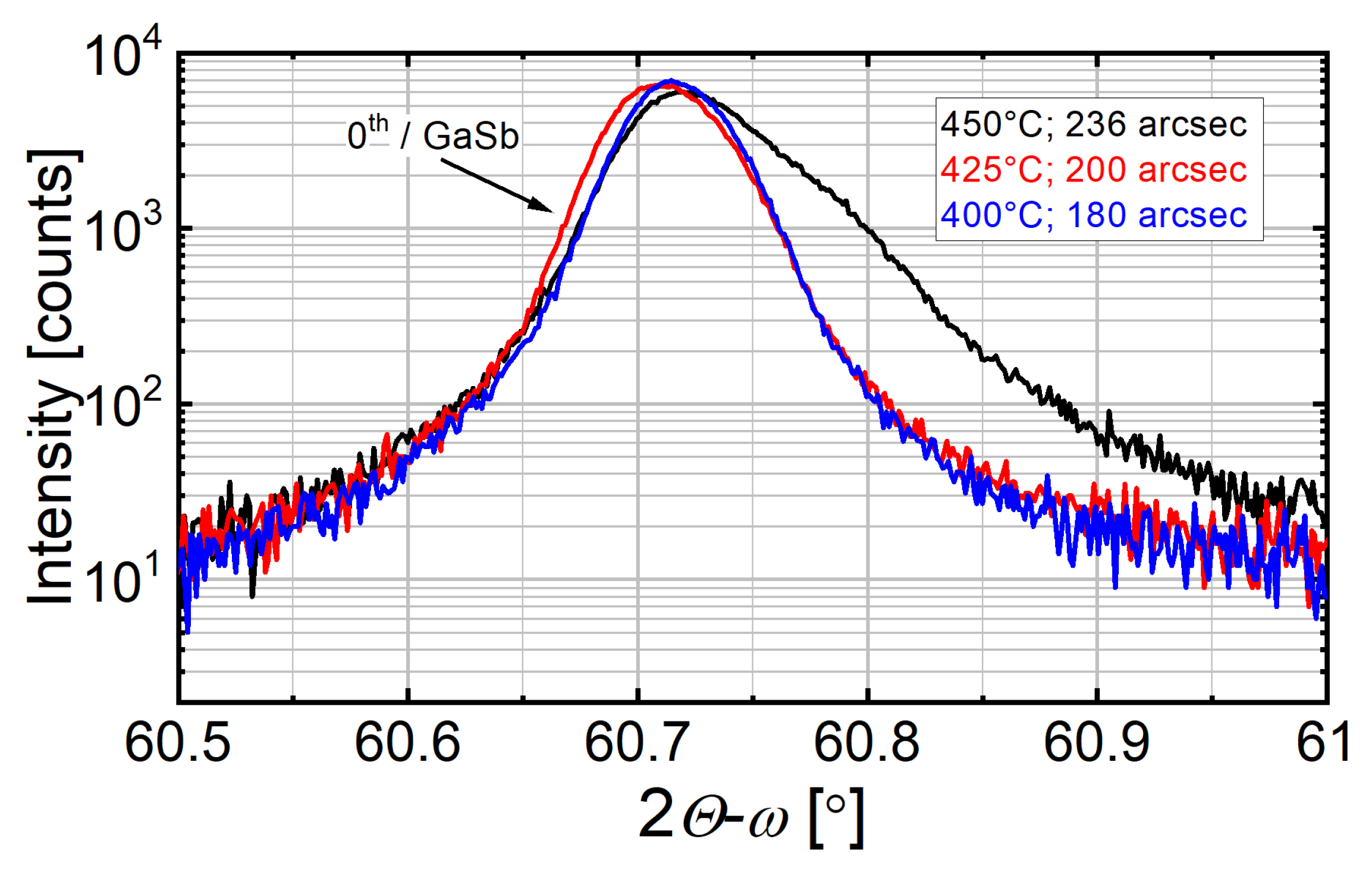
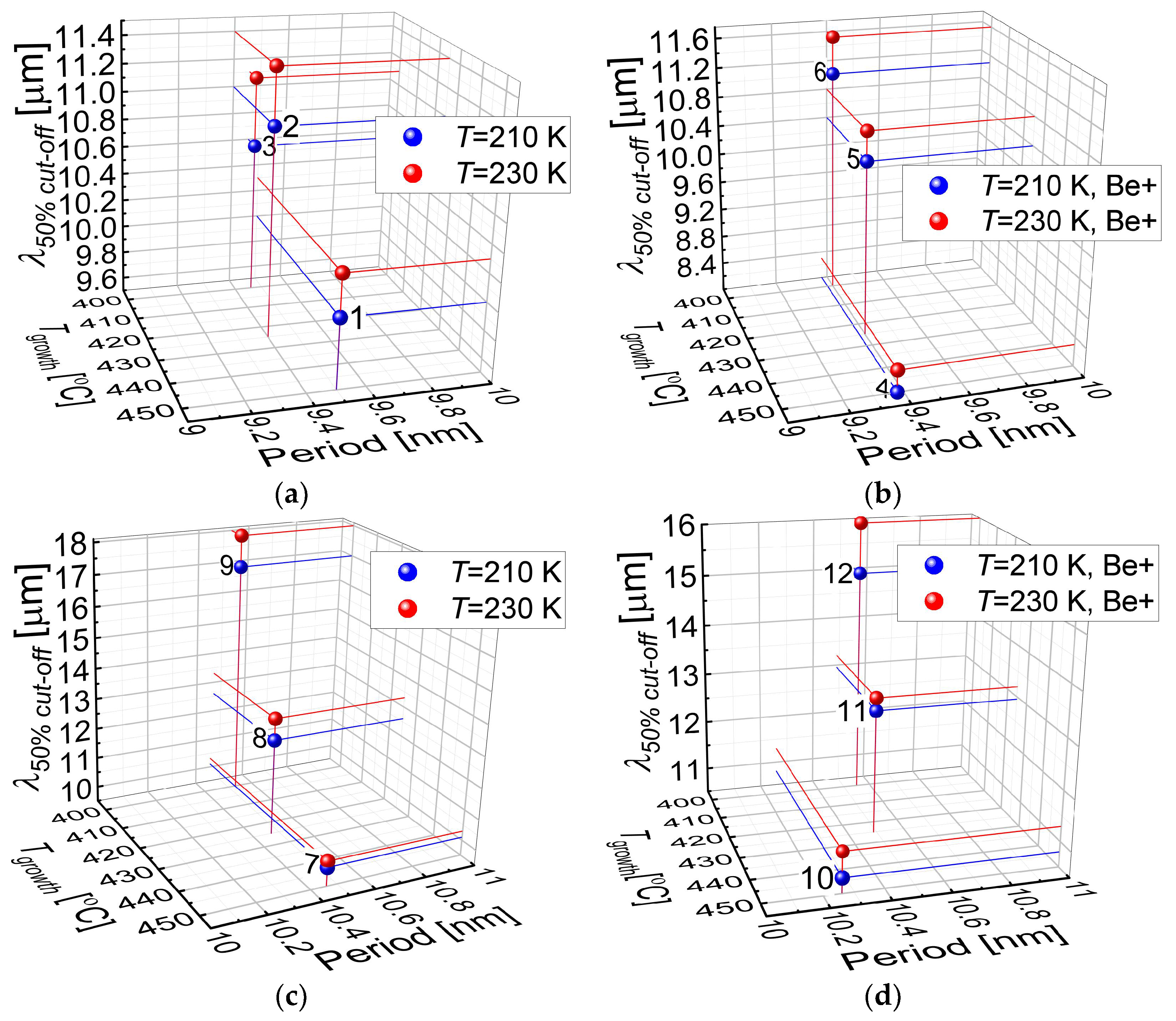
3. Optical Characterization

The photoconductors structures of the grown T2SLs InAs/InAsSb were processed with standard photolithography technique and wet etching. The intent T2SLs active layer thickness (l) was assumed at the level of 3 μm (Table 1). For Set 1, the number of periods (intentional number) was assumed at the level of 317. For Set 2 (intentional number), the number of periods was assumed at the level of 288. Period (P) and Sb composition were estimated based on XRD simulation. As presented in Table 1, thickness l varies within the range of 2.95–3.04 μm.
The spectral characteristics were presented by normalized responsivities (Rin) according to the following relation: R i n = R i ·   l E = λ η q h c τ μ e , where η is the quantum efficiency, q is the electron charge, l is the length between contacts, E is the electric field, and µe is the electron mobility. Rin enables the determination of responsivity (Ri) normalized versus electric field and device length. The spectrophotometer’s incident beam (which was used in experiments) illuminated all active areas of the photoconductor with the same incident power density. That minimized the device’s geometry contribution to the Rin.
Figure 4 and Figure 5 show the spectral characteristic versus temperature and wavelength (λ), respectively. λ50%cut-off correlated strongly versus growth temperature, with a marked redshift at 400 °C and blueshift at 450 °C. In addition to the blueshift, Set I samples grown at 450 °C showed broadening due to higher-order satellite peaks. Only Set I samples 1, 2, and 3 (Figure 4a) did not follow the trend in terms of the λ50%cut-off versus Tgrowth.
Investigation of the observed behavior was more complicated. The T2SLs InAs/InAsSb energy bandgap (Eg) is defined as a distance between valence and conduction minibands. The main factors contributing to the location of minibands are strain, InAsSb Sb composition (xSb), and T2SLs period (P) [16,17,18].
According to the measured structure properties, variations in the T2SLs period and Sb composition were small within each sample and assumed negligible in our analysis. The only interfaces regions within T2SLs InAs/InAsSb could affect the location of minibands. At the interfaces between InAs and InAsSb, the strain could be changed due to InAsSb Sb composition distribution within InAsSb and InAs layers, which will be discussed later.
Our research identified only two papers on the growth temperature influence on the T2SLs cut-off wavelength. Liu et al. changed the Tgrowth of T2SLs InAs/InAsSb from 400 °C to 450 °C. Unfortunately, the presented samples prepared for each temperature also differed in period and xSb, and no direct comparison was possible [19]. The Sb cross-incorporation into InAs layers was observed but also not explained.
The same situation could be found in a paper by Haugan et al. [20]. The samples were grown in selected temperatures without compensation of the As and Sb beams. The higher growth temperature lowers Sb composition in the InAsSb layer and changes the T2SL InAs/InAsSb bandgap. The detailed investigation of epitaxial T2SL InAs/InAsSb was carried out first by Wood et al. and later by Kim et al. [21,22]. In both papers, the authors measured interfaces of the same sample by scanning tunneling microscope (STM) and scanning transmission electron microscope (STEM), respectively. Wood et al. provided information on the interfaces inside the structure, where Sb segregation was observed and fitted to a standard segregation model formulated by Muraki et al. [23].
The newest results shown by Kotulak et al. indicate that the Sb in some circumstances (such as thin InAs layers) could be observed in all InAs regions, which contradicts the common As-to-Sb atom exchange at the interfaces [24]. The T2SLs presented by Kotulak et al. were fully Sb dispersed.
The preliminary theoretical calculations of Sb distribution in the InAsSb layer were presented by Lu et al. [25]. One of the important observations that could explain our results is that variation in Sb profiles results in blue- and redshifts and must be taken into consideration during bandgap engineering. Based on the observed changes in spectral characteristics, we believe that the distribution of Sb generally in InAsSb or even in the InAs layer can affect the strain, which could result in the observed bandgap variations, contributing to the cut-off wavelength changes assuming constant T2SLs Sb composition and period [24]. These results have been assessed theoretically in analyses presented by Lu et al. and Ciani et al. [25,26].
Given the necessity of soaking time at the InAs/InAsSb interfaces, the exchange reaction between As and Sb molecules on the surface is inevitable, and the assumption of abrupt interfaces in the T2SLs InAs/InAsSb theoretical simulations can lead to unrealistic results. Our results showed that Tgrowth is probably the main parameter influencing and modifying the Sb distribution at interfaces (or in all layers) in T2SLs InAs/InAsSb.

4. Discussion

As mentioned, the Sb distribution in InAsSb or even in the InAs layer can affect the strain, which could result in the observed energy bandgap changes versus Tgrowth. In order to present the Sb distribution in the InAsSb layer in the Set I samples 4, 5, and 6, Muraki’s model was incorporated [23]. In this model, the Sb background (xb) should be determined, and the R parameter corresponds to the rate of the As–Sb exchange in InAsSb. Knowing the T2SL period (P = 9.4 nm) and intended Sb profile (xSb = 0.39), one can simulate the Sb distribution profile (z-direction) according to the following relations:
  • x s b = x 0 ( 1 R z ) + x b for 0 < z < N;
  • x s b = x 0 ( 1 R N ) R z N + x b for N < z < P.
For the Set I samples 4, 5, and 6, we made the following assumptions related to Muraki’s model characteristic parameters versus growth temperature presented in Table 2.
The SIMS measurements show the Sb background composition at the level of ~5% [9]. The 3% Sb background, R = 0.7 (for the comparable growth temperature, Tgrowth = 420 °C) contributing to the similar Sb distribution in T2SLs InAs/InAsSb were reported by Kim et al. [22]. The InAsSb thickness (N) for which maximum Sb composition occurred was assumed at the level of 2 nm, assuming nominal InAsSb thickness 2.49 nm, similarly to the Sb composition distribution presented by Kim et al. [22].
When we increased the Tgrowth, the R parameter increased, which could result in higher Sb background composition (that is marked by arrows). Figure 6 presents the Sb composition distribution within the InAsSb layer (2.49 nm). We assumed the following R parameters for the Set I samples 4, 5, and 6: R = 0.9/0.7/0.4 and R = 0.8/0.7/0.6; these values correspond to the Tgrowth to present the 1D in-plane strain ( ε I I = ( a f a G a S b ) / a G a S b ) distribution within InAsSb (out-of-plane strain could be calculated by the equation ε = 2 C 12 / C 11 for (001) GaA substrates). The InAsSb layer was in compression in relation to the GaSb buffer layer for in-plane and in tensile for out-of-plane direction. It must be stressed that an average (for samples 4, 5, 6) ∆a/a GaAs-0th/GaSb was assumed as 7.271%. As presented in Figure 6a–d, a decrease in the exchange rate R parameter lowered Sb composition distribution and strain within the InAsSb layer in relation to GaSb. As mentioned above, the segregation efficiency R increases with growth temperature, as expected, the results of which are presented in Figure 6 [27].
The measured 100% cut-off wavelengths (λ100%cut-off) for Set I samples 4, 5, and 6 read ~9.4 μm (450 °C), ~11.5 μm (425 °C), and ~12.8 μm (400 °C) (Figure 7).
We calculated the energy bandgap dependence versus strain in T2SLs InAs/InAsSb (samples 4, 5, and 6) based on an 8 × 8 kp solver. The results are presented in Figure 8. Assuming average strain 1.27%, 0.6%, and 0.05% (Figure 6), our simulation results read the following measurements:
  • ~12.3 μm for 1.27%—(measured~12.8 μm);
  • ~10.9 μm for 0.6%—(measured~11.5 μm);
  • ~9.8 μm for 0.05%—(measured~9.4 μm).
The presented theoretical energy bandgap and λ100%cut-off trends versus Tgrowth followed the experimental results. The discrepancy is believed to be connected to the assumed abrupt interfaces in the T2SLs InAs/InAsSb. In addition, assuming strain-balanced conditions, the Sb composition drop increased the effective T2SLs InAs/InAsSb energy bandgap, which was also presented previously by Steenbergen et al. [28,29]. Our simulation results also followed the trend presented by Ting et al. for the T2SLs (3n, n) InAs/InAs0.6Sb0.4 [30]. According to the Sb composition distribution presented in Figure 6, the average Sb composition distribution decreases with an increase in the R parameter. In addition, it must be stressed that we made a theoretical assumption on strain distribution in the InAsSb layer (similar distribution was presented by Kim et al. [22]). In addition, it is revealed from data presented in Figure 6a–d that Sb distribution created extra strain in the InAs layer.

5. Conclusions

We presented observations of strain modification in T2SLs InAs/InAsSb introduced by Tgrowth within 400–450 °C (optimal 425 °C) and presented the results of changes in energy bandgap, contributing to the changes in spectral responses. The growth temperature is believed to impact the Sb distribution at the interfaces, and an increase in Tgrowth led to a blueshift of the λ50%cut-off. It was shown that the Tgrowth could be used to tune the operating wavelength in LWIR range (e.g., temperature growth change within the range 400–450 °C contributed to the λ50%cut-off ~ 11.6–8.3 μm, estimated for operating temperature T = 230 K), while keeping the period and Sb composition constant, which provides much more flexibility in the device’s design process without affecting T2SLs’ structural parameters—Sb composition and period.

Author Contributions

Conceptualization, P.M. and K.M.; methodology, K.M., Ł.K., J.J. and P.M.; validation, P.M. and K.M.; formal analysis, K.M. and P.M.; investigation, K.M., Ł.K. and J.J.; writing—original draft preparation, K.M. and P.M.; writing—review and editing, K.M. and P.M.; visualization, K.M. and P.M.; supervision, P.M.; project administration, P.M. All authors have read and agreed to the published version of the manuscript.

Funding

This research was funded by Polish National Science Center, grant numbers OPUS 2018/31/B/ST7/01541 and HARMONIA 2018/30/M/ST7/00174.

Data Availability Statement

The data that support the findings of this study are available from the corresponding author upon reasonable request.

Conflicts of Interest

The authors declare no conflict of interest.

References

  1. Leroy, C.; Chorier, P.; Destefanis, G. LWIR and VLWIR MCT technologies and detectors development at SOFRADIR for space applications. In Proceedings of the Infrared Technology and Applications XXXVIII, Baltimore, MA, USA, 23–27 April 2012; Volume 8353. [Google Scholar]
  2. Sagiv, L.; Rotman, S.R.; Blumberg, D.G. Detection and identification of effluent gases by long wave infrared (LWIR) hyperspectral images. In Proceedings of the 2008 IEEE 25th Convention of Electrical and Electronics Engineers, Eilat, Israel, 3–5 December 2008; pp. 413–417. [Google Scholar]
  3. Esaki, L.; Tsu, R. Superlattice and Negative Differential Conductivity in Semiconductors. IBM J. Res. Dev. 1970, 14, 61–65. [Google Scholar] [CrossRef]
  4. Bajaj, J.; Sullivan, G.; Lee, D.; Aifer, E.; Razeghi, M. Comparison of type-II superlattice and HgCdTe infrared detector technologies. In Proceedings of the Infrared Technology and Applications XXXIII, Orlando, FL, USA, 8 June 2007; Volume 6542, p. 65420B. [Google Scholar]
  5. Benyahia, D.; Kubiszyn, Ł.; Michalczewski, K.; Kębłowski, A.; Martyniuk, P.; Piotrowski, J.; Rogalski, A. Low-temperature growth of GaSb epilayers on GaAs (001) by molecular beam epitaxy. Opto-Electron. Rev. 2016, 24, 40–45. [Google Scholar] [CrossRef]
  6. Ayers, J.E. Heteroepitaxy of Semiconductors: Theory, Growth, and Characterization; CRC Press: Boca Raton, FL, USA, 2007. [Google Scholar]
  7. Kaiser, S.; Jakob, M.; Zweck, J.; Gebhardt, W.; Ambacher, O.; Dimitrov, R.; Schremer, A.T.; Smart, J.; Shealy, J.R. Structural properties of AlGaN/GaN heterostructures on Si(111) substrates suitable for high-electron mobility transistors. J. Vac. Sci. Technol. 2000, 18, 733–740. [Google Scholar] [CrossRef]
  8. Liu, Y.; Zhang, C.; Wang, X.; Wu, J.; Huang, L. Interface investigation of InAs/GaSb type II superlattice for long wavelength infrared photodetectors. Infrared Phys. Technol. 2011, 113, 103573. [Google Scholar] [CrossRef]
  9. Michalczewski, K.; Kubiszyn, Ł.; Martyniuk, P.; Wu, C.H.; Jureńczyk, J.; Grodecki, K.; Benyahia, D.; Rogalski, A.; Piotrowski, J. Demonstration of HOT LWIR T2SLs InAs/InAsSb photodetectors grown on GaAs substrate. Infrared Phys. Technol. 2018, 95, 222–226. [Google Scholar] [CrossRef]
  10. Lee, G.S.; Lo, Y.; Lin, Y.F.; Bedair, S.M.; Laidig, W.D. Growth of InAs1−xSbx (0<x<1) and InSb-InAsSb superlattices by molecular beam epitaxy. Appl. Phys. Lett. 1985, 47, 1219–1221. [Google Scholar] [CrossRef]
  11. Sarney, W.L.; Svensson, S.P. Flux dependent Sb-incorporation during molecular beam epitaxy of InAsSb. J. Vac. Sci. Technol. B 2015, 33, 060604. [Google Scholar] [CrossRef]
  12. Benyahia, D.; Kubiszyn, Ł.; Michalczewski, K.; Kębłowski, A.; Martyniuk, P.; Piotrowski, J.; Rogalski, A. Interfacial misfit array technique for GaSb growth on GaAs (001) substrate by molecular beam epitaxy. J. Electron. Mater. 2018, 47, 299–304. [Google Scholar] [CrossRef] [Green Version]
  13. Benyahia, D.; Kubiszyn, Ł.; Michalczewski, K.; Kębłowski, A.; Martyniuk, P.; Piotrowski, J.; Rogalski, A. Optimization of the interfacial misfit array growth mode of GaSb epilayers on GaAs substrate. J. Cryst. Growth 2018, 483, 26–30. [Google Scholar] [CrossRef]
  14. Benyahia, D.; Kubiszyn, Ł.; Michalczewski, K.; Kębłowski, A.; Martyniuk, P.; Piotrowski, J.; Rogalski, A. p-type doping of GaSb by beryllium grown on GaAs (001) substrate by molecular beam epitaxy. JSTS J. Semicond. Technol. Sci. 2016, 16, 695–701. [Google Scholar] [CrossRef] [Green Version]
  15. Piotrowski, J. Uncooled operation of IR photodetectors. Opto-Electron. Rev. 2004, 12, 111–122. [Google Scholar]
  16. Webster, P.T.; Riordan, N.A.; Liu, S.; Steenbergen, E.H.; Synowicki, R.A.; Zhang, Y.H.; Johnson, S.R. Measurement of InAsSb bandgap energy and InAs/InAsSb band edge positions using spectroscopic ellipsometry and photoluminescence spectroscopy. J. Appl. Phys. 2015, 118, 245706. [Google Scholar] [CrossRef] [Green Version]
  17. Durlin, Q.; Perez, J.P.; Rossignol, R.; Rodriguez, J.B.; Cerutti, L.; Delacourt, B.; Rothman, J.; Cervera, C.; Christol, P. InAs/InAsSb superlattice structure tailored for detection of the full midwave infrared spectral domain. In Proceedings of the Quantum Sensing and Nano Electronics and Photonics XIV, San Francisco, CA, USA, 29 January–2 February 2017; Volume 10111, p. 1011112. [Google Scholar]
  18. Ting, D.Z.; Soibel, A.; Khoshakhlagh, A.; Keo, S.A.; Rafol, S.B.; Fisher, A.M.; Pepper, B.J.; Luong, E.M.; Hill, C.J.; Gunapala, S.D. Advances in III-V semiconductor infrared absorbers and detectors. Infrared Phys. Technol. 2019, 97, 210–216. [Google Scholar] [CrossRef]
  19. Liu, S.; Li, H.; Cellek, O.O.; Ding, D.; Shen, X.M.; Lin, Z.Y.; Steenbergen, E.H.; Fan, J.; He, Z.Y.; Lu, J.; et al. Impact of substrate temperature on the structural and optical properties of strain-balanced InAs/InAsSb type-II superlattices grown by molecular beam epitaxy. Appl. Phys. Lett. 2013, 102, 071903. [Google Scholar] [CrossRef]
  20. Haugan, H.J.; Mahalingam, K.; Szmulowicz, F.; Brown, G.J. Quantitative study of the effect of deposition temperature on antimony segregation in gallium free InAs/InAsSb superlattices. J. Cryst. Growth 2016, 436, 134–137. [Google Scholar] [CrossRef]
  21. Wood, M.R.; Kanedy, K.; Lopez, F.; Weimer, M.; Klem, J.F.; Hawkins, S.D.; Shaner, E.A.; Kim, J.K. Monolayer-by-monolayer compositional analysis of InAs/InAsSb superlattices with cross-sectional STM. J. Cryst. Growth 2015, 425, 110–114. [Google Scholar] [CrossRef]
  22. Kim, H.; Meng, Y.; Klem, J.F.; Hawkins, S.D.; Kim, J.K.; Zuo, J.M. Sb-induced strain fluctuations in a strained layer superlattice of InAs/InAsSb. J. Appl. Phys. 2018, 123, 161521. [Google Scholar] [CrossRef]
  23. Muraki, K.; Fukatsu, S.; Shiraki, Y.; Ito, R. Surface segregation of in atoms during molecular beam epitaxy and its influence on the energy levels in InGaAs/GaAs quantum wells. Appl. Phys. Lett. 1992, 61, 557–559. [Google Scholar] [CrossRef]
  24. Kotulak, N.A.; Nolde, J.A.; Katz, M.B.; Twigg, M.E.; Knipling, K.E.; Lubyshev, D.; Fastenau, J.M.; Liu, A.W.K.; Aifer, E.H. Three-dimensional visualization of Sb segregation in InAs/InAsSb superlattices using atom probe tomography. J. Appl. Phys. 2020, 128, 015302. [Google Scholar] [CrossRef]
  25. Lu, J.; Luna, E.; Aoki, T.; Steenbergen, E.H.; Zhang, Y.H.; Smith, D.J. Evaluation of antimony segregation in InAs/InAs1−xSbx type-II superlattices grown by molecular beam epitaxy. J. Appl. Phys. 2016, 119, 095702. [Google Scholar] [CrossRef] [Green Version]
  26. Ciani, J.; Grein, C.H.; Irick, B.; Miao, M.; Kioussis, N. Molecular dynamics growth modeling of InAs1−xSbx based type-II superlattice. Opt. Eng. 2017, 56, 091609. [Google Scholar] [CrossRef]
  27. Litvinov, D.; Gerthsen, D.; Rosenauer, A.; Schowalter, M.; Passow, T.; Feinäugle, P.; Hetterich, M. Transmission electron microscopy investigation of segregation and critical floating-layer content of indium for island formation in InxGa1−xAs. Phys. Rev. B 2006, 74, 165306. [Google Scholar] [CrossRef] [Green Version]
  28. Steenbergen, E.H.; Nunna, K.; Ouyang, L.; Ullrich, B.; Huffaker, D.L.; Smith, D.J.; Zhang, Y.H. Strain-balanced InAs/InAs1-xSbx type-II superlattices grown by molecular beam epitaxy on GaSb substrates. J. Vac. Sci. Technol. 2012, 30, 02B107. [Google Scholar] [CrossRef]
  29. Steenbergen, E.H. Strain-balanced InAs-InAsSb Type-II Superlattices on GaSb Substrates for Infrared Photodetector Applications. Ph.D. Thesis, Arizona State University, Tempe, AZ, USA, 2012. [Google Scholar]
  30. Ting, D.Z.; Rafol, S.R.; Khoshakhlagh, A.; Soibel, A.; Keo, S.A.; Fisher, A.M.; Pepper, B.J.; Hill, C.J.; Gunapala, S.D. InAs/InAsSb Type-II Strained-Layer Superlattice Infrared Photodetectors. Micromachines 2020, 11, 958. [Google Scholar] [CrossRef]
Figure 1. Interfaces in (a) InAs/GaSb SL and (b) InAs/InAsSb SL.
Applsci 12 01368 g001
Figure 2. HRXRD spectra: (a) samples 1, 2, 3; (b) samples 4, 5, 6; (c) samples 7, 8, 9; (d) samples 10, 11, 12.
Applsci 12 01368 g002
Figure 3. The magnified 0th/GaSb HRXRD spectra for samples 4, 5, and 6 (FWHM 236, 200, 180 arcsec).
Applsci 12 01368 g003
Figure 4. λ50%cut-off versus Tgrowth and T2SLs’ period: (a) samples 1, 2, 3; (b) samples 4, 5, 6; (c) samples 7, 8, 9; (d) samples 10, 11, 12.
Applsci 12 01368 g004
Figure 5. Spectral response characteristic at 210 K for T2SLs from (a) Set I and (b) Set II.
Applsci 12 01368 g005
Figure 6. The Sb distribution according to Muraki’s model and 1D in-plane strain (%) distribution in InAsSb in relation to the GaSb for assumed R exchange ranges: (a,b) R = 0.9/0.7/0.4 and (c,d), R = 0.8/0.7/0.6, corresponding to (b) Tgrowth.
Applsci 12 01368 g006
Figure 7. Spectral response characteristic at 210 K for T2SLs from Set I (samples 4, 5, and 6).
Applsci 12 01368 g007
Figure 8. T2SLs’ InAs/InAsSb bandgap and λ100%cut-off for Set I samples 4, 5, and 6 versus strain in InAsSb layer (in-plane strain in relation to the GaSb).
Applsci 12 01368 g008
Table 1. MBE growth temperatures, analyzed T2SL structure properties (period, Sb composition), T2SLs’ active layer thickness, and measured λ50%cut-off at 210, 230 K, FWHM for 0th-order HRXRD peaks of theT2SLs/GaSb and lattice mismatch ∆a/a GaAs-0th/GaSb.
Tgrowth [°C]NoBeP [nm]xSbl [µm]λ50%cut-off [μm]FWHM 0th/GaSb [arcsec]a/a GaAs-0th/GaSb [%]
210 K230 K
Set I
4501-9.50.43.011010.32167.294
4252-9.40.392.981111.42157.255
4003-9.460.383.010.611.11967.267
4504+9.380.392.9788.32367.279
4255+9.40.392.9810.410.82007.270
4006+9.40.392.9811.111.61807.294
Set II
4507-10.460.393.0110.110.32057.266
4258-10.470.393.0212.613.31857.273
4009-10.530.4053.0317182707.312
45010+10.260.392.9510.811.31907.253
42511+10.490.3753.0212.9513.21707.260
40012+10.550.3953.0415162117.278
NoBe “−” no Be doping; “+” Be doping.
Table 2. Muraki’s Sb distribution profile for T2SLs InAs/InAsSb for Set I samples 4, 5, and 6.
Parameter450 °C425 °C400 °C
Sb background (xb)↑5%5% (SIMS) [9]↓5%
R↑0.90.7 [22]↓ (0.4)
Nominal Sb composition (x0) 0.39
Nominal InAsSb thickness [nm]2.49
InAsSb thickness (N)-maximum xSb [nm]2
Period (P) [nm]9.4
Publisher’s Note: MDPI stays neutral with regard to jurisdictional claims in published maps and institutional affiliations.

