Article

Research on Characteristics of Copper Foil Three-Electrode Planar Spark Gap High Voltage Switch Integrated with EFI

1
State Key Laboratory of Explosion Science and Technology, Beijing Institute of Technology, Beijing 100081, China
2
National Key Laboratory of Applied Physics and Chemistry, Shaanxi Applied Physics and Chemistry Research Institute, Xi’an 710061, China
*
Author to whom correspondence should be addressed.
Appl. Sci. 2022, 12(4), 1989; https://doi.org/10.3390/app12041989
Submission received: 7 January 2022 / Revised: 6 February 2022 / Accepted: 6 February 2022 / Published: 14 February 2022
(This article belongs to the Special Issue Optoelectronic Materials, Devices, and Applications)

Abstract

:
In view of the low-energy explosion foil detonation system’s requirements for the integration technology of high-voltage switches and technical overload resistance technology, a magnetron sputtering coater is used to sputter copper film on the surface of the substrate. The thickness is 4.0 μm, the radius of the main electrode is 4 mm, the trigger electrode is 0.6 mm and 0.8 mm, and the main gaps are 0.8 mm, 1.0 mm, 1.2 mm mm, 1.8 mm, 2.0 mm, 2.2 mm, and 2.6 mm. Copper foil three-electrode planar spark gap high voltage switches are designed and manufactured; and the static self-breakdown characteristics, dynamic operating characteristics, and discharge life characteristics of the three-electrode planar spark gap high voltage switch based on copper foil are studied in this paper. The test results show that with the increase of the main electrode gap from 0.8 mm to 2.6 mm, the self-breakdown voltage of the planar spark gap switch increases, and the working voltage also increases. When the main electrode gap is a maximum of 2.6 mm, the self-breakdown voltage of the switch can reach 3480 V, which indicates that the maximum operating voltage of the switch is 3480 V. When the charging voltage is 2.0 kV, with the increase of the main electrode gap from 0.8 mm to 2.6 mm, the minimum trigger voltage value of the planar spark gap switch increases from 677 V to 1783 V (a = 0.6 mm), and from 685 V to 1766 V (a = 0.8 mm), the switch on time is 16 ns, 22 ns, 28 ns, 48 ns, 64 ns, 77 ns, 93 ns (a = 0.6 mm), and 26 ns, 34 ns, 51 ns, 67 ns, 81 ns, 102 ns (a = 0.6 mm). With the increase of the gap between the two main electrodes of the switch, the maximum static working voltage of the three-electrode plane spark gap high-voltage switch increases, the minimum trigger voltage value also increases, and the on-time of the switch gradually becomes longer. The peak current of the discharge circuit decreases and the dynamic impedance and inductive reactance of the switch also increase; as the width of the trigger electrode increases, the minimum trigger voltage decreases, the dynamic impedance and inductance decrease, and the switch operating voltage with the same parameters is higher. The easier the switch is to turn on, the lower the minimum trigger voltage. The electrode thickness of the three-electrode plane spark gap switch has a certain influence on the field strength and the service life of the switch. The results of this study provide useful references for promoting the research and development of LEEFIs.

1. Introduction

The high-voltage switch is a core key component in exploding foil initiation systems (EFIs). It can not only control the on-off of the current in the initiation discharge circuit, but also has a high turn-off impedance to reduce the power consumption of the exploding foil initiation system: it is more important to have lower on-resistance and inductive reactance to improve the output characteristics of narrow pulse current. Technical indicators and performance parameters directly affect the overall performance of exploding foil initiation systems (EFIs) [1,2,3]. With the continuous development of low-energy exploding foil initiators (LEEFI), high-voltage discharge switches are also constantly updated. Reynolds Company reported the use of a spark-gap gas discharge switch at the 43rd Annual Meeting of Fuzes in 1999 [4], and the use of an MCT (MOS controlled thyristor) switch was reported at the 45th Annual Meeting of Fuzes in 2001 [5], Xu Cong, Zhu Peng and Chen Kai et al. [6] made Schottky barrier diodes into single-trigger high-voltage switches through MEMS technology in 2017. In 2021, Yang Zhi, Zhu Peng et al. [7] reported the spark-gap switch triggered by a parallel plane sealed on a PCB base. The high-voltage discharge switches reported in the data mainly include three-dimensional cold-cathode-triggered gas-spark-gap high-voltage switches and vacuum-triggered high-voltage switches based on metal ceramic packages, based on IGBT (insulated gate bipolar transistor, insulated gate bipolar transistor) and MCT (metal- oxide-semiconductor controlled thyristor MOS control thyristor) semiconductor high-voltage switches, based on micro-electro-mechanical system (MEMS) and other processes, including the plane electric explosion high-voltage switch and the plane spark gap high-voltage switch.
The cold cathode-triggered gas spark gap high-voltage switch and the vacuum-triggered high-voltage switch based on the three-dimensional structure of the metal-ceramic package have fast closing speed, high operating temperature, small current leakage, and are little influence by radiation. Because this system has good performance and is favored, it has always dominated. However, because it is a ceramic metal package structure, it has the disadvantages of poor mechanical overload resistance, large volume, and high cost. With the continuous development of semiconductor technology, Tom Nickolin [8] proposed a metal oxide semiconductor field effect transistor switch (MOSFET) and N-channel MOS control in LEEFI (low energy exploding foil initiator) at the 45th Fuse Annual Conference in 2001. In 2002, Hanks RL [9] published a design scheme using MCT to control the discharge of high voltage capacitors in a patent. In 2008, Kluge Design Inc (KDI) [10] announced the multiple launch rocket system (MLRS) using LEEFI, indicating that the MCT high voltage switch has achieved engineering applications. In 2016, the U.S. Navy [11] announced a high-voltage switch composed of stacked IGBTs, implemented a discharge test study under short-circuit and load conditions, and planned to use it for live-fire testing at the end of the year. As a typical representative of high-power MOS-controlled semiconductor devices, MCT high-voltage switches have the advantage that conventional MOS gate control signals can be used to control the conduction of the switch, and the pulse current can reach thousands of amperes within 100 nanoseconds, which is suitable for explosion foil ignition with detonation. The on-current of the semiconductor high-voltage switch is large and the working life is long. However, due to its large size, low operating voltage and large leakage current, it is difficult to achieve derating design, resulting in low working reliability and safety of the exploding foil initiation system. In addition, its performance is greatly affected by environmental factors (temperature, electromagnetic, etc.). The above two switches belong to the discrete structure, their volume and the comprehensive performance of the ability to withstand high voltage are low, and the impedance and inductance introduced into the discharge circuit are relatively large, which seriously affects the reliability of the explosion foil initiator system andthe development of miniaturization and low energy of exploding foil initiator.
The planar electric explosion switch is a high-voltage switch that uses the bridge foil of the trigger electrode to generate an electric explosion to generate plasma with conductive properties, thereby making the main electrodes on both sides perpendicular to the trigger electrode conduct. As early as the 1980s, Graham et al. [12] studied the conductive properties of polymer films induced by explosive shock. In 1986, Richardson et al. [13] invented a planar dielectric high-voltage switch suitable for exploding foil initiators (EFI), when the switching dielectric layer is impacted at high speed by the RDX-driven flyer, the upper and lower electrodes of the switch are turned on. In 1989, Nerheim E et al. invented a silicon-based planar electrical explosion high-voltage switch [14], the structure of which is shown in Figure 1. Its manufacturing process is to sequentially deposit switch high-voltage electrodes on a silicon substrate, the trigger electrode is made of amorphous silicon or polysilicon of an electric explosion bridge, and an insulating gap is arranged between the high-voltage electrode and the trigger electrode. Before switching, the two ends of the high-voltage electrode are charged with high voltage, and the trigger electrode is excited by a constant current source, so that when the polysilicon or amorphous silicon bridge foil of the trigger electrode is electrically exploded, a conductive plasma cloud is generated. Under the action of the electric field, the insulating gap between the high-voltage electrodes is broken down and turned on, so as to realize the output of short pulse and large current, and complete the conduction and closing function of the high-voltage switch.
In 2009, Baginski T A et al. [15,16] designed and manufactured a planar dielectric explosion high-voltage switch triggered by Schottky diode and a micro-bridge explosion planar switch with a series structure, and proposed the idea of integrating the switch with EFI. The switch structure is shown in Figure 2.
The planar dielectric explosion high voltage switch based on Schottky diode is composed of substrate, lower electrode, dielectric layer, upper electrode, and Schottky diode. By applying a reverse voltage to the Schottky diode to cause reverse breakdown, and then under the thermal effect of pulse current, an electrical explosion is caused, resulting in dielectric breakdown; the upper and lower electrodes are connected, and the switch is turned on. The series-structured micro-bridge explosive planar switch is based on the silicon-based planar electro-explosive high-voltage switch, and adopts the series connection of multiple planar electro-explosive high-voltage switches to improve the electrical performance and reliability of the planar electro-explosive switch. In 2011, Baginski T A et al. [17] proposed a planar trigger switch (PTS) containing a polyimide film insulating layer. The current test and simulation study of the switch discharge circuit are completed, and the test results are good. Combined with LEEFI, the HNS-IV was successfully detonated, verifying the practicability of the switch. In 2012, Zhou Mi, Han Kehua et al. [18] prepared a single-bridge planar electric explosion switch based on copper film by ion etching method, and studied the effect of gap distance on the switch performance. The results show that as the gap distance decreases, the action time of the switch decreases. In 2018, Wang Runyu et al. [19] used an improved manufacturing process to replace the wet etching process to prepare a miniature metal bridge foil explosive planar switch, and studied the influence of the thickness of the adhesive layer and the insulation method on the insulation effect in the switch insulation treatment. In 2020, Xu Cong et al. designed three trigger modes: the Schottky diode [20], pn junction diode [21], and micro bridge foil [22,23] based on the planar dielectric explosion high voltage switch of the Schottky diode, such as the Baginski TA flat dielectric high voltage switch. The electrical characteristics of the three switches are preliminarily studied, and the results show that, among the three trigger mode switches, the micro-foil planar dielectric switch can obtain the highest peak current and the shortest rise time at a lower operating voltage. When the planar electric explosion high-voltage switch is turned on and closed, a trigger voltage needs to be added to make the core part of the switch generate an electric explosion instantaneously and complete the closing function of the switch, indicating that this type of switch can only perform a single action. Because the characteristics of the planar electric explosion high-voltage switch is a one-time function, the conduction of the switch is not reversible, so the switch cannot complete the testability before the system is used in the exploding foil initiation system, which seriously affects the reliability and safety of the system.
The use of micro-electromechanical machining technology to planarize the spark gap high-voltage switch can effectively solve the above problems. The planar spark gap high-voltage switch can not only complete multiple discharge functions, but also improve the switch’s resistance to mechanical overload, reduce costs, and reduce system volume. It can also realize the integration function of the high-voltage switch and the explosion foil, reduce the parasitic impedance and inductive reactance in the discharge circuit, reduce the energy consumption of the system, and improve the integration degree of the system. In this paper, a copper foil-based three-electrode planar spark-gap high-voltage switch is designed and fabricated by using a magnetron sputtering coater to sputter copper film on the surface of the substrate. The static self-breakdown characteristics, dynamic operating characteristics, and discharge life characteristics of the three-electrode planar spark gap high voltage switch based on copper foil are studied.

2. Design and Fabrication of a Three-Electrode Planar Spark Gap High-Voltage Switch Based on Copper Foil

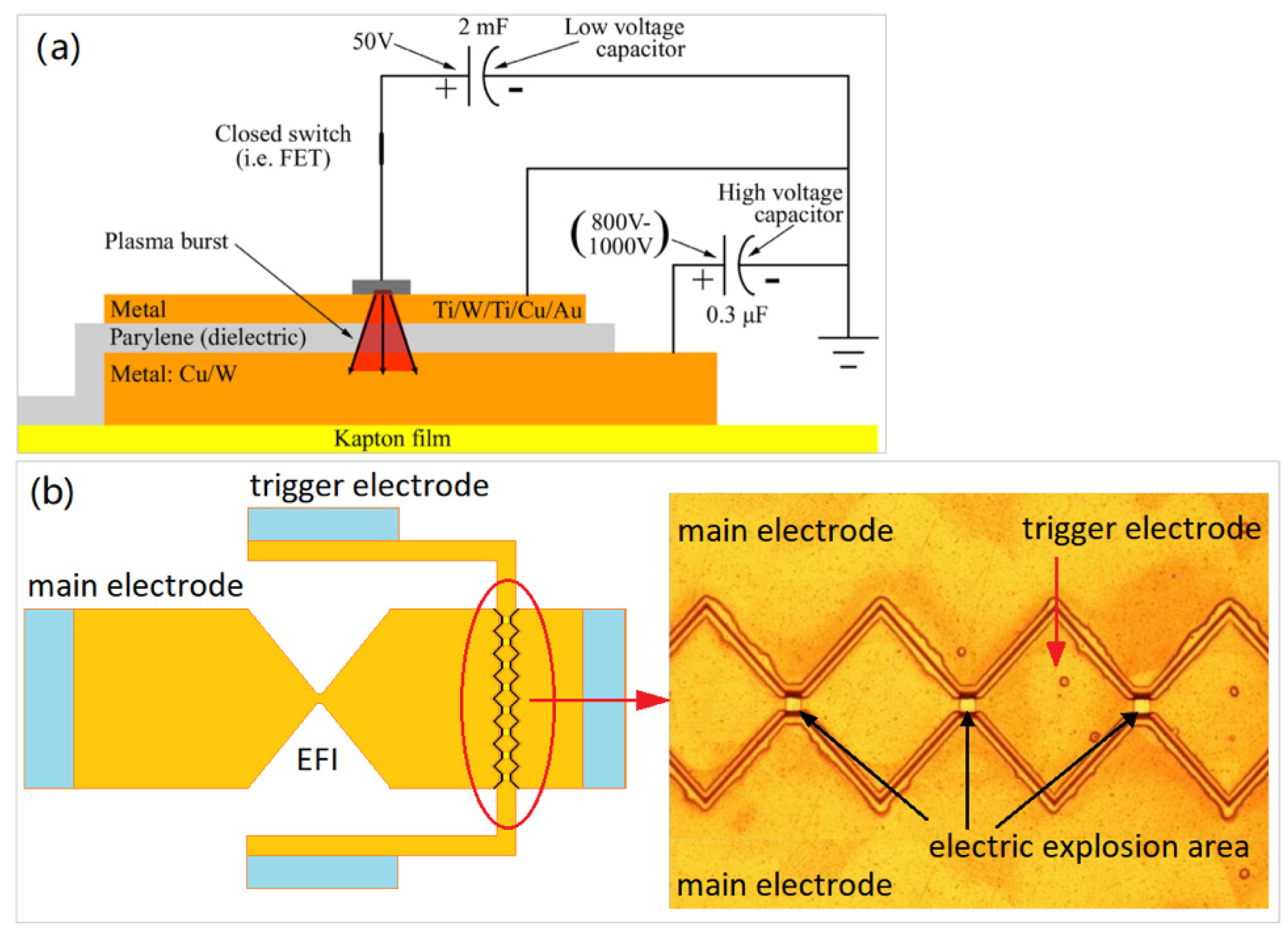
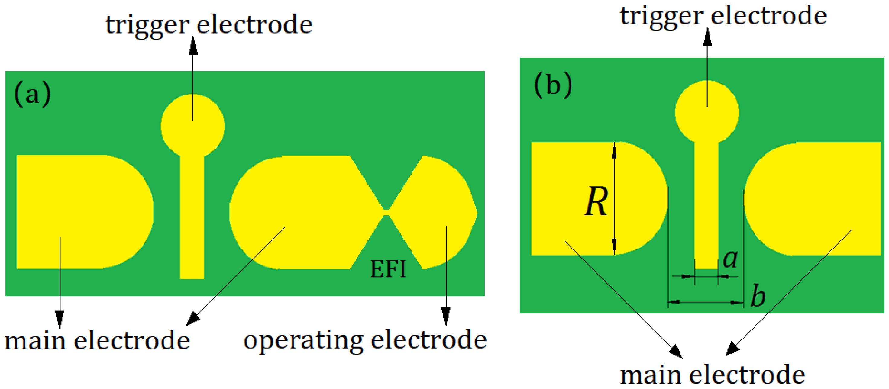
2.1. The Design of Switches

The three-electrode planar spark gap high voltage switch was composed of two main electrodes and trigger. The main electrode includes the cathode and anode, as shown in Figure 1. The main electrode is semicircular in shape and placed in the opposite position. The trigger electrode is located in the middle of the two main electrodes. Its principle is to load high DC voltage between the cathode and anode of the switch. When a specific pulse voltage signal is applied to the trigger electrode, a high voltage gap is formed between the cathode and the trigger electrode. A certain number of ions or electrons are produced by the breakdown field strength, and the particles and gas undergo the collision multiplication process, resulting in the instantaneous conduction of the anode and cathode of the switch. In Figure 3, a represents the width of the trigger electrode, b represents the gap width of the main electrode, and R represents the radius of the main electrode.
As can be seen from Figure 3, the key structures of the planar three-electrode switch include the main electrode radius (R), the main gap (b), the trigger gap ((ba)/2) and the trigger electrode width (a). The diameter R of the two main electrodes is a semi-circular structure with a diameter of 4.0 mm ± 0.5 mm. The purpose of this design is to ensure that a uniform electric field exists between the electrode gaps as much as possible, so as to improve the service life of the switch. With the input of the trigger signal, the switch conduction first occurs in the trigger gap. Therefore, reducing the trigger gap is beneficial to improve the working reliability of the switch, but the gap is too small, which affects the working voltage range and safety of the switch. Combined with the machining accuracy, the structural design parameters for the plane three-electrode spark gap high-voltage switch are shown in Table 1.

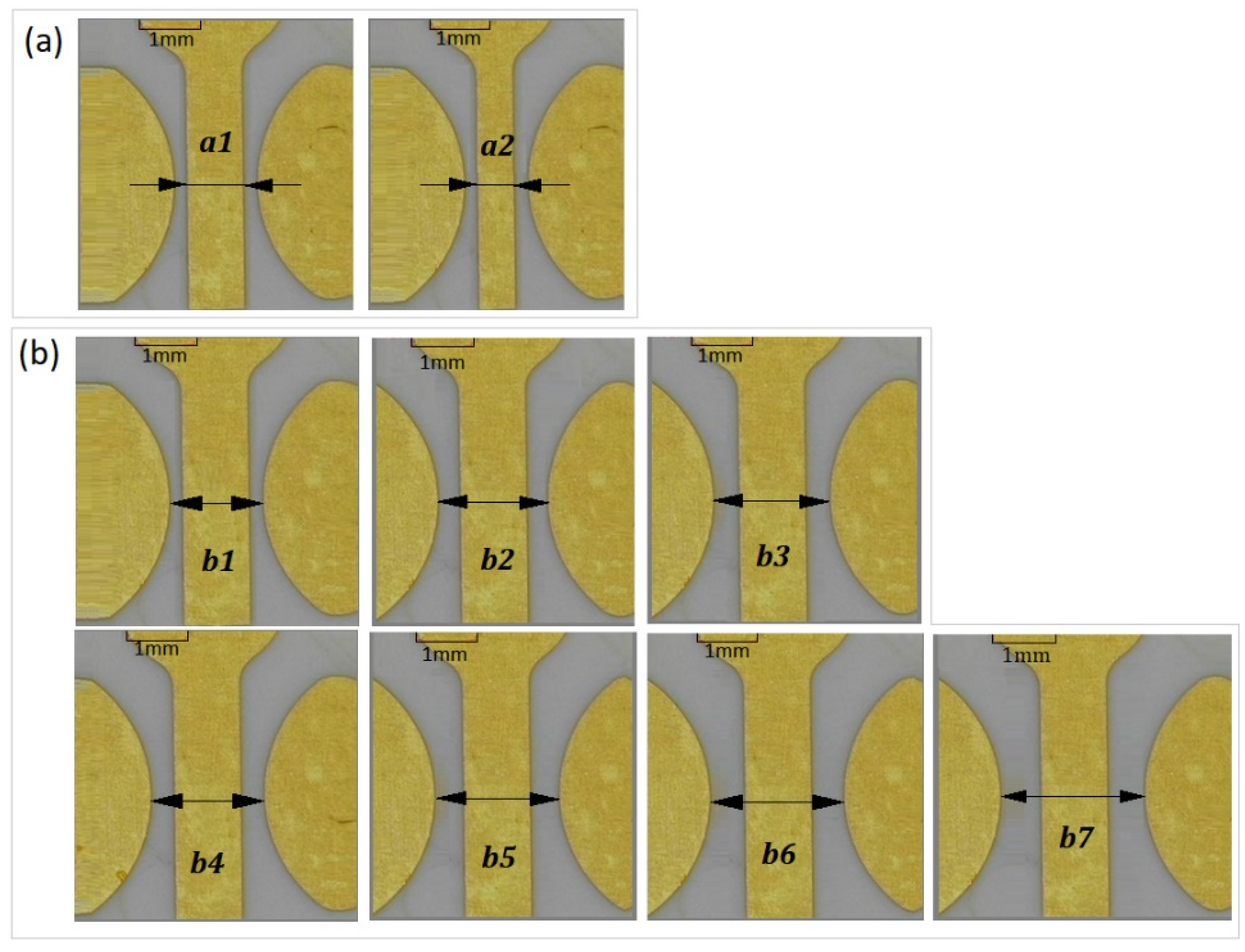
2.2. Switch Fabrication and Characterization

In the three-electrode planar spark gap high voltage switch, a magnetron sputtering coater was used to sputter copper film on the surface of the substrate. The coating photoresist is spined on the surface of the copper film. Then the photoresist surface is covered with a photoresist mask, which is exposed under a strong light to develop the substrate. Finally, the final switch is formed after being etched with FeCl3 etching solution. The switch is shown in Figure 4.
The microscope stage micrometer is used to test the switch structure size according to the parameter requirements in Table 1. The test results are all within the design range requirements.

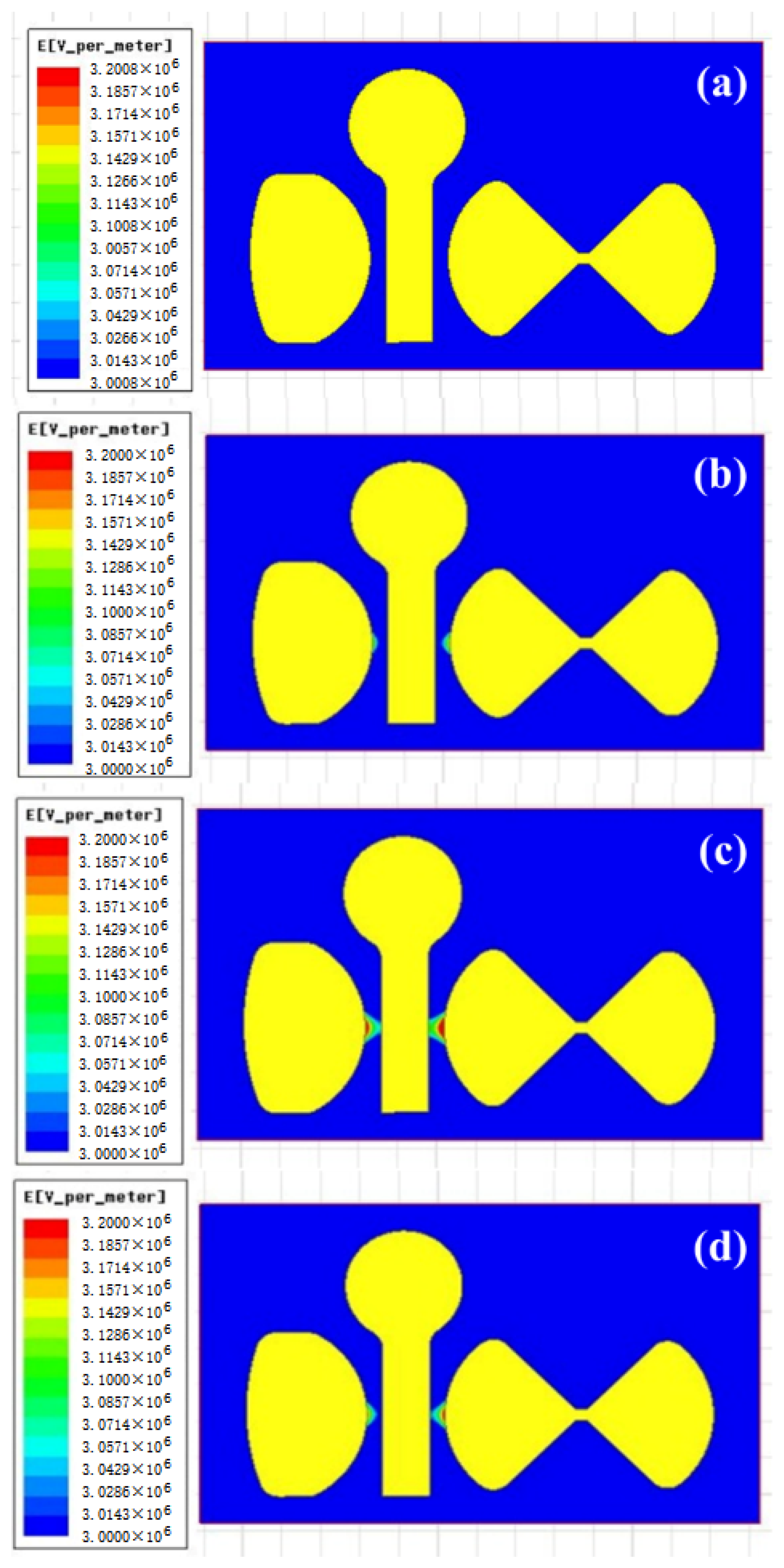
3. Research on the Characteristics of High-Voltage Switching with Three-Electrode Plane Spark Gap

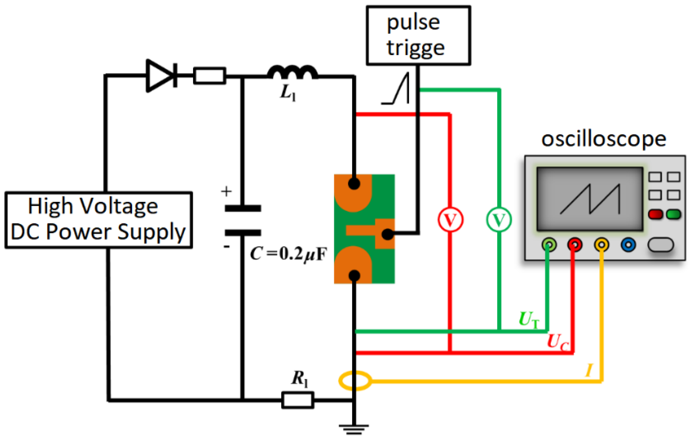
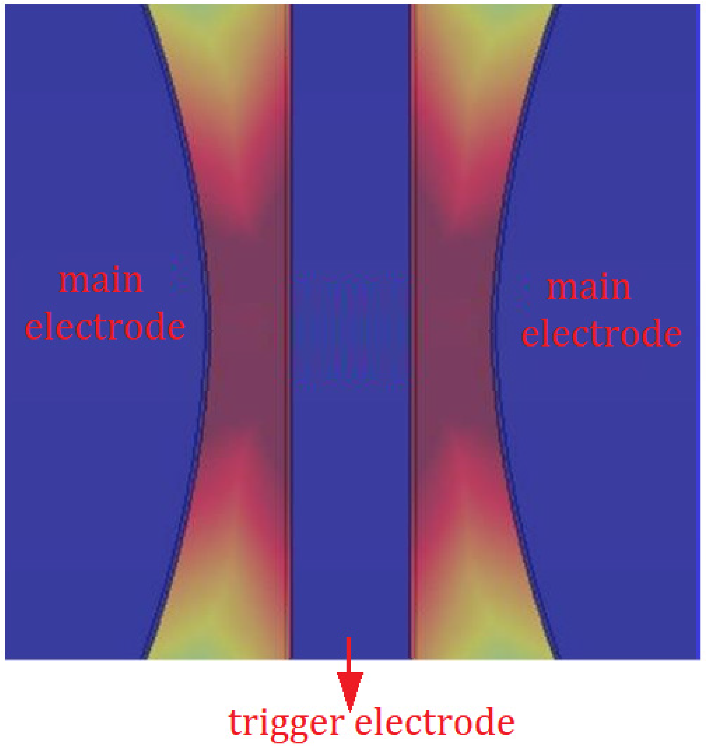
3.1. Test Device and Principle

For the performance test of the three-electrode planar spark gap high-voltage switch, the test device includes a high-voltage power supplied with the output voltage of 0~4 kV and accuracy of 1‰, a pulse trigger power supplied with the adjustable output voltage of 0~3 kV, a rising pulse time of no more than 100 ns and falling pulse time of no more than 1 μs, a digital high-voltage meter with input impedance of 1000 mΩ and measurement accuracy of 1‰, the Rogofiski Roche current measuring coil with the model specification of 5008c, a voltage divider of 1/1000, and a high voltage pulse capacitor with the model specification of C471/0.2 μF/3.0 kV. The test principle is shown in Figure 5.
As shown in Figure 5, the high-voltage DC power supply outputs the working voltage USB to the positive electrode of the high-voltage capacitor and the three-electrode plane spark gap high-voltage switch, and the pulse trigger power supply provides the trigger voltage Utrigger to the three-electrode plane spark-gap high-voltage switch. When the electric field strength between the trigger electrode and the main electrode is greater than the breakdown strength of the air in the gap, a breakdown occurs between the gaps, the electric field in the gap is distorted, and a large number of electrons in the negative electrode of the main electrode rapidly move to the positive electrode to turn on the switch. The high-voltage capacitor discharges the load through the three-electrode plane spark gap high-voltage switch, and uses the Rogowski coil, the high-voltage probe and the voltage divider, and the oscilloscope to test the discharge current, working voltage, and trigger voltage in the loop, respectively.

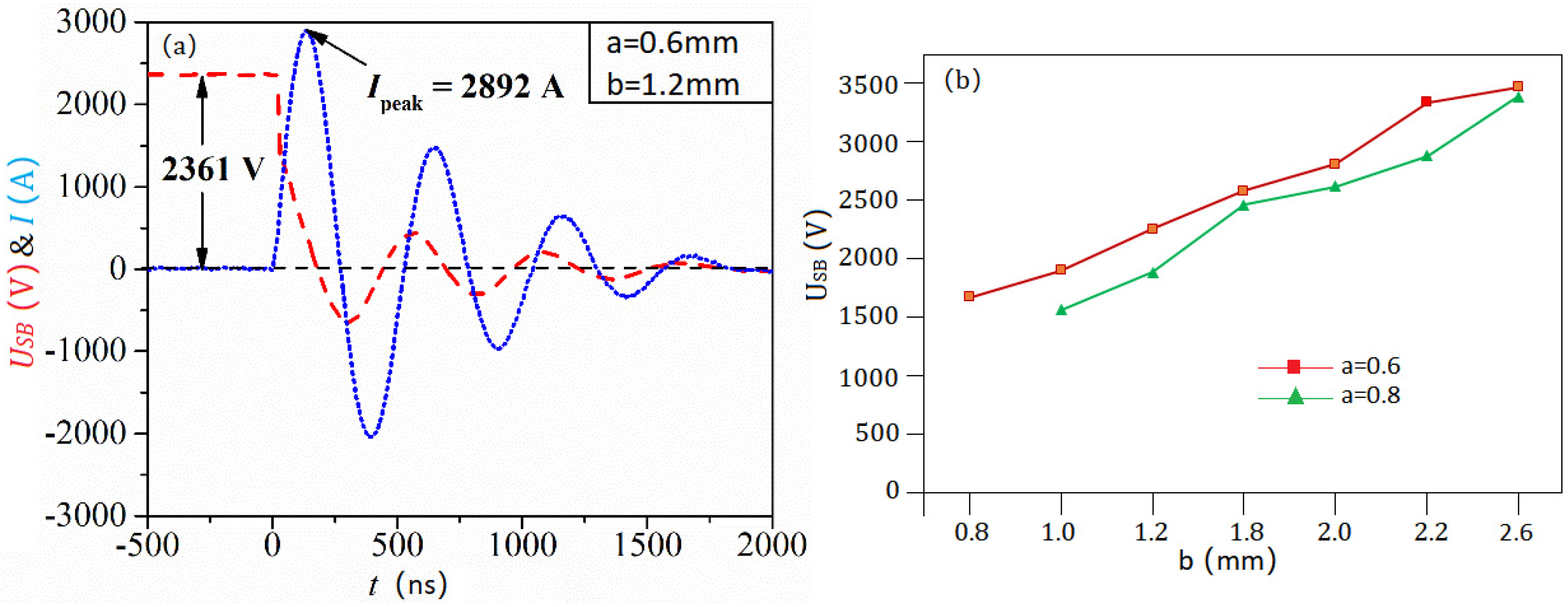
3.2. Static Self-Breakdown Characteristics

The three-electrode planar spark gap high-voltage switch based on copper foil, like other high-voltage switches, needs to have a specific operating voltage range; that is, the gap between the main electrode and the trigger electrode of the switch can withstand a certain high voltage without self-breakdown. Therefore, the self-breakdown voltage USB of the switch is also the maximum working voltage of the switch. The high voltage capacitor (0.2 μF) is slowly charged at a rate of about 20 V/s from the high voltage DC power supply, until the air in the gap between the two electrodes occurs self-breakdown. A high-voltage probe and Rogowski coil were used to record the self-breakdown voltage USB and loop current I changes. When the width a of the trigger electrode is 0.6 mm and the width b of the gap between the two main electrodes is 1.2 mm, the test waveform of the self-breakdown characteristic of the switch is shown in Figure 6a. The maximum operating voltage USB is 2361 V, and the maximum output current peak value is 2892 A. The USB test curves of different parameters of the plane spark gap switch by the orthogonal method are shown in Figure 6b.
It can be seen from Figure 6.b that as the main electrode gap increases from 0.8 mm to 2.6 mm, the self-breakdown voltage of the planar spark gap switch gradually increases, and the operating voltage also increases. When the main electrode gap is a maximum of 2.6 mm, the self-breakdown voltage of the switch can reach 3480 V, which indicates that the maximum operating voltage of the switch is 3480 V. According to Thomson’s theory and Baschen’s law [24,25] of uniform electric field self-discharge under low pressure, the breakdown voltage USB of the air gap is related to the air pressure p and the main electrode gap b, and under the condition of a fixed gas atmosphere, the maximum operating voltage USB is positively correlated with b. By carrying out a large number of self-breakdown characteristic tests, it is shown that the self-breakdown voltage fluctuates greatly (the range is about 180 V), and the larger the gap, the greater the fluctuation. According to the principle of electrostatic discharge, this is because the trigger electrode is right-angled, and tip discharge is prone to occur during the conduction process, which makes the field strength here larger, resulting in an increase in the unevenness of the electric field.

3.3. Dynamic Operating Characteristics

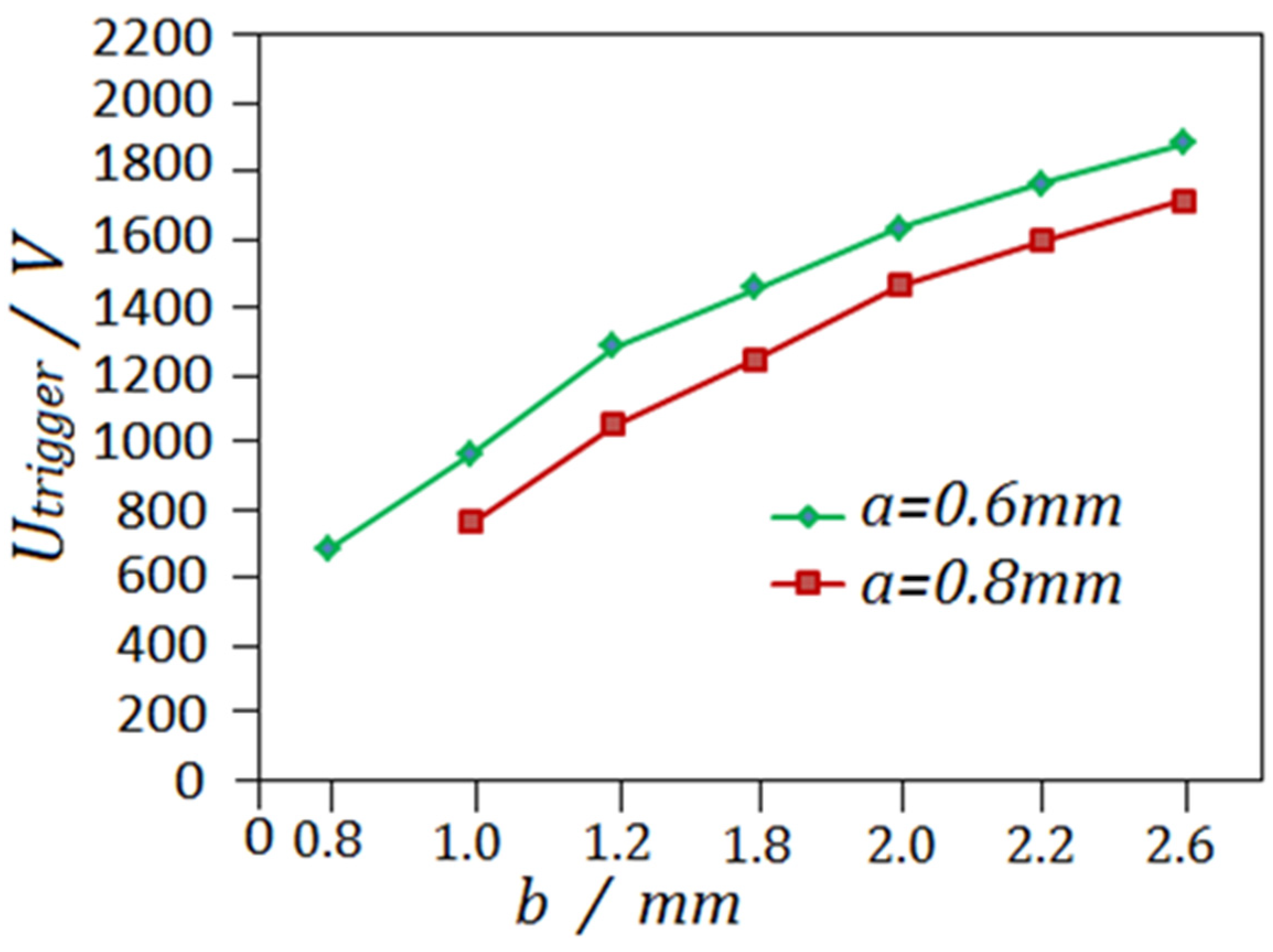
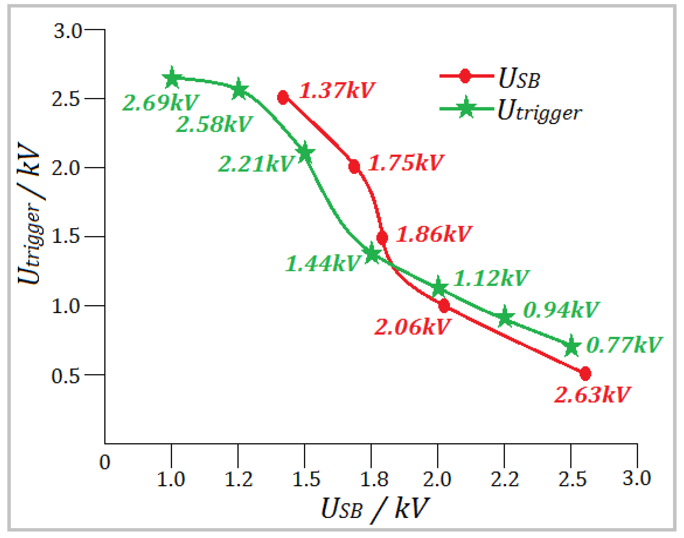
3.3.1. Dynamic Minimum Trigger Voltage

In order to determine the conduction condition of the three-electrode planar spark gap high voltage switch with seven kinds of main electrode gaps, the three-electrode planar spark gap high voltage switch with main electrode gaps of 0.8 mm, 1.0 mm, 1.2 mm, 1.8 mm, 2.0 mm, 2.2 mm, and 2.6 mm are designed, and the trigger electrode widths are 0.6 mm and 0.8 mm, respectively. With the charging voltage of 2.0 kV, the minimum trigger voltage curves of various switch parameters are shown in Figure 7.
As shown in Figure 7, under the condition of charging voltage of 2.0 kV, as the main electrode gap increases from 0.8 mm to 2.6 mm, the minimum trigger voltage value of the planar spark gap switch increases from 677 V to 1783 V (a = 0.6 mm), 685 V rises to 1766 V (a = 0.8 mm). This shows that with the continuous increase of the main electrode gap, the minimum trigger voltage of the switch increases. With the same gap, the width of the trigger electrode is wider, the minimum trigger voltage becomes lower, for the reason that the conduction principle of the three-electrode planar spark gap high voltage switch is to apply pulse trigger voltage to the trigger electrode. Herein, the gap electric field is distorted and the air breakdown effect occurs between the gaps, making the two poles of the switch conduct. When the three-electrode planar spark gap high voltage switch is in the triggering state, the average electric field strength between the two poles is calculated as follows [26,27]:
E = U S B b a
E: Average electric field, V/m;
USB: Working voltage, V;
b: Gap, mm;
a: Trigger electrode width.
As shown in Formula (2), under the condition of the same trigger electrode width, when the applied voltage USB between the two poles is constant, the average electric field strength E increases with the decrease of gap b, meaning that the smaller the gap between the two poles of the switch is, the greater the average electric field strength becomes, and the easier the air gas breakdown effect occurs, so the energy required for the trigger electrode is lower. On the contrary, the average electric field strength between the two poles of the switch is stronger and the energy required for the trigger is higher, when the switch is on. As shown in Formula (2), under the condition of the same gap, when the applied voltage USB between the two poles is fixed, the width of the trigger electrode is increased, the average electric field strength increases, and the air breakdown effect occurs easily, resulting in the lower energy required for the trigger electrode.
The matching test between the working voltage and the trigger voltage was carried out. The test results show that the relationship between the trigger voltage and the working voltage is inversely proportional. When the working voltage was high, the switch turned on easily, and the minimum trigger voltage was reduced. That is because when a relatively high voltage is applied between the two poles of the switch, the average electric field strength increases, and it is easier for breakdown effect to take place between the two poles of the switches, the trigger pole and air interface. Therefore, the required trigger energy will become low. The fitting curve of the relationship between the working voltage of the switch and the trigger voltage was shown in Figure 8.

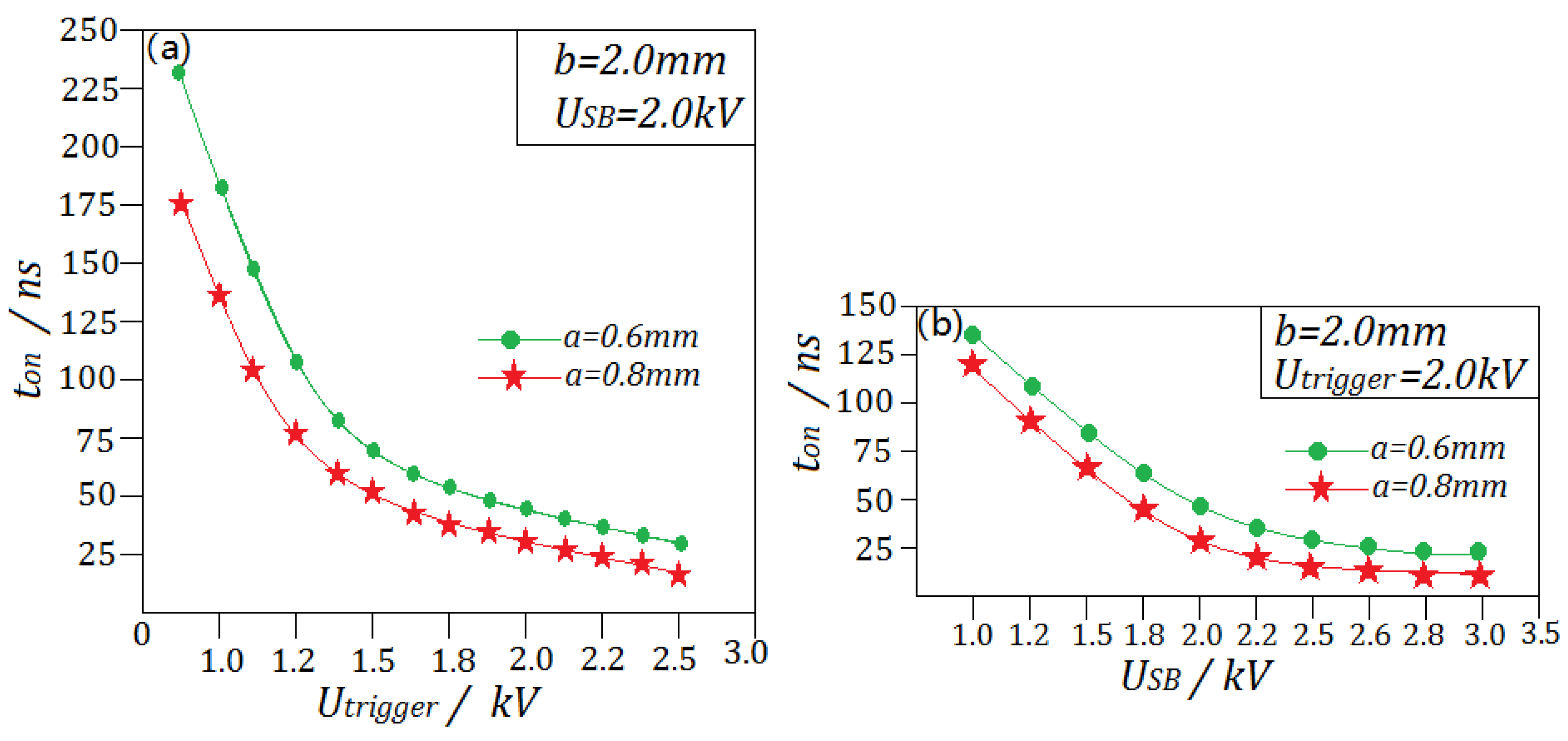
3.3.2. Switch Dynamic Conduction Performance

The time ton is the conduction time of the three-electrode planar spark gap high voltage switch. This is measured from the time when applying the trigger pulse voltage for the trigger electrode to the time when completely connection of the two poles of the switch and the oscillation current occurred in the discharge circuit. When the trigger electrodes are 0.6 mm and 0.8 mm, the trigger voltage is 1.8 kV, and the working voltage is 2.0 kV, the switch on-time ton test results of different gaps are 16 ns, 22 ns, 28 ns, 48 ns, 64 ns, 77 ns, and 93 ns (a = 0.6 mm) and 26 ns, 34 ns, 51 ns, 67 ns, 81 ns, and 102 ns (a = 0.8 mm). The test waveforms are shown in Figure 9.
In Figure 9, the tested waveform of the on-off performance of the switches can be seen. With the increasing gap, the on-off time of the switch becomes gradually longer, and the peak current of the discharge circuit is reduced. When the switch is on, the breakdown effect starts between the pulse trigger voltage and the strong electric field with the air interface, resulting in the electric field distortion between the two poles of the switches. A certain number of ions or electrons are generated instantaneously and move with a high speed under the electric field of the two poles of the switch. When the working voltage, trigger voltage, and the width of trigger electrode are fixed, with the increase of the switch gap, the average electric field strength between the two poles of the switch decreases, which leads to the decrease of the velocity of ions or electrons generated when the switch is on, so that the on-time of the switch becomes longer. On the contrary, when the switch gap is low, with the increase of the average electric field, the average electric field strength between the two poles of the switch decreases, the velocity of ions or electrons increases and the on-time decreases. In addition, with the increase of the gap between the two poles of the switch, the average electric field strength between the two poles of the switch decreases. When the breakdown effect occurs between the trigger pole and the air interface, the energy loss is large, leading to a decrease in the peak current in the circuit. The regular curves between the trigger voltage and operating voltage of the switch and the on-time of the switch are shown in Figure 10.

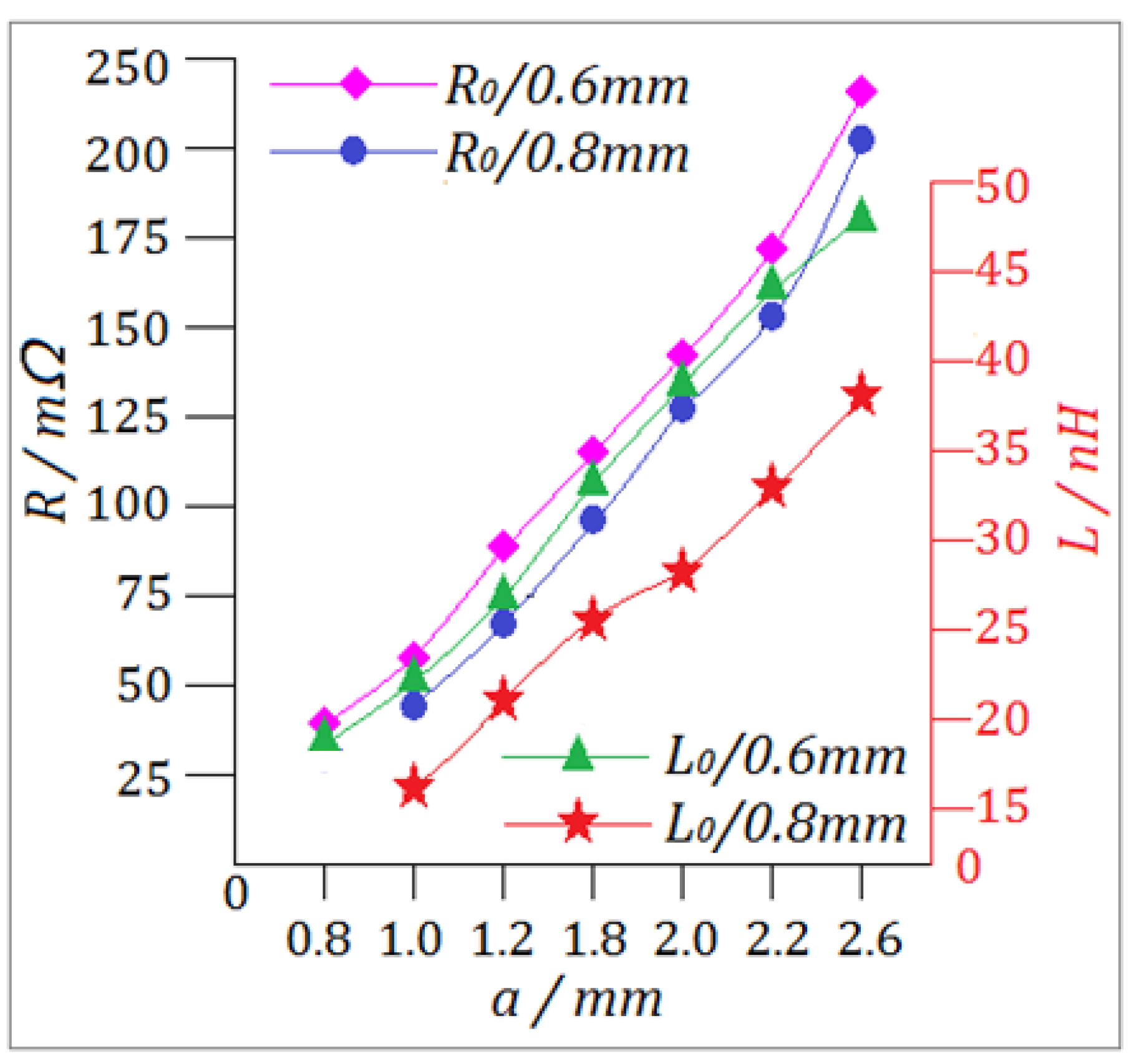
3.3.3. Switch Dynamic Impedance and Inductive Reactance Characteristics

In order to realize the function of switching and disconnecting the narrow pulse current in the exploding foil initiation circuit, the high voltage switch not only has a higher turn-off impedance to reduce the power consumption of the exploding foil initiation system, but also has a lower conductive impedance and inductive reactance to improve the narrow pulse current output characteristics of the high-voltage pulse capacitor.
In principle, the initiation circuit of exploding foil can be equivalent to a RLC series circuit [28,29,30]. The parasitic resistance and inductance of the three-electrode planar spark gap high voltage switch can be calculated by measuring the waveform parameters of discharge oscillation current of the circuit with oscilloscope.
The formula of parasitic inductance is as follows.
L 0 = L l
L = T ¯ 2 4 π 2 C
The formula of parasitic resistance is as follows.
R 0 = R r
R = 2 L T ¯ ln ξ ,   among   them ,   ξ = j = 1 n λ j n ,   λ j = I j I j + 1
L: Total inductance of discharge circuit, nH;
l: Load inductance, nH;
R: Total resistance of discharge circuit, mΩ;
r: Load resistance, mΩ;
T ¯ : The average period of oscillation, µs;
Ij+1, Ij: The value of forward oscillation current, kA;
ξ : The average coefficient of current attenuation;
C: High voltage pulse capacitance, µF;
According to the test and calculation results, the corresponding data of the relationship between the gaps of two main electrodes, the width of trigger electrode, the dynamic impedance, and inductive reactance of the switch are shown in Table 2 and Table 3, and the corresponding curves are shown in Figure 11.
As shown in Figure 11 and Table 2 and Table 3, with the increase of the gap between the two main electrodes of the switches, the dynamic impedance and inductive reactance of the switches is increased, but they will decrease with the increase of the width of the trigger electrode. The increase range of impedance relativity is larger than that of the inductive reactance. With the increase of the gap between the two main electrodes of the switch, the average electric field strength between the two main electrodes had been reduced and the concentration of ions or electrons had been decreased, resulting in the decrease of electric current density passing through. Therefore, the impedance and inductive reactance will increase. As the width of trigger electrode increased, the gap between the two main electrodes becomes smaller and the average electric field strength between two main electrodes increases, resulting in lower impedance and inductive reactance.

3.4. Discharge Life Characteristics of Planar Spark Gap Switch

The service life of the high-voltage switch seriously affects the working reliability of the exploding foil initiation system. The performance of the three-electrode planar spark-gap high-voltage switch based on copper foil was reduced after several discharge tests. Under the same input voltage condition, the working reliability is reduced, the conduction time is longer, and the trigger voltage needs to be increased. Moreover, it was found that the trigger electrode of the switch had traces of burns, as shown in Figure 12.
After analysis, this is because the electrode gap is filled with air, so that the three-electrode planar spark gap switch can withstand a specific high voltage, but when the switch needs to be triggered and turned on, it needs to form a sufficient electric field strength in the trigger gap. Since the thickness of the copper foil-based three-electrode plane spark gap high-voltage switch is only 4.0 μm, a large amount of ions or electrons will be generated in the instant when the switch is turned on, and the narrow pulse strong current generated by the discharge circuit will be turned on, causing burns to the switch electrodes.
The electrode thickness of the three-electrode plane spark gap switch has a certain influence on the field strength, and ultimately affects the service life of the switch. The electrostatic field of the three-electrode plane switch is analyzed with the help of finite element simulation software. In the simulation, copper was selected as the electrode material, and air was selected as the dielectric material. The excitation source was electrostatic field solver excitation source, and the boundary condition is balloon boundary condition. The diameter of positive and negative main electrodes is 4.0 mm, the distance b is 2.0 mm and the width of trigger electrode a is 1.2 mm. The setting negative voltage is 0 V, the positive voltage is 1.3 kV, the trigger voltage is 1.5 kV, the number of calculation steps is 10, and the allowable error is 0.1%. Figure 13 shows the overall field intensity distribution cloud diagram of the three-electrode plane spark gap high voltage switch, Figure 14 shows the electric field distribution before triggering, and Figure 15 shows the electric field distribution after triggering.
As shown in Figure 14, when a high voltage of 1.3 kV is provided between the two main electrodes of the switch, the electric field is evenly distributed between the two main electrodes, and the field strength near the edge of the trigger electrode is the largest at 22.9 kV/cm. At this time, the maximum field strength is lower than the breakdown strength of air by 30 kV/cm, so the switch cannot self-breakdown. Considering that the air in the test environment is a non-ideal environment, the breakdown strength of the air will be lower than the ideal 30 kV/cm due to factors such as humidity and temperature. In order to improve the safety of the switch, it is necessary to reserve a certain distance to ensure the insulation effect and avoid false triggering. As shown in Figure 15, the trigger electrode was applied with a voltage of 1.5 kV, and the maximum electric field strength between the trigger electrode and the cathode reached 52.5 kV/cm, which was 30 kV/cm higher than the breakdown strength of air. At this time, the gas between the trigger electrode and the cathode will be ionized, and electrical breakdown will occur, so that the main electrodes will be broken down, and the conduction loop will discharge. In order to improve the working reliability of the switch, when the trigger voltage is loaded, the minimum electric field strength between the two main electrodes and the trigger electrode must be higher than the breakdown strength of air by 30 kV/cm.
The maximum static operating voltage of the three-electrode planar switch is simulated by the established simulation model. In the simulation, the dielectric material is air, no trigger voltage is applied, the negative voltage is 0 V, and the anode voltage constantly increases from 0 V. When the electric field strength of the main electrode gap is greater than the air breakdown strength, the switch is considered to be broken down. Since the breakdown strength of ideal air is 30 kV/cm, the lower limit of the field strength is set to 30 kV/cm in the simulation results; only the electric field strength greater than the breakdown strength of air is displayed, so that the self-breakdown process of the switch can be visually observed, and the self-breakdown voltage can be obtained, as shown in Figure 16.
Figure 17 is a partial enlarged view of the field strength of the switch gap. It can be seen from Figure 17 that the field strength of the trigger gap has increased significantly, and the field strength is greater as it is closer to the trigger electrode. The electrostatic field simulation results show that the discharge first occurs in the trigger gap, and then extends to the entire main electrode gap, but the field strength is the highest around the main electrode closest to the trigger electrode, and a high concentration of electron clouds appears. However, since the thickness of the switch electrode is only 4 μm, a burning phenomenon occurs.

4. Conclusions

In view of the low-energy explosion foil detonation system’s requirements for the integration technology of high-voltage switches and the technical overload resistance technology, a magnetron sputtering coater is used to sputter copper film on the surface of the substrate. The thickness is 4.0 μm, the radius of the main electrode is 4 mm, the trigger electrode is 0.6 mm and 0.8 mm, and the main gaps are 0.8 mm, 1.0 mm, 1.2 mm mm, 1.8 mm, 2.0 mm, 2.2 mm, and 2.6 mm. Copper foil three-electrode planar spark gap high voltage switches are designed and manufactured, and the static self-breakdown characteristics, dynamic operating characteristics, and discharge life characteristics of the three-electrode planar spark gap high voltage switch based on copper foil are studied in this paper. The test results show that with the increase of the main electrode gap from 0.8 mm to 2.6 mm, the self-breakdown voltage of the planar spark gap switch increases, and the working voltage also increases. When the main electrode gap is a maximum of 2.6 mm, the self-breakdown voltage of the switch can reach 3480 V, which indicates that the maximum operating voltage of the switch is 3480 V. Under the condition of charging voltage of 2.0 kV, with the increase of the main electrode gap from 0.8 mm to 2.6 mm, the minimum trigger voltage value of the planar spark gap switch increases from 677 V to 1783 V (a = 0.6 mm), and from 685 V to 1766 V (a = 0.8 mm), the switch-on times are 16 ns, 22 ns, 28 ns, 48 ns, 64 ns, 77 ns, 93 ns (a = 0.6 mm), and 26 ns, 34 ns, 51 ns, 67 ns, 81 ns, 102 ns (a = 0.6 mm). With the increase of the main electrode gap, the maximum static operating voltage of the three-electrode planar spark gap high voltage switch increased. When the same width of trigger electrode was used, the minimum trigger voltage increased, with the increase of the main electrode gap. When the same width of the trigger electrode was used, the minimum trigger voltage decreased. When the switch had the same parameters, the trigger voltage was inversely proportional to the working voltage. When the same width of the trigger electrode was used, with the increase of the gap between main electrodes, the conduction time of the switch was longer, and the peak current of the discharging circuit decreased. The dynamic impedance and inductive reactance of the switch increase with the increase of the gap between the two main electrodes, and decrease with the increase of the width of the trigger electrode.

Author Contributions

Conceptualization, K.H., Q.J. and E.C.; methodology, K.H. and W.Z.; software, P.D. and K.H.; validation, K.H. and W.Z.; formal analysis, W.Z. and Q.J.; investigation, K.H., Q.J. and E.C.; resources, E.C. and K.H.; data curation, K.H., W.Z. and Q.J.; writing—original draft preparation, K.H., W.Z. and Q.J.; writing—review and editing, K.H., W.Z. and Q.J.; visualization, P.D. and K.H.; supervision, Q.J. and E.C.; project administration, Q.J. and E.C.; funding acquisition, K.H. and W.Z. All authors have read and agreed to the published version of the manuscript.

Funding

We appreciate the funding support from the National Natural Science Foundation of China (Grant No. 22105025 and Grant No. 52022013). Thanks for the support from the China Postdoctoral Science Foundation (Grant No. 2021M690376).

Institutional Review Board Statement

Not applicable.

Informed Consent Statement

Not applicable.

Data Availability Statement

Not applicable.

Conflicts of Interest

The authors declare no conflict of interest. The founding sponsors had no role in the design of the study; in the collection, analyses, or interpretation of data; in the writing of the manuscript, and in the decision to publish the results.

References

  1. Strand, T.; Berzins, L.V.; Goosmanl, D.R. Velocimetry using heterodyne techniques. In Proceedings of the 26th International Congress on High-Speed Photography and Photonics, Alexandria, VA, USA, 20–24 September 2004; pp. 593–599. [Google Scholar]
  2. Prinse, W.; Scholtes, G. A Development Platform for a Microchip EFI. In Proceedings of the 52nd Annual Fuze Conference, Sparks, NV, USA, 13–15 May 2008. [Google Scholar]
  3. Han, K.-h.; Zhou, J.; Rec, X.; Liu, T.; Ao, C.-g.; Tong, H.-h. Effect of High Voltage Pulse Power Source Equivalent Parameter on Exploding Performance of Foil Bridge. Hanneng Cailiao/Chin. J. Energ. Mater. 2014, 22, 828–833. [Google Scholar]
  4. Chu, K.W.; Scott, G.L. A Comparison of High-Voltage Switches; Sandia National Labs.: Albuquerque, NM, USA; Livermore, CA, USA, 1999. [Google Scholar]
  5. Jim, R.D. Fireset for a Low Energy Exploding Foil Initiator: SCR Drive MOSFET Switch. US Patent 6138571, 31 October 2000. [Google Scholar]
  6. Xu, C.; Zhu, P.; Chen, K.; Zhang, W.; Shen, R.; Ye, Y. A highly integrated conjoined single shot switch and exploding foil initiator chip based on MEMS technology. IEEE Electron Device Lett. 2017, 38, 1610–1613. [Google Scholar] [CrossRef]
  7. Yang, Z.; Wang, K.; Zhu, P.; Liu, P.; Zhang, Q.; Xu, C.; Jian, H.T.; Shen, R.Q. A reusable planar triggered spark-gap switch batched-fabricated with PCB technology for medium-and low-voltage pulse power systems. Defence Technol. 2021, 17, 1572–1578. [Google Scholar] [CrossRef]
  8. Fujii, K.; Koellensperger, P.; Doncker, R. Characterization and comparison of high blocking voltage IGBTs and IEGTs under hard- and soft-switching conditions. IEEE Trans. Power Electron. 2008, 23, 172–179. [Google Scholar] [CrossRef]
  9. Hanks, R.L. Low-Jitter High-Power Thyristor Array Pulse Driver and Generator. US Patent 6462605 B1, 8 October 2002. [Google Scholar]
  10. Salyers, P. Guided MLRS electronic safety & arming devices (ESAD) & electronic safety& arming fuze (ESAF). In Proceedings of the 43rd Gun & Missile Conference, NAIA, New Orleans, LA, USA, 21–24 April 2008. [Google Scholar]
  11. Soto, G. Navy Overview. In Proceedings of the 59th Annual Fuze Conference, Charleston, SC, USA, 4 May 2016. [Google Scholar]
  12. Graham, R.A. Shock-induced electrical switching in polymeric films. In Mega-Gauss Physics and Technology; Springer: New York, NY, USA, 1980. [Google Scholar]
  13. Richardson, D.D. The Effect of Switch Resistance on the Ring down of a Slapper Detonator Fireset; MRL-R1004; Materials Research Laboratories: Struthers, OH, USA, 1986. [Google Scholar]
  14. Nerheim, E. Integrated Silicon Plasma Switch. US Patent 4840122, 20 June 1989. [Google Scholar]
  15. Han, K.; Deng, P.; Chu, E.; Jiao, Q. Effect of Grain Size and Micromorphology of Cu Foil on the Velocity of Flyer of Exploding Foil Detonator. Appl. Sci. 2021, 11, 6598. [Google Scholar] [CrossRef]
  16. Baginski, T.A.; Thomas, K.A. A Robust One-Shot Switch for High-Power Pulse Applications [EB/OL]. IEEE Trans. Power Electron. 2009, 24, 253–259. [Google Scholar] [CrossRef]
  17. Baginski, T.A.; Dean, R.N.; Wild, E.J. Micromachined planar triggered spark gap switch. IEEE Trans. Compon. Packag. Manuf. Technol. 2011, 1, 1480–1485. [Google Scholar] [CrossRef]
  18. Zhou, M.; Meng, Q.Y.; Han, K.H.; Qian, Y.; Qin, G.S. Design and research on exploding plane switch. Initiat. Pyrotech. 2012, 12–14. Available online: https://en.cnki.com.cn/Article_en/CJFDTotal-HGPI201206005.htm (accessed on 30 December 2012).
  19. Wang, R.; Cheng, T.; Zhang, Y. Research on Voltage Resistance Performance of Micro-sized Exploding Foil Plane Discharge Switch. Initiat. Pyrotech. 2018, 1–4. Available online: https://caod.oriprobe.com/issues/1836321/toc.htm (accessed on 30 August 2018).
  20. Li, J.; Jiao, Q.; Chu, E.; Chen, J.; Ren, W.; Li, K.; Tong, H.; Yin, G.; Wang, Y.; Zhou, M. Design, fabrication, and characterization of the modular integrated exploding foil initiator system based on low temperature co-fired ceramic technology. Sens. Actuators A Phys. 2020, 315, 112365. [Google Scholar] [CrossRef]
  21. Xu, C.; Zhu, P.; Zhang, W.; Shen, R.; Ye, Y. A plasma switch induced by electro-explosion of p-n junction for mini exploding foil initiator. IEEE Trans. Plasma Sci. 2019, 47, 2710–2716. [Google Scholar] [CrossRef]
  22. Xu, C.; Zhu, P.; Wang, K.; Qin, X.; Zhang, Q.; Yang, Z.; Shen, R. An electro-explosively actuated mini-flyer launcher. Sens. Actuators A Phys. 2019, 292, 17–23. [Google Scholar] [CrossRef]
  23. Xu, C.; Zhu, P.; Zhang, Q.; Yang, Z.; Wang, K.; Shen, R. A shock-induced pulse power switch utilizing electro-explosion of exploding bridge wire. IEEE Trans. Power Electron. 2020, 35, 10770–10777. [Google Scholar] [CrossRef]
  24. Peitian, C.; Aici, Q. Review on gas switches developed for fast linear transformer driver. High Power Laser Part. Beams 2012, 24, 1263–1268. [Google Scholar] [CrossRef]
  25. Jiang, X.; Cong, P.; Sun, F.; Sun, T.; Liang, T.; Wei, H.; Wang, Z. Breakdown characteristics of a multi-gap gas switch with corona discharge for voltage balance. High Power Laser Part. Beams 2016, 28, 075009. [Google Scholar]
  26. Chen, Q.; Li, Y.; Ma, T. Characterization of the super-short shock pulse generated by an exploding foil initiator. Sens. Actuators A Phys. 2019, 286, 91–97. [Google Scholar] [CrossRef]
  27. Hu, B.; Jiao, J.; Zhu, P.; Wu, L.; Ye, Y.; Shen, R. Characterization of electrical explosion of schottky diode for one-shot switch applications. Eur. Phys. J.-Appl. Phys. 2014, 68, 30801. [Google Scholar] [CrossRef]
  28. Liu, C.; Yang, Z.; Ding, G.; Zhou, Z.; Liu, Q.; Huang, Y.; Zheng, Y. Design, simulation, and Characterization of a low-cost in-plane spark gap microswich with dual-trigger electrode for pulsed power applications. IEEE Trans Ind. Electrtonics 2013, 60, 3240–3247. [Google Scholar] [CrossRef]
  29. Baginski, M.E.; Shaffer, E.C.; Thomas, K.A.; McGuirk, J.S. Acomparison of the electrodynamics of metals under the action of large electric currents. Int. J. Appl. Electromagn. Mech. 2000, 11, 77–91. [Google Scholar] [CrossRef]
  30. Lovri, M.; Schloz, F. A model for the propagation of a redox reaction through microcrystals. Solid State Elect. Through Microcryst. 1997, 1, 108–113. [Google Scholar] [CrossRef]
Figure 1. Schematic representation of planar-electric explosion switch based on silicon substrate.
Applsci 12 01989 g001
Figure 2. Schematic representation of planar high-voltage switch with SBD trigger and planar-electric explosion switch with series structure. (a) Planar high-voltage switch with SBD trigger. (b) Planar-electric explosion switch with series structure.
Applsci 12 01989 g002
Figure 3. Integrated exploding foil initiator based on three-electrode planar spark gap high-voltage switch. (a) Copper foil three-electrode planar spark-gap high-voltage switch integrated with EFI. (b) Three-electrode planar spark-gap high-voltage switch based on copper foil.
Applsci 12 01989 g003
Figure 4. Physical diagram of three-electrode plane spark gap high-voltage switch. (a) Planar switching with different trigger electrodes. (b) Planar switching with different main electrode gaps.
Applsci 12 01989 g004
Figure 5. Schematic diagram of test principle.
Applsci 12 01989 g005
Figure 6. Waveform and curve of self-breakdown characteristic of three-electrode planar switch. (a) Self-breakdown characteristic waveform (C = 0.2 μF) Figure. (b) Self-breakdown characteristic curve.
Applsci 12 01989 g006
Figure 7. The curves of minimum trigger voltage varying with gap.
Applsci 12 01989 g007
Figure 8. Relation curves between trigger voltage and working voltage.
Applsci 12 01989 g008
Figure 9. The tested waveform of switch conduction performance (a) b = 0.8 mm, (b) b = 1.0 mm, (c) b = 1.2 mm, (d) b = 1.8 mm, (e) b = 2.0 mm, (f) b = 2.2 mm, (g) b = 2.6 mm.
Applsci 12 01989 g009
Figure 10. Curve of factors affecting the conduction time of the three-electrode plane spark gap high-voltage switch. (a) Trigger voltage and on-time relationship curve. (b) Working voltage and on-time relationship curve.
Applsci 12 01989 g010
Figure 11. Corresponding curves of switch parameters with dynamic impedance and inductive reactance of the switch.
Applsci 12 01989 g011
Figure 12. Photo of ablation after switch discharge.
Applsci 12 01989 g012
Figure 13. Cloud diagram of the overall field intensity distribution of the three-electrode plane spark gap high-voltage switch.
Applsci 12 01989 g013
Figure 14. Electric field distribution before triggering.
Applsci 12 01989 g014
Figure 15. Electric field distribution after triggering.
Applsci 12 01989 g015
Figure 16. Electric field distribution of integrated components under different charging voltages (a) electric field distribution at 1500 V, (b) electric field distribution at 1500 V, (c) electric field distribution at 2500 V, (d) electric field distribution at 2500 V, (d) Electric field distribution at 2558 V.
Applsci 12 01989 g016
Figure 17. Simulation results of the field strength distribution in the trigger gap of the three-electrode plane spark gap high-voltage switch.
Applsci 12 01989 g017
Table 1. Switch Structure Parameters.
Structure NameCodeParameter
Switch thicknessd4 μm ± 0.1 μm
main electrode radiusR4.0 mm ± 0.5 mm
main gapb0.8/1.0/1.2/1.8/2.0/2.2/2.6 mm
Trigger electrode widtha0.6/0.8 mm
Trigger gap(b − a)/20.1/0.2/0.3/0.6/0.7/0.8/1.0 mm
0.1/0.2/0.5/0.6/0.7/0.9 mm
Table 2. The conductive impedance data of the switch.
b/mm0.81.01.21.82.02.22.6
R0/mΩ
a/mm0.632.851.288.4117.2133.1171.8223.9
0.8/42.768.596.7127.0153.9207.1
Table 3. The inductive reactance data of conductive switch.
b/mm0.81.01.21.82.02.22.6
L0/nH
a/mm0.619.321.829.433.738.242.645.3
0.8/16.619.123.526.230.237.6
Publisher’s Note: MDPI stays neutral with regard to jurisdictional claims in published maps and institutional affiliations.

