1. Introduction
Electrical stimulation, or controlled delivery of electrical pulses to the human body, has been proven to be a beneficial instrument in a variety of applications, such as neuromotor rehabilitation [
1,
2,
3], neuromodulation for tremor suppression and electro-analgesia [
4], cosmetics [
5,
6], sports [
7,
8], wound healing [
9,
10] and drug delivery [
11,
12]. Furthermore, recent advancements in electrical stimulation technologies have opened the possibility of their use in emerging fields such as control of multi-degree of freedom (DoF) prosthetic limbs [
13], telemanipulation tasks [
14], biofeedback [
15] and even interaction with virtual reality [
16].
While the used systems vary from application to application, the common goal is controlled propagation of the electrical current through the human skin and subsequent activation of the targeted neural structures. This is mostly influenced by the shape and placement site of the biomedical electrodes. The challenge is that the optimal electrode configuration is dependent on multivariable factors such as the electrode–skin interface, the skin impedance, and the physical characteristics of the underlying structures. Thus, it is person-specific and can change daily for each person, requiring long set-up times or even expert knowledge for effective application [
17].
Multi-pad electrodes have been proven to be an effective approach to achieve dynamic changes of the shape, size and configuration of the electrodes and as such have been used to address naturally occurring variability in biological systems [
1]. They comprise a matrix of independent pads that can be grouped into subsets, named virtual electrodes, where the pads can be activated in a sequence or simultaneously. By allowing a programmable interface to alter the active electrode surface and position, multi-pad electrodes provide a solution for control of current propagation personalized to each user [
18].
The size and resolution of the virtual electrodes that can be produced is primarily determined by the number of pads in the electrode. However, this number is limited in the state-of-the-art systems. As both the stimulation source and the switching logic are all in the external device (the stimulator), each pad needs an output channel on the stimulation device and an input lead to the electrode. As the number of pads grows, so does the complexity of such systems, making them increasingly cumbersome for production and use and imposing a hard practical limit on the manageable number of pads.
To address this issue and facilitate a drastic increase in the number of pads, we propose a method for migration of the active electronic components responsible for pad selection and configuration into the multi-pad electrode by leveraging the technology of screen-printed organic electrochemical transistors (OECTs).
It has previously been demonstrated that screen-printed OECT-based circuits can be used to reduce the input/output (I/O) number on the external addressing electronic circuits [
19]. This can be achieved by screen-printing various kinds of logic circuits that interpret the input signals provided by the external electronics. For example, two addressing bits in a 2–4 decoder can be provided by the external electronics, and the printed 2–4 decoder circuit ensures that proper addressing of its four output channels is achieved. By using such an attempt in a multi-pad electrode, it is therefore possible to lower the number of leads connected with the electrode pads. A screen-printed shift register is another possible circuit that can be used to lower the I/O count from the addressing electronics to a minimum level. For example, in a 4-bit serial in–parallel out shift register, addressing of the electrodes in the multi-pad electrode is achieved by only using a clock signal and a data input signal. In fact, an arbitrary number of electrode pads can be addressed by using such shift register circuits, thereby lowering the number of leads required between the addressing electronics and the electrode pads.
The screen-printed OECT technology shows several advantages for further utilization in multi-pad electrodes. First of all, it is very robust technology that allows for high manufacturing yields despite using a relatively rough fabrication method in the form of conventional screen printing. This was demonstrated in a previous report, in which reproducible switching characteristics (transfer, output and dynamic measurements) and a manufacturing yield of at least 99.7% were achieved upon evaluating almost 1000 OECTs screen-printed on a relatively large substrate with the dimensions of approximately 200 × 300 mm [
20]. This is mainly due to the electrolytic interface between the gate electrode and the OECT channel. In field effect-driven electronic devices, the voltage drop occurs across the complete thickness of the dielectric layer, and it is therefore critical to deposit very thin layers to obtain low-voltage operation. However, here, in the case of electrolyte-gated devices, the voltage drop occurs at the interfaces between the electrolyte and the gate electrode as well as between the electrolyte and the OECT channel. This ensures low-voltage operation (~1 V) without the requirement of thin layer deposition. The conducting polymer poly(3,4-ethylenedioxythiophene) doped with poly(styrenesulfonate), abbreviated PEDOT:PSS, is used as the active OECT channel material in the devices reported herein. PEDOT:PSS is intrinsically conducting and therefore transports charges throughout the complete thickness of the channel which, in comparison with field effect transistors, implies much higher current levels in the ON state of the OECT. The thickness of the electrolyte layer in screen-printed OECTs often exceeds 10–20 µm, which dramatically simplifies the manufacturing process and hence also implies an increased manufacturing yield. Screen-printed OECT devices have already shown promising results in applications requiring high loads (e.g., as addressing devices used to drive light emitting diodes) [
21] and are therefore a good candidate for switching devices capable of delivering the high current levels needed in multi-pad electrodes for stimulation applications.
The main functional disadvantage of the screen-printed OECT technology is the relatively long switching times, typically tens to hundreds of ms for standard OECT architectures. Such long switching times may compromise the utilization of OECTs and OECT-based circuits in many applications. However, for the multi-pad electrodes targeted in stimulation applications, this is not considered to be an issue, since the pad selection for most applications and protocols is performed prior to the stimulation session. Once the desired electrode pads have been selected, the same addressing will be maintained.
However, the requirements for the current throughput and output voltages in electrical stimulation applications [
22] are an order of magnitude higher than what any of the OECT devices described in the available literature can sustain [
19,
21]. To address this, the OECT design was further improved and tested in conditions specific for transcutaneous electrical nerve stimulation (TENS). The testing was performed on a human model equivalent circuit (HMEC), a device that mirrors the electrical behavior a human subject connected to the system [
23]. The skin impedance is a complex function of tissue and stimuli properties; however, in the case of transcutaneous electrical stimulation, it exhibits largely resistive and capacitive properties [
24,
25]. While there are many different models used in the literature, we implemented an RC-based model, which is simple to characterize and provides a reliable approximation of electrical behavior [
24]. The device used in the presented work was configured with parameters that reflect the case where the system interface consists of small electrode pads (100–300 mm
2) with hydrogel [
1,
26]. The used parametrization procedure was established in our previous work, which was also within the WEARPLEX project [
23].
In this paper, we describe a novel prototype of an OECT device suitable for switching the pulses in electrical stimulation as well as demonstrate the first OECT-based multi-pad electrode developed within the WEARPLEX project [
27], a research and innovation action financed under the Horizon 2020 program of the European Commission. The prototype features a fully printed demultiplexer circuit that can route the current from a single stimulation source to any of the electrode pads. When scaled, this concept would allow an exponential relation between the number of input leads and the number of supported electrode pads, providing a decisive leap from the currently available systems.
2. Materials and Methods
2.1. OECT Architectures and Production Process
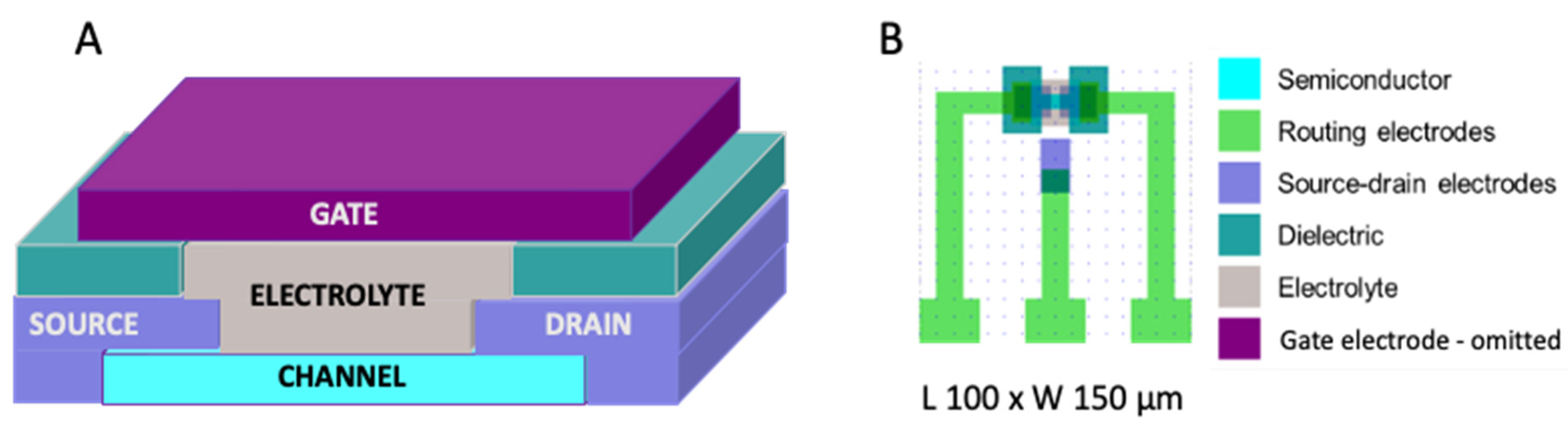
The OECT architecture used in the WEARPLEX project is presented in
Figure 1, depicting the device used in the addressing circuits. As in this case the switching time was more important than current throughput, an OECT channel width (W) and length (L) of 150 µm and 100 µm, respectively, were used.
In a WEARPLEX multi-pad electrode, each addressing circuit also has a number of driving OECT devices equal to the number of electrode pads. The requirement on these OECT devices is a high current throughput rather than a short switching time. Due to this, various channel geometries have been evaluated to optimize the devices toward multi-pad electrodes for stimulation applications. The current throughput scales with the W/L ratio, but the channel length is more or less limited by the resolution of the screen-printing equipment. However, the channel width is easily adjusted, and a larger width implies higher current levels in the ON state of the OECT. The correlation between the switching characteristics and the channel width of the OECT has briefly been reported previously by combining both experiments and simulations [
21]. In the work reported herein, driving OECT devices with channel widths of 1, 2, 3 and 6 mm were evaluated (see
Figure 2). The 6 mm wide channel obviously allowed the highest ON current level, but increasing the channel width also brought a trade-off with respect to the footprint. It should also be mentioned that an interdigitated design was used for the 6 mm wide channel (i.e., it was split into 6 parallel channels, each 1 mm wide). The use of an interdigitated design might be beneficial in other applications, but here it was considered disadvantageous since the leakage current was increased and the footprint of each device was enlarged. In order to not exceed the maximum dimensions of the multi-pad electrode, W = 1 mm was chosen for the drive OECTs in the circuits reported herein. This trade-off allowed for ON current levels up to a few mA, which at least exceeded the sensory threshold of the human body.
The transfer and output characteristics of the five different OECT architectures evaluated herein (L = 100 µm and W = (0.15, 1, 2, 3, 6) mm) are shown in
Figure 3.
The inks used in the OECTs and OECT-based circuits were screen-printed on plastic substrates based on polyethylene terephthalate (PET, Polifoil Bias, Policrom Screen, Carvico, Italy). PEDOT:PSS (Clevios S V4, Heraeus Epurio, Leverkusen, Germany) was used for the electrochemically active transistor channels and gate electrodes. The electrolyte (E003, developed by RISE, Norrköping, Sweden) was deposited by screen-printing, followed by UV-curing. Two different carbon inks (7102 and 7082, DuPont, Wilmington, DE, USA) were used for the source and drain contacts and printed resistors, respectively. A silver ink (Ag 5000, DuPont, Wilmington, DE, USA) was used for the printed interconnects, conductors and contact pads, while a dielectric ink (5018, DuPont, Wilmington, DE, USA) was used for insulation.
The materials of the standalone OECTs and OECT-based circuits were deposited by using flatbed sheet-fed screen-printing equipment (DEK Horizon 03iX) with screen meshes based on polyester threads. The OECT printing process developed by RISE is described in detail in [
19,
28], while the main steps are presented here for ease of understanding. Silver ink was printed as the first layer, providing the interconnects and contact pads. PEDOT:PSS was then screen-printed between the silver contact pads to form the transistor channel, followed by printing of the carbon-based source and drain electrodes. The separation between the source and drain electrodes defines the channel length, typically 100 µm in the devices reported herein. The channel width, defined by the width of the deposited PEDOT:PSS OECT channel material, was customized to 1, 2, 3 and 6 mm. The silver, the PEDOT:PSS and the carbon inks were all dried at 120 °C for 3 min. An insulating layer (5018) was then deposited and UV-cured to define the area of the subsequently deposited electrolyte layer. Yet another PEDOT:PSS layer was deposited onto the electrolyte patterns as the OECT gate electrodes. The logic circuits rely on the voltage division between the OECT and a screen-printed resistor ladder based on carbon ink 7082. Conductor crossings were created by the deposition of the insulating 5018 ink followed by the deposition of another layer of Ag 5000. The design layout for printing, containing almost 1000 OECTs split into both standalone OECTs and various kinds of logic circuits, covered approximately the area of an A4 sheet.
Additionally, we developed two testbeds for the purpose of characterization of various OECT architectures and functional testing and validation of the switching capability of integrated logic circuits based on the preferred OECT architectures.
2.2. Testbed for Characterization of Individual OECT Devices
The aim of the tests was to identify the functional operation range of the novel OECT circuit designs when implemented to control current propagation. The two primary parameters of interest were the output voltage and the output current, since the biphasic pulses were generated in the current-controlled high-voltage regime in electrical stimulation applications. This led to the design of a special testbed circuit built on the TY51822R3 mbed development platform (Switch Science, Shinjuku City, Japan) shown in the left part of
Figure 4. It included a custom-designed pulse generator circuit with voltage step up and a current feedback loop and allowed for manipulation of all stimulation parameters of interest through the firmware application: current amplitude (range: 0–10 mA, 100 µA step), pulse width (0–1000 µs, 1 µs step), stimulation frequency (1–100 Hz, 1 Hz step) and maximum output voltage (20–100 V, 1 V step). Note that the current and voltage levels targeted here were very high. Most other OECT applications described in the literature rely on lower current levels generated by a voltage typically ranging from several mV to a few volts. Hence, the requirement of the electrical stimulation application to deliver current levels in the mA range at a voltage supply of up to 100 V adds new challenges to the OECT technology. The means for adjusting the high and low voltage levels of the signals, which drive the gate electrodes of the OECTs in two parallel branches, were included to account for the variability present in the prototypes produced in this stage of development. Based on earlier observations with similar OECT architectures, there was a strive to achieve a narrow OECT input voltage window, since this prolongs the operational lifetimes of the devices [
29]. Hence, the low and high input voltage levels were set to 0.3 V and 1.3 V, respectively, thereby resulting in an OECT input voltage window of only 1 V.
The testbed included multiple points for connection of oscilloscope probes, which were selected to enable measurement and recording of the voltages and currents in the parallel branches needed for characterization of the printed OECTs. To facilitate the testing of different OECT architectures and samples, the testbed included two flexible flat cable (FFC) docks, as shown on the right side of
Figure 4.
The switching set-up, with the scheme presented in
Figure 5, leveraged a parallel configuration of two printed OECT devices, in which at least one device was open whenever a pulse was generated. This arrangement lowered the stress on each individual OECT device in switching and was in line with a realistic scenario (e.g., when the printed OECT circuit is part of a multi-pad electrode device). Activation of a specific OECT branch was performed through the voltage level adjustment circuit controlled directly by the testbed microcontroller (MCU). Each branch included a simplified human model equivalent circuit (HMEC) to allow measurement of the leakage current in the branch that should be closed. The model from the active branch (HMEC1 or HMEC2) together with the HMEC reference represented the output load equivalent to a human connected through two biomedical electrode pads. All the HMECs were equal, with a resistor in series with a capacitor and a resistor connected in parallel, as shown in the right panel of
Figure 5.
In current-controlled sources, such as the one used in the testbed, the output voltage is variable to account for the variability of the electrode skin contact and individual properties that result in different loads. A common approach in transcutaneous stimulation devices is to connect the external load between the high voltage and a point that floats to generate the targeted current [
30]. Thus, the stimuli generated between the electrode pair has a floating potential dependent on the attached load, which is different from the potential of the OECT controller and would cause significant drift over time. To overcome this, we introduced a Q1 MOSFET switch, which connected the drain terminal of the OECTs to the common ground when no pulse was generated. As the pulse durations in the applications of interest were typically short (<1 ms), the introduction of Q1 ensured that the OECTs were on the ground potential and thereby could be controlled via the voltages applied to gate terminals G1 and G2.
Four different OECT architectures were used in the experiments:
In each experiment, the OECT devices in the parallel branches were always of the same architecture, and the experiments were repeated with multiple samples of the same architecture. In all tests, one of the OECTs in the parallel branch was set to its conductive state by setting the gate voltage to the logic low level (~0.3 V), while the other OECT was set to its non-conductive state by setting the gate voltage to the logic high level (~1.3 V). The signals were recorded for 30 pulses, after which the respective states of these two transistors were reversed, and the recording was repeated. This process was performed for five different current amplitudes (1, 2, 5, 10 and 15 mA) as well as five different maximal output voltages of the pulse generator (20, 30, 40, 50 and 60 V). In addition, due to the inherent humidity dependence in electrolyte-gated transistors, the testing protocol considered changes in the humidity conditions by repeating the tests in two different relative humidity (RH) levels: 25 %RH and 65 %RH. The pulse width was 400 µs, and the stimulation frequency was set to 30 Hz in all tests, which were parameter values corresponding to the standard protocol in the applications of interest.
2.3. Testbed for Validation of OECT-Based Demultiplexer Switching Capabilities
For validation of the printed OECT-based demultiplexer circuits, we designed a testbed featuring a single-channel current-controlled stimulator and a custom digital output board for control of the printed 2–4 OECT-based demultiplexer circuits that allowed routing of the stimulation signal to an arbitrary pad of a multi-pad electrode (see
Figure 6). The digital output board contained integrated adjustable voltage dividers that converted the signals from the digital logic outputs of the MCU to OECT driving voltages, here set to 1.3 V for logic high and 0.3 V for logic low. The testbed was based on the same modular architecture used for the OECT characterization, allowing them to share the same MCU and pulse generator modules. The firmware was upgraded to include control of the board for the digital outputs and a communication module for real-time selection of the active pad through a wireless channel.
The validation process included sequential pad activation by shifting the output state of the printed OECT-based logic circuits. All four output currents were measured in all states. The measurements in this test were performed with the pulse generator set at a maximal output voltage of 20 V and a current amplitude of 2 mA, conditions in which optimal performance was observed during the characterizations of the standalone OECTs. With this, the effects of the inherent variability in the switching characteristics of the OECTs in each of the four branches of the decoders, as well as the cumulative error caused by the cascade connection of 6 OECTs in the printed 2–4 demultiplexer unit, were minimized. The pulse width and the stimulation frequency were kept at 400 µs and 30 Hz, respectively.
3. Results
In the first test, the aim was to analyse the performance of various OECT architectures designed for high current throughput. The results of the comprehensive tests, including various levels of current amplitudes and pulse generator maximal voltages, are summarized in several representative figures.
Figure 7 shows the current measured in both parallel branches when one OECT was switched off (left panel) and the other OECT was in its conductive on state (right panel). Here, the results based on a maximal output voltage of 40 V and a current amplitude of 5 mA are depicted, since these were the output parameters most representative of real stimulation scenarios. It can be noted from the graphs that the 6 × 1 mm transistor architecture showed the worst performance, with the leakage current in the closed branch comparable to the current measured in the conducting branch. The OECT with a 3 mm channel width also showed subpar performance, with a current leakage above 1 mA, or 20% of the current level in the conducting state. The OECTs with 1 mm and 2 mm channel widths showed comparable performance, with an average leakage current below 0.5 mA for both designs.
Further analysis of the current leakage in the closed branch was performed for various levels of stimulation amplitudes in two scenarios: with the maximal output voltage of the pulse generator at 30 V (
Figure 8, left panel) and 40 V (
Figure 8, right panel). An estimation of the bounds of the expected current leakage was performed based on measurements in both possible states of the parallel branches. (One OECT was conductive, while the other was non-conductive, and vice versa.) It can be noted that for both cases, the current leakage was higher for low amplitudes (1 mA and 2 mA), while the leakage stabilized for currents above 5 mA. At 30 V, the output leakage was around 5% for the 1 mm, 2 mm and 3 mm OECT channel widths, while it was close to 15% for the 6 × 1 mm OECT architecture. At 40 V, the output leakage was more pronounced for all architectures. Additionally, the system stability was compromised, which can be noted from the high variability of the measured leakage current when comparing one state (branch 1 open, branch 2 closed) with the other state (branch 1 closed, branch 2 open), as reflected by the estimated bounds of the expected current leakage.
Figure 9 shows the measured current levels for various maximal output voltages of the pulse generator. Here, the results are shown for the OECT architecture with a 1 mm channel width and the stimulation current of 5 mA, with the measurements of the nonconductive branch in the left panel and the conductive branch in the right panel. It can be noted that that there was a negative relation between the maximal output voltage and the leakage current. However, for voltage levels of 40 V or below, the current leakage was relatively low (<0.5 mA), meaning that over 90% of the current was flowing through the conductive branch. Conversely, for 50 V and above, the current in the closed branch was comparable to the current in the open branch, with approximately 2.5 mA running through both branches.
When analysing the right panel, it can also be noted that for a low maximal output voltage, the required current could not be generated throughout the pulse. In the negative phase, this was evident even for the 40 V maximal output voltage and even more pronounced for lower values, especially for the 20 V level.
The measurements obtained when comparing the performance of devices with a 1 mm channel width in 25 and 65 %RH conditions are shown in
Figure 10. Here, the measured currents in the non-conductive (left) and conductive (right) branches were obtained while a 40 V maximal output voltage and current levels of either 5 mA or 10 mA were provided by the generator set-up. The results indicated a current leakage of less than 0.5 mA for both input currents at 65 %RH conditions, while the current leakage was close to one half of the input current at 25 %RH.
The results from the experiment with the screen-printed OECT-based 2–4 demultiplexer circuits for control of the stimulation current in multi-pad electrodes are shown in
Figure 11. The currents measured in each of the four output nodes of the demultiplexer circuit are shown in a testing sequence where the conductive branch was changed every 2 s, with the stimulation pulse from the pulse generator set at 2 mA at a 20 V maximal output voltage. It can be noted that there was a slight variability of the output signals of the printed logic circuit and some expected leakage in the closed channels. However, in all experiments, the conductive branch of the demultiplexing unit was selected correctly and at the appropriate time. In addition, the current in that branch was significantly higher than in all other branches, and at the same time, it almost reached the targeted level of 2 mA.
4. Discussion
The results confirmed that printed OECT devices can be used for the routing of current-controlled pulses in the voltage and current ranges used in a number of transcutaneous electrical stimulation applications. Despite the clear limitations in the voltage levels and the current throughput of the tested OECT architectures, the results indicate that the proposed concept of electrode arrays with integrated logic circuits indeed provides great potential for the next generation of multi-pad electrodes. The working range of the tested architectures can already be recognized as sufficient in the domain of several applications of interest, like iontophoresis, proliferation, regenerative applications and electrotactile stimulation.
In electrotactile applications, current amplitudes of up to 10 mA at maximal output voltages below 40 V could be considered to be at the limit of the more general requirements, but for specific electrode sizes and placements at these levels, they could be considered sufficient to produce clear tactile feedback [
15]. For TENS and Functional Electrical Stimulation (FES) applications [
3,
7,
8,
17,
30], which require higher voltages and currents, the design of the OECT architectures can be adopted to reduce the demand from a single output transistor. This can be achieved by stimulation configurations and protocols in which multiple branches are conductive at the same time (i.e., by smart electrodes with integrated shift register circuitry designed to activate several pads on the multi-pad electrode at the same time), thus reducing the demand on the single-output transistor. This limits the flexibility and imposes slight limitations in terms of possible electrode designs (i.e., pad size and arrangement) but can cover many application scenarios of interest in which the targeted activation points are not densely distributed.
The experiments conducted in this study have shown that none of the devices tested were able to completely switch off the current passing through the non-conductive branch of the testbed. As can be seen in
Figure 7 and
Figure 8, in each architecture, there was a small leakage current through the non-conductive branch. Both the 1 mm and the 2 mm OECT channel width the architectures showed similar, satisfactory performance in the tested conditions. The 3 mm OECT channel width architecture showed significantly higher leakage currents, indicating that there might be a (non-linear) relation between the channel size and the leakage current. Furthermore, this property seemed to be cumulative, as can be observed when comparing the 1 mm and the interdigitated 6 × 1 mm OECT channel width architectures. The latter architecture was designed to increase the maximal current throughput capacity of the device by leveraging the principle of current distribution through parallel structures. However, the same principle seems to apply to the leakage currents, which in the tested conditions reached approximately 50% of the 5-mA output current, meaning that in the application of interest the device acted more or less as a short-circuit in both states. In all other architectures tested, the current that passed through the non-conductive branch could be considered negligible for the application of interest, as current levels below 1 mA, generated by voltages below 40 V, were unable to produce action potentials in the subcutaneous structures with the pulses used, since these values were below the thresholds defined by the strength–duration curves for peripheral nerves [
31]. The 40 V value seemed to be near the maximal voltage of the operating range, as some of the 2 mm and 3 mm OECT channel widths maintained the switching capacity by exhibiting a leakage current below 1 mA, while other devices failed to cut off the current when acting as a parallel open branch, as evidenced by the 50% current throughout being allowed.
The use of current-controlled biphasic pulses is common practice in electrical stimulation. The pulse in the second phase—the compensation phase—extracted the charge introduced in the activation phase, thus preventing local charge build-up that can lead to reduced stimulation effectiveness or even tissue damage. The same principle is beneficial for the use of printed OECT switches. PEDOT:PSS-based OECTs are operated in the third quadrant (i.e., a negative drain voltage is required to reach a state in which the OECT channel is completely switched off). On the contrary, a positive drain voltage turned the OECT device toward a diode-switching behavior. However, switching the polarity of the biphasic pulse during stimulation increased the efficacy, as well as the expected operational lifetime, to a large extent due to the fact that the pulse length of the respective pulse was in the sub-ms range. It should be noted though that the shape of the recorded current during the stimulation was not ideally symmetrical in the two phases. This peculiarity may be caused by the behavior inherent to the electrical stimulation current control circuitry. The external load, which is an analog to a simplified model of the human skin, had both resistive and capacitive elements that acted as an RC filter to the current source. Here, the current amplitudes of the pulses were controlled by changing (increasing) the output voltage to maintain the desired level. Once the maximal output voltage was reached, the current dropped while the capacitor was charging. This can be seen in the shape of the first pulse. However, in the second pulse phase, the current drop was delayed, as the capacitor was already fully charged by the opposite polarity, acting as a voltage buffer. Since a symmetrical pulse is desired, this effect can be compensated for by tuning the current control algorithm after the OECT circuit has been characterized. This poses an interesting challenge for future research and development activities in this domain.
Additionally, a presence of ripples can be noted in the signals recorded with the first testbed, which are shown in
Figure 7,
Figure 9 and
Figure 10. These were caused by the implemented current-controlled system, which was not optimized for the additional dynamics introduced by the OECT circuit and the specific HMEC, resulting in minor overshoots of the setpoint. Conversely, in the second testbed, the output module was specifically designed to be used with the OECT-based smart electrodes with a 2–4 decoder. As can be noted in
Figure 11, the ripples in the signals were significantly lower and were on a level comparable to the measurement noise. These could be further suppressed by additional system tuning, but they were already inconsequential to the targeted application at the presented level.
Due to the current-controlled method that increases the voltage until the desired current level is reached, the maximal voltage level is a critical parameter that will dictate the performance of the OECTs and hence also the current leakage in the closed branches. The graphs shown in
Figure 9 demonstrate that for voltage levels of 50 V and above, the OECT devices were not able to control the current propagation, as the current in the closed branch was comparable to the current in the open branch (approximately 2.5 mA). For voltages of 40 V and below, the current was propagating primarily through the branch with the OECT in the open state, with leakage currents of approximately 0.5 mA in the branch with the OECT in the closed state. It should be noted that these results were analyzed for OECT devices with a 1 mm channel width, since they showed comparable performance with the 2 mm channel width devices and better performance compared with other architectures for the testing scenario at 40 V. From the current signals shown in the right panel, it can be noted that due to the high capacitance of the HMEC, the required 5-mA current level was not generated, nor did it reach the steady state throughout the pulse for some of the voltage output levels. This was evident for the 40 V maximal output voltage but became gradually even more pronounced for the lowered voltage levels of 30 V and 20 V. This illustrates the need for a high output voltage in applications relying on transcutaneous electrodes with pads of relatively small contact areas between the electrode and the skin, requiring current levels exceeding 3–4 mA.
Another factor that will affect the current leakage is the output current. This effect is noticeable in the current leakage vs. total current graphs shown in
Figure 8. With a 30 V output voltage, the current leakage was considerable (>10% for all OECT architectures) for low currents (1 and 2 mA), but the current leakage was reduced and stabilized when the current was further increased (around 5% for the 1 mm, 2 mm and 3 mm OECT architectures and around 13% for 6 × 1 mm OECT architecture). A similar behavior was observed when the maximal voltage was set to 40 V, but in this case, the transistor performance was significantly degraded (consistent 50% current leakage for the 6 × 1 mm architecture and 20–30% leakage for the other architectures). Furthermore, there was a notable inter-device variability reflected through the wide ranges of the recorded leakage currents. This was potentially a result of variations originating from the manufacturing process (e.g., ink homogeneity, non-uniform curing process, thickness variations and moisture level fluctuations in the channel).
Humidity is clearly another factor that influences the performance of printed OECT-based circuits, and our results demonstrated this effect for the current-controlled electrical stimulation pulses. The testing was performed in humidity conditions just outside the range recommended by most professional bodies but still within the range required by the majority of the regulatory bodies [
32]. From
Figure 10, by directly comparing the dashed lines with the solid lines, it can be observed that for the same set of OECTs, the leakage current in the closed branch was minimized in high-humidity conditions. For a maximal output voltage of 40 V, there were two current levels at which the OECTs were unable to function (i.e., current dissipation close to 50%) at 25 %RH, but the increase in the relative humidity to 65 %RH resulted in a reduction of the current leakage to the level of 5%. It should be noted that the electrodes for transcutaneous electrical stimulation were located on the skin, which usually implies a moist microenvironment [
33,
34]. Hence, improved OECT operation in high-RH conditions is desirable with respect to the application scenario, and one solution to mitigate the RH dependence is to combine the OECT screen-printing process with an appropriate encapsulation process. The advantage of properly encapsulated OECT-based circuits is that an identical drive protocol can be used throughout a wider RH range, which in turn results in a prolonged operational lifetime.
The final demonstration of the performance of an OECT-based screen-printed demultiplexer circuit (shown in
Figure 8) further evidences that this technology can serve as a basis for smart biomedical electrodes that integrate logic circuits to allow for direct pad addressing. Considering that the 2–4 demultiplexer circuit integrates 16 printed OECTs, and by also taking into account the potential influence of inter-device variability within the circuit, the stimulation requirements were reduced compared with the previous tests done with the standalone OECTs (i.e., the maximal voltage was set to 20 V and the input current level to 2 mA). From the currents in the four output channels of the demultiplexer, it can be concluded that the current in the active channel was very close to the desired output current level and that the leakage currents in the remaining three output channels were minimal. The variability of the printed OECTs will, to some extent, influence the outputs, since the respective channel will exhibit a different current throughput as well as leakage current level, but from a demonstration perspective, the evaluated circuits are considered functional.
There are problems that need to be addressed in future research and development activities. We foresee that a change in the OECT architecture that will allow for increased voltage and current levels will be required by many applications. Furthermore, we aim to address the OECT variability by advancements in the production process but also by ensuring switching performance robust to humidity fluctuations through the development of a stable skin interface that maintains the moistness of the skin electrode contact, thus ensuring a humid environment. However, the results presented here provide evidence that we are on the verge of reaching the next generation of printed multi-pad biomedical electrodes with embedded logic circuits based on printed OECTs.


 ,
, 