
An Integrated Photorefractive Analog Matrix-Vector Multiplier for Machine Learning †

 , , , and
Abstract
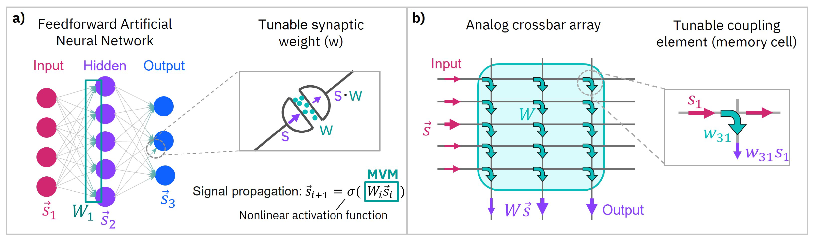
:1. Introduction
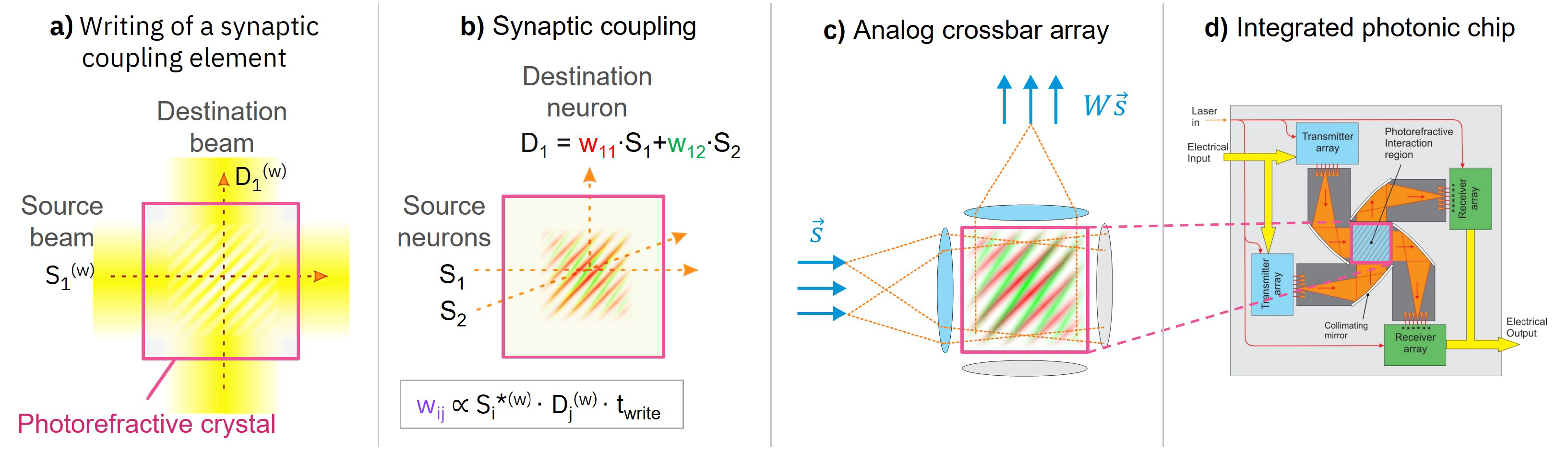
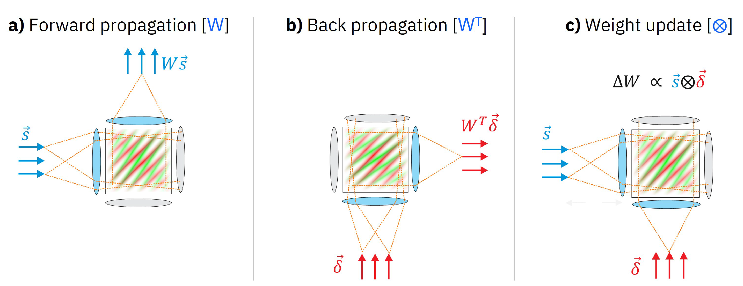
2. Materials and Methods
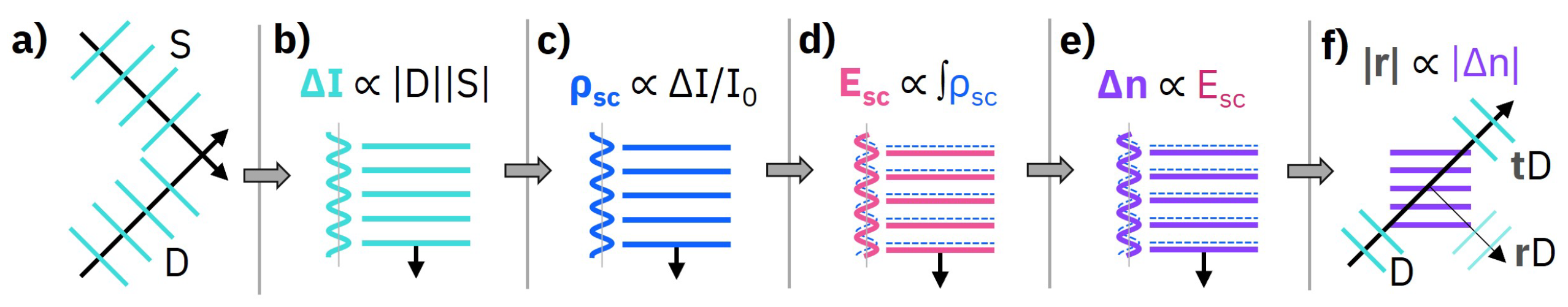
2.1. Photorefractive Effect
2.1.1. Background
2.1.2. Crossbar Array Architecture
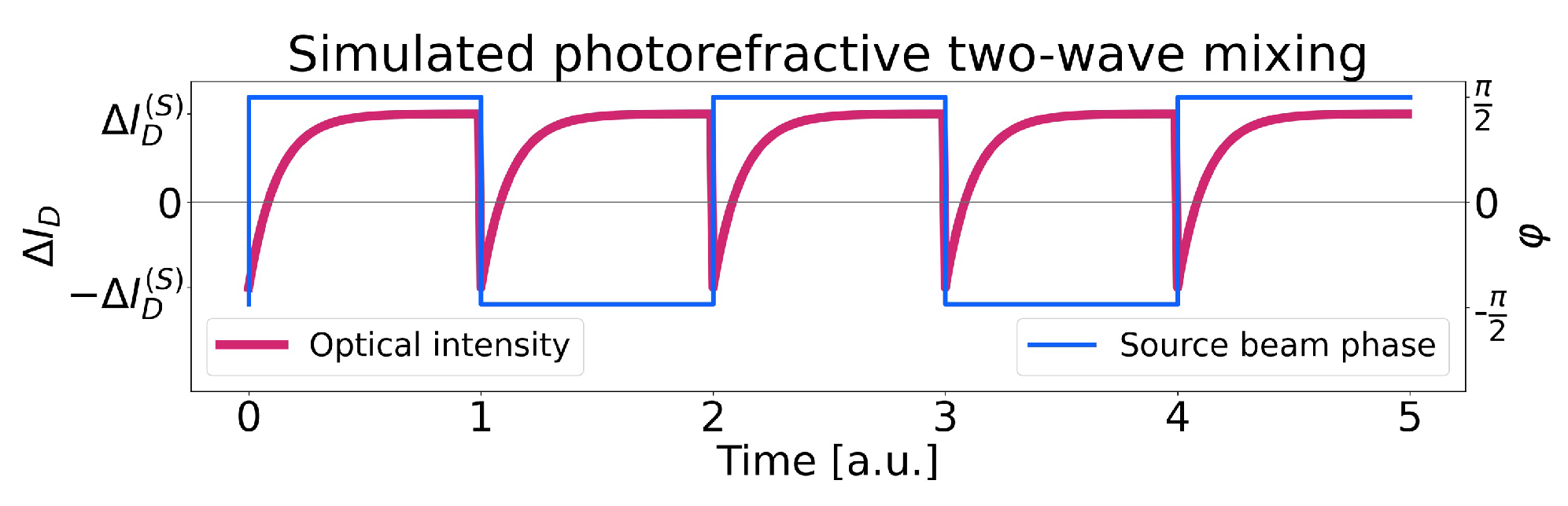
2.1.3. Two-Wave Mixing
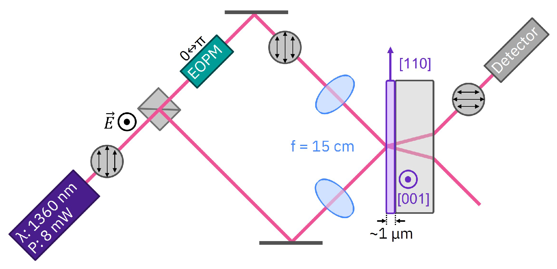
2.1.4. Experimental Setup for Two-Wave Mixing
2.1.5. Photonic Prototype Chip Design
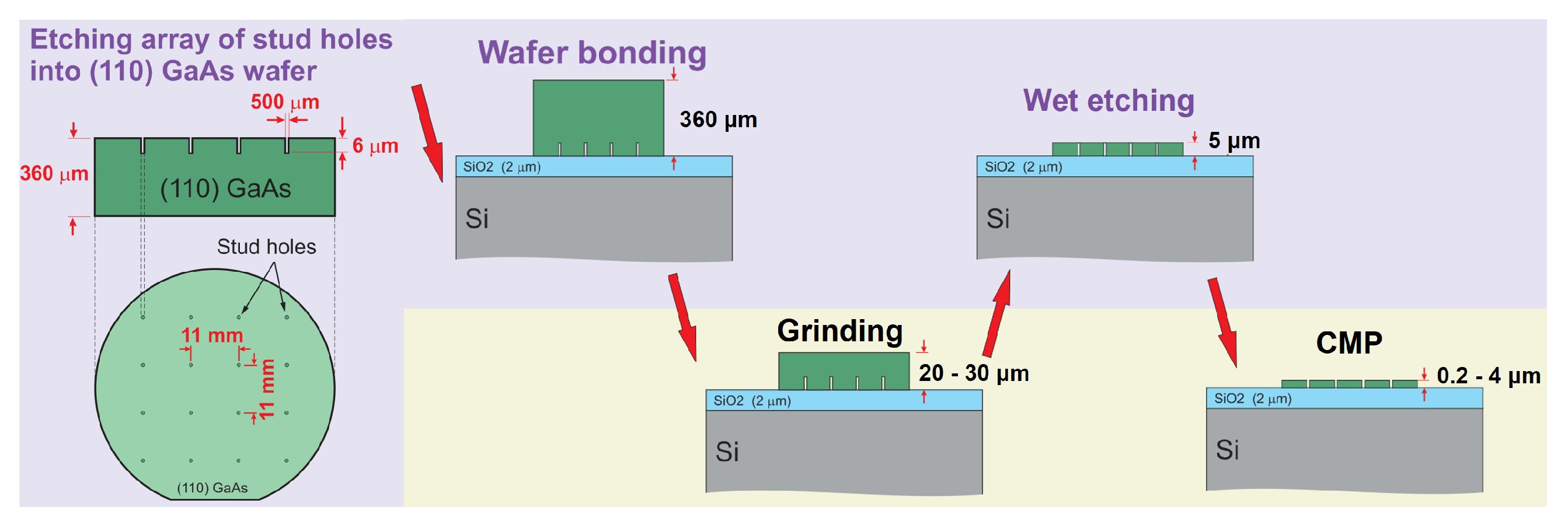
2.2. Fabrication
2.3. Integrated Photonic Measurement Setup
3. Results
3.1. Characterization of the GaAs-Based Integrated Photonic Platform
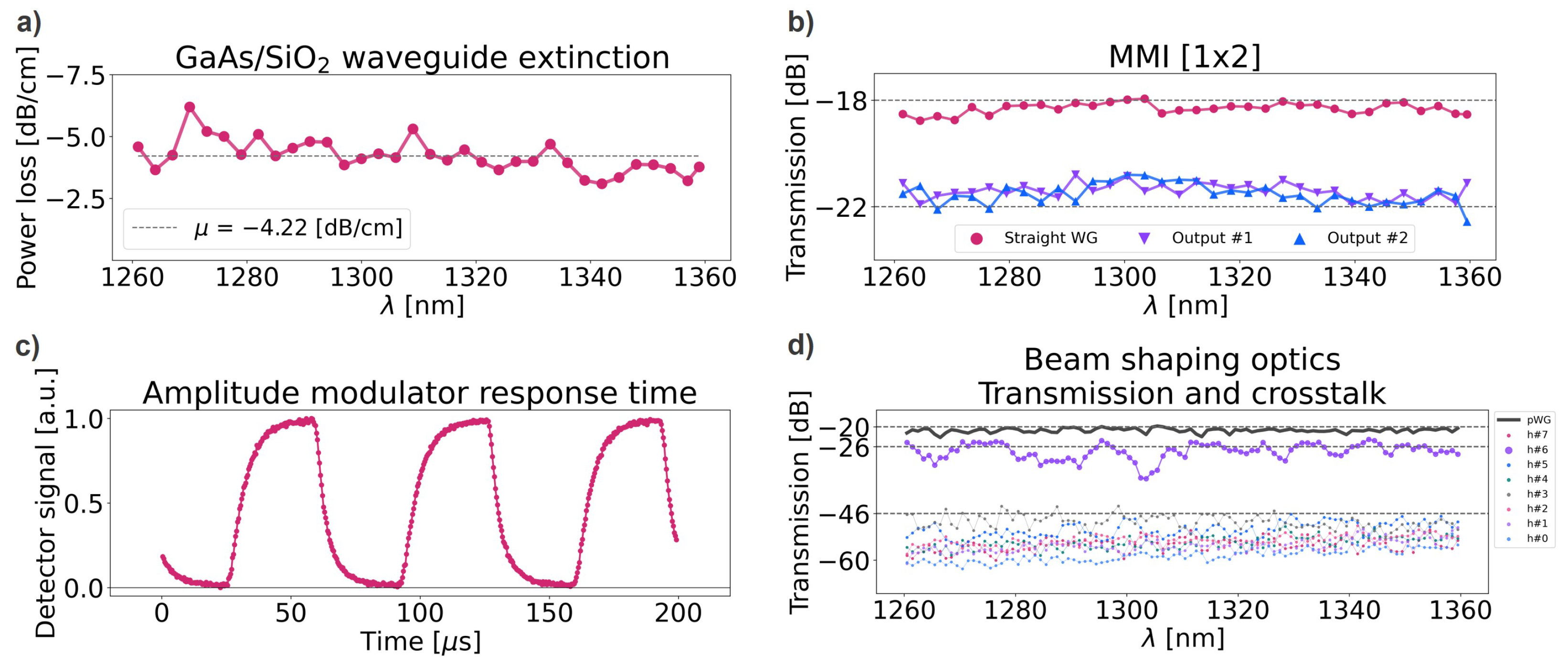
- Figure 10a: The GaAs/SiO waveguides display a typical propagation loss of less than 5 dB/cm. The extinction coefficient was obtained by comparing the transmission through different lengths of waveguide.
- Figure 10b: 1 × 2 MMIs display the correct approximate −3 dB attenuation compared to a reference waveguide.
- Figure 10d: This graph displays the power transmission through the photorefractive processor (Figure 8a). The experiment was performed by inserting light via a single input channel. Specifically, the input was not split up by an MMI into both input branches as denoted in Figure 8a. The black line corresponds to a waveguide that follows a similar trajectory as the light inside the processor and acts as a reference. The thick purple line denotes the signal from the designated output channel, whereas the thin lines denote the output from the neighboring output channels.The input channel is correctly transmitted to the designated output channel. The key performance indicators are the contrast between the designated output channel and its neighbors and the attenuation compared to reference. Both are indicative of the correct collimation and refocusing of the input beam and the undistorted propagation through the GaAs slab waveguide. The contrast between the target output channel and its neighboring output channels is retrieved at around 20 dB. The transmission through the processor yields less than −6 dB power attenuation at wavelength bands along the entire spectral range.
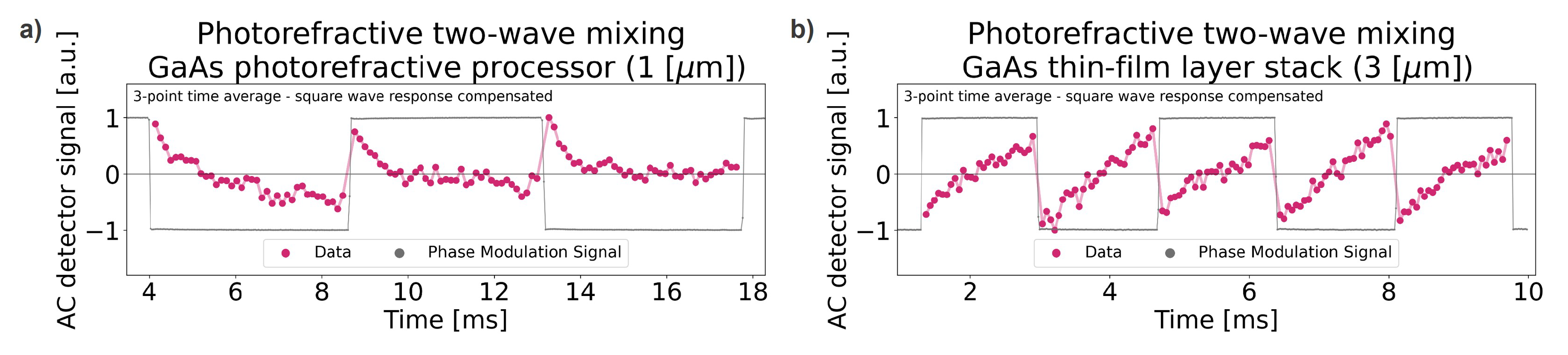
3.2. Photorefractive Characterization of Thin-Film GaAs Layers
4. Discussion
5. Conclusions
Author Contributions
Funding
Data Availability Statement
Acknowledgments
Conflicts of Interest
References
- Bommasani, R.; Hudson, D.A.; Adeli, E.; Altman, R.; Arora, S.; Arx, S.V.; Bernstein, M.S.; Bohg, J.; Bosselut, A.; Brunskill, E.; et al. On the Opportunities and Risks of Foundation Models. arXiv 2021, arXiv:2108.07258. [Google Scholar]
- Strubell, E.; Ganesh, A.; McCallum, A. Energy and policy considerations for modern deep learning research. In Proceedings of the AAAI 2020—34th AAAI Conference on Artificial Intelligence, New York, NY, USA, 7–12 February 2020; pp. 13693–13696. [Google Scholar] [CrossRef]
- Amodei, D.; Danny, H. AI and Compute. 2018. Available online: https://openai.com/blog/ai-and-compute/ (accessed on 18 April 2022).
- Stark, P.; Horst, F.; Dangel, R.; Weiss, J.; Offrein, B.J. Opportunities for integrated photonic neural networks. Nanophotonics 2020, 9, 4221–4232. [Google Scholar] [CrossRef]
- Sebastian, A.; Le Gallo, M.; Khaddam-Aljameh, R.; Eleftheriou, E. Memory devices and applications for in-memory computing. Nat. Nanotechnol. 2020, 15, 529–544. [Google Scholar] [CrossRef] [PubMed]
- Burr, G.W.; Shelby, R.M.; Sebastian, A.; Kim, S.; Kim, S.; Sidler, S.; Virwani, K.; Ishii, M.; Narayanan, P.; Fumarola, A.; et al. Neuromorphic computing using non-volatile memory. Adv. Phys. X 2017, 2, 89–124. [Google Scholar] [CrossRef]
- Han, S.; Liu, X.; Mao, H.; Pu, J.; Pedram, A.; Horowitz, M.A.; Dally, W.J. EIE: Efficient Inference Engine on Compressed Deep Neural Network. In Proceedings of the 2016 43rd International Symposium on Computer Architecture, ISCA, Seoul, South Korea, 18–22 June 2016; Volume 16, pp. 243–254. [Google Scholar] [CrossRef] [Green Version]
- Rumelhart, D.; Hinton, G.; Williams, R. Learning representations by back-propagating errors. Nature 1986, 323, 533–536. [Google Scholar] [CrossRef]
- Kriegeskorte, N.; Golan, T. Neural network models and deep learning. Curr. Biol. 2019, 29, R231–R236. [Google Scholar] [CrossRef] [PubMed]
- Cronin-golomb, M.; Klein, M. Photorefractive Materials and Devices. In Handbook of Optics: Devices, Measurements, and Properties, 2nd ed.; McGraw-Hill: New York, NY, USA, 1995; Volume 2, Chapter 39; pp. 1–42. [Google Scholar]
- Owechko, Y.; Soffer, B.H. Holographic Neurocomputer Utilizing Laser Diode Light Source. SPIE 1995, 2565, 12–19. [Google Scholar]
- Yeh, P. Two-Wave Mixing in Nonlinear Media. IEEE J. Quantum Electron. 1989, 25, 484–519. [Google Scholar] [CrossRef]


| Trace #1 | Trace #2 | Trace #3 | Average | |
|---|---|---|---|---|
| Heating | 4.3 | 4.3 | - | 4.3 ± 0.1 |
| Cooling | 6.0 | 6.1 | 5.9 | 6.0 ± 0.1 |
Publisher’s Note: MDPI stays neutral with regard to jurisdictional claims in published maps and institutional affiliations. |
© 2022 by the authors. Licensee MDPI, Basel, Switzerland. This article is an open access article distributed under the terms and conditions of the Creative Commons Attribution (CC BY) license (https://creativecommons.org/licenses/by/4.0/).
Share and Cite
Vlieg, E.A.; Talandier, L.; Dangel, R.; Horst, F.; Offrein, B.J. An Integrated Photorefractive Analog Matrix-Vector Multiplier for Machine Learning. Appl. Sci. 2022, 12, 4226. https://doi.org/10.3390/app12094226
Vlieg EA, Talandier L, Dangel R, Horst F, Offrein BJ. An Integrated Photorefractive Analog Matrix-Vector Multiplier for Machine Learning. Applied Sciences. 2022; 12(9):4226. https://doi.org/10.3390/app12094226
Chicago/Turabian StyleVlieg, Elger A., Lucas Talandier, Roger Dangel, Folkert Horst, and Bert J. Offrein. 2022. "An Integrated Photorefractive Analog Matrix-Vector Multiplier for Machine Learning" Applied Sciences 12, no. 9: 4226. https://doi.org/10.3390/app12094226