Review

Modulation Characteristics of High-Speed Transistor Lasers

1
State Key Laboratory of Luminescence and Application, Changchun Institute of Optics, Fine Mechanics and Physics, Chinese Academy of Sciences, Changchun 130033, China
2
Daheng College, University of Chinese Academy of Sciences, Beijing 100049, China
3
Jlight Semiconductor Technology Co., Ltd., Changchun 130102, China
*
Authors to whom correspondence should be addressed.
Appl. Sci. 2022, 12(9), 4475; https://doi.org/10.3390/app12094475
Submission received: 28 January 2022 / Revised: 10 March 2022 / Accepted: 15 March 2022 / Published: 28 April 2022

Abstract

:
The spontaneous emission recombination lifetime of carriers in the active region of transistor lasers (TLs) is significantly reduced due to the accelerated carrier transport in the base region under the collector bias. Thus, it has the potential for use as a high-speed optical fiber communication light source. The unique three-electrode structure of TL notably enriches the modulation methods of the light source. As an important parameter to measure the data transfer rate, the modulation bandwidth of TL has been studied extensively. This paper briefly analyzes the inherent characteristics and advantages of TL and then discusses the progress in the research on TL modulation characteristics. Currently, the common methods to increase the modulation rate include optimizing the device structure, intracavity photon-assisted tunneling, and adding external auxiliary circuits. Through these techniques, single quantum well GaAs- based TL can achieve error-free transmission of 22 Gb/s, and simulation data show that for InP- based TL, this can reach 40 Gb/s. Finally, the challenges faced by TL in the area of optical fiber communication are elucidated.

1. Introduction

Since the creation of transistors and lasers, numerous scientists have attempted to combine the electrical signals of transistors with the optical signals of lasers [1,2,3,4]. The transistor laser (TL) was the first electro-optical hybrid device that could output an optical signal and an electrical signal [5].
In contrast to industrial semiconductor lasers (such as those for additive manufacturing [6], laser-foil-printing [7], and laser melting [8,9,10]), where the focus is on the electro-optical conversion efficiency, output power, and reliability, the primary focus for TL is modulation rate performance, with the goal of becoming the core light source device for next-generation high-speed communication systems.
The carrier lifetime of TL in the active region is as low as 30–40 ps [11]. This significant advantage has extraordinary application potential in the fields of fast optical logic gates [12] and fast modulation [1]. In the field of semiconductor lasers applied to fiber transmission (mainly in the 1310 nm and 1550 nm bands), conventional directly modulated lasers (DMLs) suffer from long carrier recombination lifetimes (approximately 1 ns) [13] and serious carrier accumulation; thus, the transmission rate of DML is limited to less than 50 Gb/s [14]. It is difficult to overcome this limitation without the use of four-level pulse amplitude modulation [15] or hetero-integrated structures such as substrate lift-off and die bonding [16]. TL has the inherent advantage of short carrier lifetime, and the unique three-electrode structure increases the choice of modulation methods. Therefore, TL is expected to replace DML in optical fiber communication.
However, compared with DML, substantially less research has been conducted on TL. More research is needed on TL to address various issues. Among these is the fact that the power of TL is less than the commercially required level, which also limits its modulation capability (see Section 2.2). Further, numerous problems relating to long-wavelength InP- based TL need to be addressed before it is commercially used in optical fiber communication; these problems include low mode gain [17] and strong inter-valence band absorption in the base region [18]. Although these shortcomings limit the application of TL, it has been reported that the modulation characteristics (including bandwidth, power, and transmission rate) of TL can be improved by optimizing the base structures (e.g., quantum well (QW)) and introducing intracavity photon-assisted tunneling and external auxiliary circuits. This paper introduces and discusses methods that can improve the modulation performance of TL based on the abovementioned schemes.

2. Inherent Advantages of TL

In 2004, Feng et al. introduced TL as a new type of heterojunction bipolar transistor laser [19]. The energy band structure of the device is shown in Figure 1. By introducing a QW active region and a Fabry–Perot resonant cavity into the base region of an electrical transistor, electrical and optical gains can be obtained [20,21]. For an input base current, the optical signal of the active region and the electrical signal of the collector can be obtained simultaneously, which provides a new direction for photoelectronic integration.

2.1. Independent Control of Output Wavelength and Power

For comparison, the structure diagrams of DML and TL are shown in Figure 2. For DML, changing the voltage changes the output power of the device because it changes the number of carriers injected into the active region. Further, changing the voltage also changes the output wavelength because it changes the band structure of the QW. In contrast, for TL, the amount of carrier injection in the active region is mainly controlled by the base-emitter voltage VBE, while the energy band structure is mainly controlled by the base-collector voltage VBC. Therefore, while changing the output power of the TL, the energy band structure is not significantly affected and the dispersion of the output wavelength as the power changes is reduced. It thus follows that the modulation ability of TL is better than that of DML [22].

2.2. Drastically Reduced Effective Carrier Recombination Lifetime

Figure 3a,b show the energy band structure and carrier density distribution of double-heterojunction DML and TL [23]. For DML, due to the double- heterojunction structure, a large number of electrons injected from the N region cannot reach the P region within the recombination time. Consequently, they accumulate in the active region and increase the recombination lifetime. Meanwhile, the injected holes also accumulate in the valence band. This situation results in a uniform distribution of carriers, which induces relaxation oscillations and transport delays. For TL, because of the base transition in the transistor, the carriers that are not recombined within the base transition time are collected by the collector. Therefore, the recombination lifetime of TL is not higher than the transit time of the base region, and the long-lived carriers leave the active region in time to greatly alleviate the carrier accumulation of TL. The carrier distribution of NPN-type TL can be simply drawn if the charge at the boundary between the collector and base is assumed to be zero, which is shown in Figure 3b. Note that although this unique slanted distribution defines the fast characteristics of TL, it is evident that the number of carriers involved in recombination to emit photons is much less than that of DML. However, for a device applied to high-speed modulation, high power is the goal that needs to be pursued because it means longer transmission distance and higher modulation bandwidth. Achieving this is the main challenge for TL.
Assuming that the amount of recombination in the active region is much greater than that in other regions of the base region, the charge distribution of the base can be approximated as a superposition of two triangular charge groups represented by Q1 and Q2 [24,25]. Q 1   =   q Δ n 1 A W E Q W / 2 represents the carrier transported from the emitter to the QW, and Q 2   =   q Δ n 2 A W E C / 2 represents the carrier transported from the emitter to the collector. Δ n 1 and Δ n 2 are the electron concentrations to the QW and collector, and the integral values for Δ n 1 and Δ n 2 along the electron transfer direction are Q1 and Q2, respectively. WEQW is the distance from the emitter to the QW and WEC is the distance from the emitter to the collector. The carrier model of TL was reported by Taghavi et al. [26], which is simplified in Figure 4b. Assuming that the carriers passing through the left separation confinement heterostructure (SCH) layer are trapped by the first QW and the remaining carriers continue to diffuse through the barrier to the next well until they are trapped by other wells, the carrier transport model in the base region can be established when hot-electron escape and QW tunneling are considered. It can be seen in Figure 4a that the carrier density gradually decreases from the E region to the C region, and the amount of reduction also decreases, which indicates that the QW closer to the C region has a weaker capture ability for electrons. In Figure 4b, τsch2 is the lifetime of carriers passing through the base region from the left SCH layer to the right SCH layer, τsch1 is the diffusion time of carriers from the left SCH layer, τcap1 is the QW1 trapping lifetime, τbar is the diffusion time between QWs, τqw1 is the effective radiative recombination of carriers in the QW1 region lifetime, including spontaneous emission and stimulated emission within the QW, τsch is the spontaneous emission recombination lifetime of carriers in the SCH layer, τtun is the tunneling carrier time between wells, τtherm is the hot-electron escape time, WB is the base width, Lb is the barrier width, WQW is the quantum well thickness, and WSCH1 and WSCH2 are the upper and lower base, respectively, of the SCH layer thicknesses. The green line in Figure 4b is the forward route of the carriers in the base region; most of the carriers participate in the transition from the base region, and the rest enter the QW to participate in the recombination. The carriers entering the QW generate photons through radiative transition, and some of them escape through hot electrons or tunnel electrons into other QWs.
The frequency response H(ω) of TL is expressed as
H ω = A 0 1 ω 2 ω n 2 + j 2 ω / ω n ξ ,
where ωn, the relaxation oscillation damping factor ξ, relaxation frequency fR, and the relaxation peak amplitude H(ωR) are defined as follows:
ω n 2 = Γ ν g N ph τ ph = η I B / I TH 1 τ ph τ B , spon ,
ξ = 1 2 ω n τ B , spon + τ ph ω n 2 ,
f R = ω n 2 π 1 2 ξ 2 ,
H ω R 2 = A 0 2 4 1 ξ 2 ξ 2 .
The modulation bandwidth ω3dB denotes the response frequency when H(ωR) = −3 dB. The parameters involved in the formulas include normalization factor A0, optical confinement factor Γ, group velocity ν, differential gain g’, spontaneous emission recombination lifetime τB,spon, photon lifetime τph, photon number Nph, and slope efficiency η.
Although DML is the most commonly used light source for optical communication, its modulation capability is inherently limited by relaxation oscillation [27]. The relaxation oscillation deteriorates the modulation characteristics mainly by reducing the bandwidth ω3dB and increasing the relaxation peak H(ωR). The shorter carrier lifetime of TL [13] can improve the relaxation oscillation damping factor ξ, thus increasing ωn and modulation bandwidth ω3dB while effectively reducing the relaxation oscillation resonance peak H(ωR) [23]. The increase in H(ωR) is the main reason for distortion during optical signal transmission. Xu et al. used a 40 Gb/s NRZ pseudorandom bit sequence with a word length of 27-1 to simulate eye diagrams of DML and TL. The eye diagram of TL is wider because the rise and fall times of the digital signal transmission of the TL are shorter than that of the DML, which means that the signal transmitted by the DML is more prone to distortion [28]. A low H(ωR) of TL means that the area available for signal transmission is widened, and the actual signal transmission rate is increased. Although the bandwidth of the GaAs -based TL reported by Tan et al. was approximately 17 GHz, the data transfer rate reached 40 Gb/s. Therefore, the ratio of transmission rate to bandwidth is as high as 2.35, which is significantly higher than the 1.25 ratio of DML [13].

3. Modulation Characteristics of TL

In current research on TL modulation and data transmission characteristics, approaches such as optimization of QW, optimization of the base region, introduction of intra-cavity photon-assisted tunneling, and introduction of external circuit assistance have been proposed. These approaches reduce the carrier recombination lifetime or photon lifetime; further, they can increase the photon density or increase the rate of change of the output optical power with bias in different ways.

3.1. Optimizations of QW

The QWs can be optimized by changing the number, location, thickness, and main excitation level of QWs in the active region. The effect of QW thickness on the tuning bandwidth is discussed in the base optimization section.

3.1.1. Number of QWs and Cavity Length

For a high-speed TL, the modulation bandwidth is dependent on the cavity length and number of QWs. However, the photon lifetime increases as the cavity length increases, which is not conducive to the rapid modulation of optical signals. The higher the number of QWs, the more carriers are captured, which indicates more recombination, more photons, and greater bandwidth.
According to the carrier transport model shown in Figure 4b, the continuity equations that analyze the cavity length and optical bandwidth of TL has been reported [26]. Comparing the modulation bandwidth under different cavity lengths, the bandwidth of the TL with a long cavity length decreases sharply when the base current exceeds a certain threshold (see Figure 5a). The presence of the threshold is caused by the carrier transport effect. Therefore, the cavity length should be minimized under a large injection. This finding is congruent with previous reports on DML [29].
The relationship between cavity length and QW numbers with the bandwidth size can be explained using Figure 5b. First, although the increase in the number of QWs will increase the photon concentration and the carrier trapping efficiency of QWs (thus increasing the bandwidth), the accumulation of carriers and photons will lead to relaxation oscillations. Therefore, to balance photon density and relaxation oscillations, the optimal number of QWs is five [30]. Second, increasing the cavity length reduces the bandwidth because the longer cavity length increases the photon lifetime, which produces stronger relaxation oscillations. However, as shown in Figure 5b, there is clearly a cavity length that results in the maximum bandwidth. This is because the shorter the cavity length, the smaller the carrier gain, which leads to a decrease in photon density. However, shorter cavity lengths can result in lower photon lifetimes. Therefore, optimal values for the number of QW and the cavity length that result in a maximum bandwidth exist [31].
Considering the influence of the cavity length and the number of QWs on the bandwidth and cut-off current, various factors should be weighed when designing TLs.

3.1.2. Location of QW

According to the carrier density distribution model in Figure 4a, regulating WEQW changes the relative values of Q1 and Q2. The value of Q1 determines the number of carriers injected into the QW; therefore, it affects the photon density. Moreover, different locations of the QW in the base region affect the transport process and recombination rate of carriers. Therefore, the relationship between QW locations and optical bandwidth involves various factors [27,28,29,30,31,32]. In a simulation study of TL, Kaatuzian et al. found that the closer the QW is to the collector, the larger the bandwidth [32]. They provided an explanation stating that more carriers are distributed to the current gain Q2 when the QW is closer to the collector, and the number of carriers for recombination emission decreases. This phenomenon is defined as a “trade-off” between current gain β and optical bandwidth f-3dB [33]. Simultaneously, the study found that a large WEQW corresponds to a high recombination lifetime. However, another study found that the closer the QW is to the emitter, the larger the bandwidth [34]. The reasoning provided was that moving the QW closer to the emitter increases the carrier group velocity [35]. This reduces the spontaneous recombination lifetime while increasing the damping factor of the relaxation oscillations, which leads to an increase in bandwidth.
In the process of studying the “trade-off” between β and f-3dB, Kaatuzian et al. found that the larger the WEQW, the higher the recombination lifetime and bandwidth [33]. This phenomenon of the parallel growth of the carrier recombination lifetime and the optical modulation bandwidth can be explained by the spontaneous recombination lifetime as a function of the optical cut-off frequency [36,37]. This function indicates that the size of the spontaneous recombination lifetime increases gradually as the QW moves to the collector, but the modulation bandwidth varies with the spontaneous recombination lifetime in a parabolic manner. There is an optimal carrier recombination lifetime such that the TL has a maximum optical cut-off frequency (modulation bandwidth). When the QW is near the emitter, the number of carriers in the QW increases because the QW is closer to the collector; further, the optical bandwidth is significantly enhanced (up to 51 GHz). The carrier lifetime has been increased in this process, but it is the number of carriers and photons that mainly affect the light intensity and bandwidth. After reaching the maximum bandwidth, it continues to move to the collector, and the transport delay of the carriers gradually dominates the bandwidth; thus, the recombination lifetime and bandwidth no longer increase in parallel.
In addition to the location in the base, the distribution of the QW affects the bandwidth [38]. The asymmetric multiple quantum well (MQW) structure has a higher optical confinement factor than that of symmetric MQW. This results in the bandwidth of the asymmetric MQW being higher than that of the symmetric MQW structure; however, the output power of the asymmetric MQW is slightly lower.

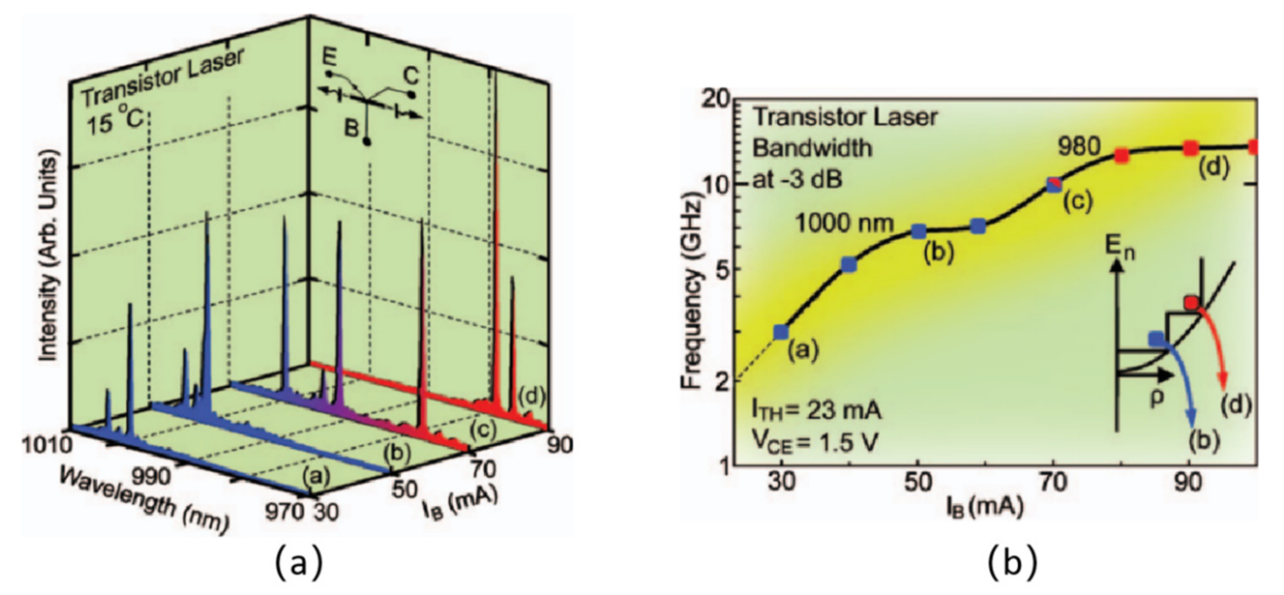
3.1.3. Main Excited State of QW as a Function of Current and Temperature

Different energy levels in the QW under different currents contribute differently to the optical gain due to their different gains [39]. Figure 6a presents the spectrum of the GaAs based TL current, lasing wavelength, and modulation bandwidth [40]. The lasing wavelength is blue-shifted with increasing external current. This is because under small implantation, the ground state energy level λ0 of GaAs based TL dominates the carrier recombination process. As shown in Figure 6b, the bandwidth growth trend of this device at low current is mainly determined by λ0. Although base current IB keeps increasing, λ0 binds the carriers more strongly and thus has a greater impact on the carrier transport. This leads to the gradual saturation of the modulation bandwidth controlled by λ0. Under a large injection, the main excitation energy level becomes the first excited state λ1, which has a weak ability to bind carriers; thus, the carrier transport process is further accelerated, the carrier recombination lifetime is further reduced, and a higher modulation bandwidth is obtained [41].
According to the report by Tan et al., as IB increases to 75 mA, the modulation bandwidth of a single QW-TL increases by 1.5 GHz. Further, the device achieved a no-error modulation signal transmission of 13.5 Gb/s at room temperature under this condition [42]. On a better bit error rate test equipment, the device achieved IB = 85 mA and 22 Gb/s no-error data transmission under the conditions of T = 15 °C and f-3 dB = 10.4 GHz [43].
In addition to the current, changes in the operating temperature also affect the lasing wavelength [44]. Figure 7a shows a temperature change I-V characteristics diagram of a GaAs based TL. With increasing temperature, the main excitation energy level changes (i.e., λ0 to λ1) and the electrical gain IC increases, which is manifested by the stretched IC-VCE characteristic curve shown in Figure 7a. With the injection unchanged, the increase in electrical gain indicates a decrease in optical gain (see Figure 7b). After the main excitation energy level was changed by heating, the light intensity was significantly reduced.
For InP based lasers, which are more commonly used in optical fiber communication, the variation law is different from that of GaAs lasers in terms of the excitation energy level with current and temperature. However, for InP based TLs, both the base current and the operating temperature red-shift the lasing wavelength—but for different reasons. The red-shift caused by the current change is due to the change in the excited state, and the main excited state gradually shifts from the first excited state to the ground state when the current increases [45]. In contrast, the red-shift caused by temperature changes is due to the power reduction resulting from the increase in the threshold current after the temperature rise [46].
The change in the main excited state reduces the single mode of the lasing light and the transmission ability of the signal. If TL is used for optical fiber communication, the base current and operating temperature should be properly regulated to avoid changes in excitation energy levels due to changes in these parameters, which will reduce the bandwidth and deteriorate single-mode properties.

3.2. Optimization of Each Layer in the Base Region

As shown in Figure 4b, the base region thickness (WB) is mainly composed of QW thickness (WQW), barrier width (Lb), and SCH layer thicknesses (WSCH1, WSCH2). The modulation speed of TL is highly dependent on the base region because both the recombination of carriers and the generation of light occur in the base region. The carrier transit time in the SCH layer, the recombination time within the QW, and the transit time between QWs affect both the photon generation and TL modulation rates. These parameters are closely related to the width of each layer structure in the base region. Therefore, the adjustment of the width of each structure in the base region to improve the modulation rate is feasible [47]. WQW affects the ability of QWs to trap and confine carriers. By changing WQW, the carrier recombination lifetime can be regulated and the relaxation oscillation can be adjusted. Lb determines the main mode of carrier transport between wells and the ratio of diffusion to tunneling. The SCH layer acts as a composition-changing layer to increase the additional potential energy and accelerate the transport of carriers, which can further improve the modulation bandwidth.

3.2.1. Base Thickness and Number of QWs

In more than a decade of research, owing to the differences in the material of TL devices and the number of QWs, the relationship between the tuning characteristics and the width of the base may be non-trivial.
Taghavi et al. (University of Illinois at Urbana-Champaign) conducted a detailed study on the effects of base variation in GaAs based TL [30]. For the MQW structure, the larger the WQW, the larger the transit time τc between wells, which is unfavorable for carrier transport. The wider the Lb, the larger the τc (until saturation); the reason why τc reaches saturation is that reaching a certain width diffusion completely replaces tunneling as the transport mode between wells. For different numbers of QWs, there exists an optimal WSCH that maximizes the modulation bandwidth. Habib et al. reported that this was due to the competition between the optical confinement factor and carrier transport [30]. At the SCH layer, tunneling gradually replaces diffusion as the main carrier injection method. Therefore, the transmission efficiency of the base region was significantly improved, the carrier lifetime was reduced, and the bandwidth was increased. However, the reduced photon confinement ability of the SCH layer results in a reduced photon concentration and bandwidth within the QW. The two variations compete with each other in the process of deriving the largest modulation bandwidth. The sudden decrease in bandwidth when the SCH layer reaches a certain thickness confirms the assumptions established in the previous analysis of the carrier transport model: because the increase in WB decreases the carrier transport rate and increases the radiative recombination lifetime, the competition between spontaneous emission and stimulated emission leads to a sudden decrease in bandwidth when the radiative lifetime exceeds a certain threshold. Further, in studying the modulation properties of GaAS based single QW–TL, Kaatuzian et al. came to similar conclusions as Taghavi et al., which means that there is a WB corresponding to the maximum modulation bandwidth [42]. The maximum bandwidth occurred at approximately WB = 100 nm. The optimal WB values reported by Tan et al. [47] and Habib et al. [30] were not identical possibly because of the differences in the material and structure of the device.
Subsequently, Kaatuzian et al. studied the modulation properties of InP based TL [48,49,50]. The effect of the WQW of InP based TL on the bandwidth was reported to be different from that of GaAs TL. The obvious difference is that the frequency of the InP based TL does not increase to the maximum peak with increasing WB but reaches saturation [49,50]. Besides, with increasing WB, the response curve reaches -3dB before the relaxation peak. This results in a sudden cutoff of the response frequency at WB = 300 nm, which is similar to that reported by Habib et al. [30].

3.2.2. Increasing the Potential of the SCH Layer Facilitates Carrier Transport

To further enhance the transport rate of carriers in the base region, changing the material mole fraction of the base region to reach a gradient that tilts the energy band can provide additional potential energy or an electric field that assists the carrier transport, which forms the SCH layer. In 2016, Hosseini et al. designed a GaAs based single QW-SCH structure [51]. The device changes the mole fraction of indium in the upper and lower base regions according to the gradient; the material of the top base region is InξGa1-ξAs (ξ: 0→0.029); the material of the bottom base region is InξGa1-ξAs (ξ: 0.038→0.05). Figure 8a is the original TL band structure. The rate of carrier movement from the emitter to the QW is accelerated owing to the band tilt, which reduces the recombination lifetime and base transit time of the carrier. This was the first application of the gradient-doped SCH structure to TL. The simulation results showed that the SCH layer can effectively reduce the base transit time due to the additional drift electric field and can increase the theoretical bandwidth of the TL from 69 GHz to 71 GHz.
In 2017, Hosseini et al. introduced the graded index (GRIN) SCH into TL; the band structure is shown in Figure 8b [52]. Compared with structure (3), structure (2) optimizes the mole fraction of the bottom base material (i.e., the mole fraction of indium changes from 0.02→0 to 0→0.02) and the mole fraction of the top base material (i.e., the mole fraction of indium changes from 0.07→0.02 to 0.05→0), which effectively improves the carrier capture ability of the QW. Considering the drift charge of the SCH layer, the simulated frequency response curve after modifying the charge continuity equation is shown in Figure 8d. Due to the change in the SCH2 energy band, the bandwidth of structure (2) is increased by 1.5 GHz compared to structure (3). As shown in Figure 8e, structure (2) also has a higher output power because the band structure of SCH2 provides an additional negative electric field for the carriers heading to the base region. Subsequently, this effectively improves the carrier confinement capability of the QW [53].
It was also reported that the threshold current of structure (2) is 6.5 mA, which is lower than that of structures (1) and (3). The report also stated that the current gain of Structure (3) is higher than that of Structure (1), which indicates that more carriers enter the collector rather than the QW. However, Structure (2) has the lowest current gain because the “funnel-shaped” energy band of Structure (2) suppresses carrier injection into the collector. The maximum output light intensity of Structure (2) in Figure 8e can also be explained by this point. This “funnel-shaped” energy band allows the carriers to be more strongly confined in the QW, where the carrier distribution is “peaked”. Although the current gain of Structure (3) is higher than that of Structure (1), more carriers enter the QW under the action of the base electric field of the GRIN-SCH layer. Consequently, the current gain and optical gain of Structure (3) are both higher than those of Structure (1). Further, the threshold current of Structure (3) is lower. Because Structure (3) has more carriers drifting into the collector, its threshold current is higher than that of Structure (2).
During their study of Structures (1) and (3), Hosseini et al. found that the introduction of the SCH2 layer brings significantly less bandwidth improvement than the SCH1 layer [54], which can be explained by the effect of the SCH layer on the carrier transport. The impact is mainly in the SCH1 layer. The main advantage of introducing the SCH2 layer is that it can increase the output optical power and reduce the threshold current. The report stated that the modulation bandwidth of GAIN-SCH–TL can be increased to approximately 100 GHz when combined with existing bandwidth enhancement techniques (e.g., the use of MQW structures and adjustment of QW positions).

3.2.3. Increased Carrier Injection Efficiency through SCH Tunneling

In DML, it is difficult to improve the modulation bandwidth because of the transport effect on carriers in QW [55]. To accelerate the carrier transport in DML and reduce the carrier lifetime, a tunnel injection (TI) structure that greatly weakens the carrier transport effect was invented [56]. An energy band diagram of the structure is shown in Figure 9 [57]. In the TI structure, tunneling is the main carrier transport from the emitter to the first QW. Subsequently, the carriers between the wells are transported through a mixture of tunneling and diffusion, which significantly reduces the auger recombination and increases the efficiency of the radiative transition and output light intensity. Overall, the modulation bandwidth of the TI-DML is larger than that of conventional DML.
Based on their research on TI-DML, Rikmantra et al. predicted that the bandwidth of TI–TL can be significantly better than that of conventional TL [38]. Subsequent studies have demonstrated that the bandwidth of TI–TL is 44 GHz, which is higher than the 29 GHz bandwidth of conventional TL [58].
The tunneling properties of TI–TL were also studied extensively by Neetesh et al. [59]. They noted that the tunneling structure considerably reduced the threshold current and increased the modulation bandwidth compared with conventional MQW–TL structure. This change is more pronounced as the tunneling probability f (i.e., 0 ≤ f ≤ 1) increases, which characterizes the probability of the charge carriers tunneling into the first QW from the upper base SCH layer. The simulation shows that increasing f increases the modulation bandwidth [59]. When no tunnel structure is added at f = 0, all carriers enter the QW by diffusion, and the bandwidth is 29.01 GHz. As f increases, due to the tunneling effect, the number of carriers entering the QW increases, the transport process is accelerated, the recombination lifetime decreases, and the relaxation frequency and bandwidth increase. In the ideal case (f = 1), all carriers are tunneled into the QW; in this case, the bandwidth reaches a maximum of 56 GHz. Noted that the peak amplitude of the relaxation oscillation increases by approximately 3 dB as f goes from zero to one. In theory, this is not suitable for signal fidelity. Therefore, in the process of transmitting signals using TI–TL, the trade-off between the relaxation peak amplitude and modulation bandwidth must be considered.
As f increases from zero to one, the second harmonic distortion decreases, and the third-order intermodulation distortion (IMD3) is reduced from −27.17 to −39.42 dBm, while the fifth-order intermodulation distortion (IMD5) is reduced from −43.59 to −48.5 dBm. This proves that the distortion of the signal is suppressed as tunneling occurs [60].

3.3. Intracavity Photon-Assisted Tunneling

By applying heavy doping to the collector and bottom base materials, Feng et al. reported an intracavity photon-assisted tunneling transistor laser (ICPAT–TL; hereinafter, tunnel junction transistor laser (TJ–TL)) [61]. This process is called the Franz–Keldysh intracavity photon-assisted tunneling because of the use of the Franz–Keldysh effect. The basic process of Franz–Keldysh photon-assisted tunneling involves applying a voltage at the collector–base interface to change the energy band of the transition region, which causes the top carriers of the valence band to transition to the bottom of the conduction band by absorbing the photons emitted by the QW; the excess holes diffuse to the QW valence band and promote the occurrence of radiative transitions within the QW (see Figure 10). This is a self-regulating process of reorganization and absorption, which guarantees that ΔIE = ΔIC and IB is constant [62]. The concept of a TL voltage-driven switch that converts stimulated emission (highly coherent light field) to spontaneous emission (low incoherent light field) was demonstrated using the Franz-Keldysh photon-assisted process [63].
Although the modulation bandwidth of TL cannot be directly improved by FK photon-assisted tunneling, it is possible to directly modulate the voltage using transition region tunneling (IrT) and strong FK transition (IfkT) coupled to the radiative transition inside the QW. FK photon-assisted tunneling enables the modulation of light output by changing the collector voltage rather than only by current modulation. Compared with increasing the bandwidth, FK photon-assisted tunneling has a greater impact on the output power. The output power of TL devices reported to date cannot meet the demands of optical fiber communication; thus, FK photon-assisted tunneling is an important research direction for improving TL power output.
The reason why FK photon-assisted tunneling can regulate the optical power by changing the voltage can be determined by analyzing Figure 11a. In region (1), during the TJ–TL operation under a weak collector junction field, collector tunneling enables holes to be effectively supplied to the active QW region (i.e., IfkT > 0, photon-assisted tunneling occurs), thereby increasing the laser output light quantity. In region (2), the voltage exceeds 0.8 V, and then the output light intensity of the device weakens owing to the FK light absorption effect. Because the output light intensity of TJ–TL can be easily regulated through voltage control, TJ–TL can be directly modulated through current and voltage controls. The sensitivity of optical power to VCE changes is shown in Figure 11b [64]. It shows that as IB increases, the curve of the light intensity change ΔL versus VCB becomes steeper. This shows that TJ–TL can be used for high-speed optoelectronic devices (e.g., optical switches) and voltage modulation. Compared to current modulation, voltage modulation is easier to implement in integrated circuits. Therefore, TJ–TL should be considered in future modulation schemes for optical fiber transmission.
As reported by Tung et al. [65], the bandwidth of the current modulation is higher than that of the voltage modulation. However, the peak frequency amplitude of the voltage modulation is flatter due to the sloping distribution of the base carrier density and the collector voltage-controlled photon absorption (i.e., FK tunneling), which eliminates charge accumulation. It follows that the voltage modulation has a wider adjustable frequency range and lower error rate [65].
In microwave photonic links, the TL of the current modulation is similar to that of the traditional DML, and the modulation frequency cannot be higher than the relaxation frequency fR in practical applications. In contrast, although the bandwidth of the voltage modulation is small, the frequency response up to f-3 dB is flat. Therefore, voltage modulation may be more suitable for high-speed signal transmission than current modulation. Further, the input resistance of voltage modulation is higher than that of current modulation, which makes it easier to match with the external resistance. It must be noted that the conditions for the analysis are that the bias is different and the output power is the same. Current modulation is better than voltage modulation in resistance matching when current and voltage modulations are under the same bias conditions [66].
The bandwidth variation trend with respect to IB and VCB under the two modulation schemes differs [67,68]. In the current modulation process, as IB increases, the number of photons increases and the bandwidth increases. However, at large injections, the photon concentration is notably reduced owing to thermal effects, making it difficult to increase the bandwidth. In the process of voltage modulation, as VCB increases, the modulation bandwidth decreases. Under high reverse-biased VCB, the photon density and modulation bandwidth are considerably reduced due to the significant FK absorption effect.
In the analysis of the voltage modulation response curve, in addition to the inherent optical response, it is also necessary to consider the electronic transfer function of the optical response feedback; otherwise, it will lead to a large AC enhancement peak on the voltage modulation response curve [67]. The amplitude of the relaxation oscillation of the voltage modulation is greatly reduced after the introduction of the electron transfer function.
According to Tung et al. [69], under the same bias condition, the bandwidth in the voltage modulation case can reach more than 21.4 GHz, which can achieve a 30 Gb/s data transmission rate. In contrast, the bandwidth in the current modulation case is only 5.5 GHz, which can only achieve a 10 Gb/s data transmission rate.
The voltage modulation of TL is more complicated than of the current modulation model due to FK absorption. Changes in the current IB and voltage VCB cause chirp in the TL [70]. Although the chirp produced by current modulation is similar to the DML case, the chirp produced by voltage modulation is different. Changes in the FK absorption coefficient and the base refractive index cause chirping with the change in VCB. In the photon-assisted process, the holes generated in the valence band of the transition region diffuse into the active region and then change the carrier density distribution in the QW, which can also cause chirping [71].
Tung et al. proposed and modeled a dual-and-direct current–voltage modulation method to solve the chirp problem that occurs in TL voltage modulation [72]. The scheme is based on the opposite frequency shifts produced by current modulation and voltage modulation. The aim is to induce chirps during modulation through IB and VCB such that they negate each other. Let Δν denote the total instantaneous frequency shift due to modulation; the frequency shift due to current modulation is Δν(I) and that due to voltage modulation is Δν(V) (i.e., Δν = Δν(I) + Δν(V)).
When IB is fixed on IB(zc), which is obtained from the zero-chirp case, and the voltage signal weight of VCB is changed, the voltage change ΔVCB is as follows:
Δ V C B = Δ V C B m 1 m Δ V 0 + m Δ V C B z c ,
where ΔVCB(m) is the weighted voltage signal, ΔV0 is the constant portion of ΔVCB(zc) before pulse generation, and ΔVCB(zc) is the VCB at zero chirp. A large m (0 ≤ m ≤ 1) indicates more chirp cancellation and a greater voltage weight.
As Δν(V) increases, and ΔVCB and Δν(I) negate each other more, the overall frequency shift and number of chirps are smaller. Moreover, the weakening of the FK absorption due to the decrease in VCB increases the output light intensity. In this study, the simulated eye diagrams for a 10 Gb/s data transmission rate is still clear after transmitting 100 km with zero chirp (i.e., m = 1) and a pulse width of 0.1 ns.
The TJ–TL collector doping has a significant influence on the voltage modulation capability [73] due to its dependence on the base-collector junction field. With heavy doping of the collector region, the enhanced junction field and FK absorption reduce the output optical power, which reduces the bandwidth. However, heavy doping also increases the sensitivity of FK absorption to voltage, which implies that an increase in the sensitivity of the optical power to VCB changes and modulation speed. The collector doping density must be carefully considered because of the trade-off between power and modulation sensitivity. The chosen doping density value should ensure sufficient optical power and photon density while improving the sensitivity to voltage modulation.
The discovery and application of photon-assisted tunneling have considerably expanded the application prospects of TL in laser modulation. Further, they also confirmed the great potential of TL in the future application of high-speed optoelectronic devices. However, the modulation characteristics of TJ–TL are significantly more complicated than those of conventional TL.

3.4. Auxiliary for External Circuits

3.4.1. Increase the Bandwidth by Applying the Base Auxiliary Signal

The unique three-electrode structure of TL offers the potential to control and improve the light output characteristics through external measures. Because carriers are injected into the electrical collector (i.e., QW) at a longer distance than that of the optical collector during transport, it leads to a phenomenon wherein the electrical gain is slower than the optical gain. In the case of a certain number of injected carriers, if the probability of carrier recombination in the QW is increased by some means, the time to reach the peak light intensity and the overall response time will be shortened [74], which will lead to a decrease in electrical gain. Then et al. proposed the use of a low-frequency AC base auxiliary signal to enhance the carrier transport to the QW. More carriers are guided into the QW as the applied AC signal suppresses the electrical gain in the collector, which improves the differential gain of the laser, accelerates the optical response, and increases the bandwidth. Figure 12 shows the proposed circuit diagram by Then et al. After applying an AC auxiliary signal of 9 MHz, the modulation bandwidth of the TL was increased to 22 GHz, which is 11.5 GHz higher than the response bandwidth without the AC signal.
Then et al. demonstrated that the electrical and optical gains are coupled in TL; thus the differential optical gain, photon density, and modulation bandwidth can be improved by the photon–electron “trade-off” [75], which provides a new way to improve the TL modulation rate. This trade-off is somewhat similar to the previously mentioned trade-off of bandwidth and electrical gain, but the regulation mechanisms different. Whereas the “trade-off” mentioned in Section 3.1.2 is achieved by changing the QW position, the “trade-off” here increases the bandwidth by suppressing the current gain by the AC signal.

3.4.2. Predistortion Network

Owing to the nonlinear characteristics of the TL, the base current generates harmonics and intermodulation distortion during input, among which the IMD3 has the greatest impact on the link transmission signal.
To suppress signal distortion, Vinodhini et al. first reported a TL predistortion network technique based on the Schottky diode nonlinear compensation [76]. The modulated signal undergoes a 180° phase change after passing through the Schottky diode. Subsequently, it is superimposed with the signal passing through the delay line, which can use the phase difference to cancel the IMD3 component of the modulated signal. However, a one-Schottky diode circuit can limit the bandwidth owing to the use of phase shifters. To overcome this, a dual Schottky diode circuit can be used, which utilizes two Schottky diodes with an antiparallel structure to reduce the intermodulation distortion component by adjusting their bias currents.
Without the Schottky diode predistortion network, the output spectrum exhibits a magnitude difference of 15.92 dBc between the input frequency and the IMD3 component. Because the IMD3 of the TL varies with the bias current, adjusting the bias voltage of the Schottky diode to make its nonlinearity the same as that of the TL can reduce the IMD3. After joining the network, the IMD3 component was notably reduced. The amplitude difference between the input frequency and the IMD3 component is 29.48 dBc under the single Schottky network and 31.45 dBc under the double Schottky network.
After adding the predistortion network, the IMD3 component was reduced and the bandwidth was increased. One and dual Schottky diode predistortion techniques increased the bandwidth to 12 and 13.8 GHz, respectively. Under the same bias condition, the bandwidth without predistortion network analysis was only 10.96 GHz. However, when the predistortion network was introduced, the relaxation peak amplitude increased. This increase needs to be reduced for the optimization of this technology.

4. Conclusions

Owing to the rapid recombination of base region carriers, TL shows enormous potential in the field of optical fiber communication. The design of TL for fast data transfer must consider the parameters of the epitaxial chip. Further, the introduction of the predistortion network and base region signal assist also affect the fast modulation performance of the TL. The modulation bandwidth of TL is enhanced by the fast removal of carriers in the base region, but the output optical power of TL will be reduced for the carrier loss. The output power of the TL is improved with photon-assisted tunneling; thus, TJ–TL is the key step that will allow the practical application of TLs. The results of these studies are shown in Table 1.
DML also suggests many ways to improve the modulation characteristics, as shown in Table 2. These methods are not only likely to be applicable to TL, but can also possibly be combined with the unique three-electrode structure of TL. Table 1 and Table 2 summarize the progress of TL and DML modulation characteristics technology over the past decade, respectively. It can be clearly seen that the modulation characteristic of DML is much better than that of TL. This is because TL was only invented in 2004, and most of the theoretical research on TL still needs to be experimentally confirmed, which also demonstrates the great potential of TL.

Author Contributions

Conceptualization, L.F. and L.Q.; methodology, Q.C. and Y.L.; validation, P.J. and Y.C.; formal analysis, L.F. and P.J.; investigation, P.J., C.Q. and Y.L.; resources, L.F., Y.W. and Y.S.; writing—original draft preparation, L.F.; writing—review and editing, Y.C.; supervision, Y.C. and L.L.; project administration, Y.N.; funding acquisition, L.Q. and L.W. All authors have read and agreed to the published version of the manuscript.

Funding

This research was funded by the National Key R & D Program of China, grant number 2018YFB2200300; the National Natural Science Foundation of China, grant numbers 11874353, 61904179, 62090054, 61934003, 62090052, and 62090051; the Science and Technology Development Project of Jilin Province, grant numbers 202001069GX, 20200501006GX, 20200501007GX, and 20200501008GX; the Dawn Talent Training Program of CIOMP; the National Science and Technology Major Project of China, grant numbers 2018YFB0504600 and 2018YFB0504603; the National Natural Science Foundation of China (NSFC), grant numbers 62090051, 62090052, 62090054, 11874353, 61935009, 61934003, 61904179, 61727822, 61805236, and 62004194; the Science and Technology Development Project of Jilin Province, grant numbers 20200401069GX, 20200401062GX, 20200501006GX, 20200501007GX, and 20200501008GX; the Key R&D Program of Changchun, grant number 21ZGG13; the Special Scientific Research Project of Academician Innovation Platform in Hainan Province, grant number YSPTZX202034; and the “Lingyan” Research Program of Zhejiang Province, grant number 2022C01108.

Institutional Review Board Statement

Not applicable.

Informed Consent Statement

Not applicable.

Data Availability Statement

Not applicable.

Acknowledgments

The authors thank Yongqiang Ning, Lijun Wang, Lei Liang, Cheng Qiu, Xing Zhang, and Xia Liu for helping with this article.

Conflicts of Interest

The authors declare no conflict of interest.

References

  1. Katz, J.; Bar-Chaim, N.; Chen, P.C.; Margalit, S.; Ury, I.; Wilt, D.; Yust, M.; Yariv, A. A monolithic integration of GaAs/GaAlAs bipolar transistor and heterostructure laser. Appl. Phys. Lett. 1980, 37, 211–213. [Google Scholar] [CrossRef] [Green Version]
  2. Shibata, J.; Nakao, I.; Sasai, Y.; Kimura, S.; Hase, N.; Serizawa, H. Monolithic integration of an InGaAsP/InP laser diode with heterojunction bipolar transistors. Appl. Phys. Lett. 1984, 45, 191–193. [Google Scholar] [CrossRef] [Green Version]
  3. Mori, Y.; Shibata, J.; Sasai, Y.; Serizawa, H.; Kajiwara, T. Operation principle of the InGaAsP/InP laser transistor. Appl. Phys. Lett. 1985, 47, 649–651. [Google Scholar] [CrossRef]
  4. Shibata, J.; Mori, Y.; Sasai, Y.; Hase, N.; Serizawa, H.; Kajiwara, T. Fundamental characteristics of an ingaasp/inp laser transistor. Electron. Lett. 1985, 21, 98–100. [Google Scholar] [CrossRef]
  5. Holonyak, N.; Feng, M. The transistor laser. IEEE Spectr. 2006, 43, 50–55. [Google Scholar] [CrossRef]
  6. Khorasani, M.; Ghasemi, A.; Rolfe, B.; Gibson, I. Additive manufacturing a powerful tool for the aerospace industry. Rapid Prototyp. J. 2022, 28, 87–100. [Google Scholar] [CrossRef]
  7. Hung, C.-H.; Turk, T.; Sehhat, M.H.; Leu, M.C. Development and experimental study of an automated laser-foil-printing additive manufacturing system. Rapid Prototyp. J. 2022, ahead-of-print. [Google Scholar] [CrossRef]
  8. Khan, H.M.; Waqar, S.; Koç, E. Evolution of temperature and residual stress behavior in selective laser melting of 316l stainless steel across a cooling channel. Rapid Prototyp. J. 2022, ahead-of-print. [Google Scholar] [CrossRef]
  9. Linares, J.-m.; Chaves-Jacob, J.; Lopez, Q.; Sprauel, J.-M. Fatigue life optimization for 17-4ph steel produced by selective laser melting. Rapid Prototyp. J. 2022, ahead-of-print. [Google Scholar] [CrossRef]
  10. Giganto, S.; Martínez-Pellitero, S.; Cuesta, E.; Zapico, P.; Barreiro, J. Proposal of design rules for improving the accuracy of selective laser melting (slm) manufacturing using benchmarks parts. Rapid Prototyp. J. 2022, ahead-of-print. [Google Scholar] [CrossRef]
  11. Then, H.W.; Feng, M.; Holonyak, N.; Wu, C.H. Experimental determination of the effective minority carrier lifetime in the operation of a quantum-well n-p-n heterojunction bipolar light-emitting transistor of varying base quantum-well design and doping. Appl. Phys. Lett. 2007, 91, 033505. [Google Scholar] [CrossRef]
  12. Winoto, A.; Qiu, J.; Wu, D.; Feng, M. Transistor Laser-Integrated Photonics for Optical Logic: Unlocking Unique Electro-Optical Integration Potential to Open Up New Possibilities for Logic Processors. IEEE Nanotechnol. Mag. 2019, 13, 27–34. [Google Scholar] [CrossRef]
  13. Tan, F.; Bambery, R.; Feng, M.; Holonyak, N. Transistor laser with simultaneous electrical and optical output at 20 and 40 Gb/s data rate modulation. Appl. Phys. Lett. 2011, 99, 061105. [Google Scholar] [CrossRef]
  14. Wu, M.K. Development of Vertical Cavity Transistor Laser and Microcavity Laser. Ph.D. Thesis, University of Illinois at Urbana-Champaign, Urbana-Champaign, IL, USA, 2014. Available online: http://hdl.handle.net/2142/49650 (accessed on 14 January 2022).
  15. Sasada, N.; Nakajima, T.; Sekino, Y.; Nakanishi, A.; Mukaikubo, M.; Ebisu, M.; Mitaki, M.; Hayakawa, S.; Naoe, K. Wide-Temperature-Range (25–80 °C) 53-Gbaud PAM4 (106-Gb/s) Operation of 1.3-μM Directly Modulated DFB Lasers for 10-km Transmission. J. Lightwave Technol. 2019, 37, 1686–1689. [Google Scholar] [CrossRef]
  16. Shahin, M.; Ma, K.; Abbasi, A.; Roelkens, G.; Morthier, G. 45 Gb/s Direct Modulation of Two-Section InP-on-Si DFB Laser Diodes. IEEE Photonics Technol. Lett. 2018, 30, 685–687. [Google Scholar] [CrossRef] [Green Version]
  17. Huang, Y.; Ryou, J.-H.; Dupuis, R.D.; Dixon, F.; Feng, M.; Holonyak, N. InP/InAlGaAs light-emitting transistors and transistor lasers with a carbon-doped base layer. J. Appl. Phys. 2011, 109, 063106. [Google Scholar] [CrossRef]
  18. Taylor, J.; Tolstikhin, V. Intervalence band absorption in InP and related materials for optoelectronic device modeling. J. Appl. Phys. 2000, 87, 1054–1059. [Google Scholar] [CrossRef]
  19. Feng, M.; Holonyak, N.; Chan, R. Quantum-well-base heterojunction bipolar light-emitting transistor. Appl. Phys. Lett. 2004, 84, 1952–1954. [Google Scholar] [CrossRef]
  20. Chan, R.; Feng, M.; Holonyak, N.; Walter, G. Microwave operation and modulation of a transistor laser. Appl. Phys. Lett. 2005, 86, 131114. [Google Scholar] [CrossRef]
  21. Feng, M.; Holonyak, N.; Walter, G.; Chan, R. Room temperature continuous wave operation of a heterojunction bipolar transistor laser. Appl. Phys. Lett. 2005, 87, 131103. [Google Scholar] [CrossRef]
  22. Zhang, P.N. Research on Mid-Infared Transistor-Injected Quantum Cascade Laser and Its Characteristics. Master’s Thesis, University of Electronic Science and Technology of China, Chengdu, China, 2020. [Google Scholar] [CrossRef]
  23. Feng, M.; Then, H.W.; Holonyak, N.; Walter, G.; James, A. Resonance-free frequency response of a semiconductor laser. Appl. Phys. Lett. 2009, 95, 033509. [Google Scholar] [CrossRef]
  24. Feng, M.; Holonyak, N.; Then, H.W.; Walter, G. Charge control analysis of transistor laser operation. Appl. Phys. Lett. 2007, 91, 053501. [Google Scholar] [CrossRef]
  25. Li, Y.; Leburton, J.-P. Base transport factor and frequency response of transistor lasers. J. Appl. Phys. 2019, 126, 153103. [Google Scholar] [CrossRef]
  26. Taghavi, I.; Kaatuzian, H.; Leburton, J.-P. Multiple versus Single Quantum Well Transistor Laser Performances. In Proceedings of the Advanced Photonics Congress, Colorado Springs, Colorado, 17 June 2012; p. IM4B.5. [Google Scholar] [CrossRef]
  27. Lu, D.; Yang, Q.L.; Wang, H.; He, Y.M.; Qi, H.F.; Wang, H.; Zhao, L.J.; Wang, W. Review of Semiconductor Distributed Feedback Lasers in the Optical Communication Band. Chin. J. Lasers 2020, 47, 0701001. [Google Scholar] [CrossRef]
  28. Xu, G.; Huang, C.; Liu, Q.; Liu, R.; Chai, G.; Duan, Z. One-dimensional numerical analysis of transistor lasers. Opt. Quantum Electron. 2012, 45, 87–96. [Google Scholar] [CrossRef]
  29. Nagarajan, R.; Ishikawa, M.; Fukushima, T.; Geels, R.S.; Bowers, J.E. High-speed quantum-well lasers and carrier transport effects. IEEE J. Quantum Electron. 1992, 28, 1990–2008. [Google Scholar] [CrossRef]
  30. Taghavi, I.; Kaatuzian, H.; Leburton, J.-P. Performance Optimization of Multiple Quantum Well Transistor Laser. IEEE J. Quantum Electron. 2013, 49, 426–435. [Google Scholar] [CrossRef]
  31. Taghavi, I.; Kaatuzian, H.; Leburton, J.-P. Bandwidth enhancement and optical performances of multiple quantum well transistor lasers. Appl. Phys. Lett. 2012, 100, 231114. [Google Scholar] [CrossRef] [Green Version]
  32. Kaatuzian, H.; Taghavi, I.; Danayee, M.; IEEE. Dependence of Transistor Laser Optical Frequency Response on Quantum-Well Position. In Proceedings of the International Conference on Recent Advances in Microwave Theory and Applications, Jaipur, India, 21–24 November 2008; pp. 406–409. [Google Scholar] [CrossRef]
  33. Taghavi, I.; Kaatuzian, H. Gain-bandwidth trade-off in a transistor laser: Quantum well dislocation effect. Opt. Quant. Electron. 2010, 41, 481–488. [Google Scholar] [CrossRef]
  34. Kaatuzian, H.; Taghavi, I.; Danaie, M.; AOE. Effects of Quantum-Well Displacement on Optical Frequency Response of a Transistor Laser. In Proceedings of the AOE 2008: Asia Optical Fiber Communication and Optoelectronic Exposition and Conference, Shanghai, China, 30 October–2 November 2008. [Google Scholar]
  35. Habib, M.A.; Das, S.; Ullah, S.M.; Rafique, S. Optimal quantum well width and the effect of quantum well position on the performance of transistor lasers. Optoelectron. Lett. 2013, 9, 18–20. [Google Scholar] [CrossRef]
  36. Taghavi, I.; Kaatuzian, H. A numerical study on base geometry of transistor laser: Quantum-well location effect. In Proceedings of the Electrical Engineering, Bandung, Indonesia, 17–19 July 2011. [Google Scholar]
  37. Taghavi, I.; Aa Tuzian, H.K. Optical Bandwidth Optimization in a Transistor Laser by Quantum Well Location Effect. In Proceedings of the Photonics and Optoelectronic (SOPO), Chengdu, China, 19–21 June 2010. [Google Scholar] [CrossRef]
  38. Basu, R.; Mukhopadhyay, B.; Basu, P.K. Modeling Resonance-Free Modulation Response in Transistor Lasers with Single and Multiple Quantum Wells in the Base. IEEE Photon. J. 2012, 4, 1572–1581. [Google Scholar] [CrossRef]
  39. Then, H.W.; Feng, M.; Holonyak, N. Optical bandwidth enhancement by operation and modulation of the first excited state of a transistor laser. Appl. Phys. Lett. 2007, 91, 183505. [Google Scholar] [CrossRef]
  40. Feng, M.; Holonyak, N.; James, A.; Cimino, K.; Walter, G.; Chan, R. Carrier lifetime and modulation bandwidth of a quantum well AlGaAs∕InGaP∕GaAs∕InGaAs transistor laser. Appl. Phys. Lett. 2006, 89, 113504. [Google Scholar] [CrossRef]
  41. Bambery, R.; Wang, C.; Dallesasse, J.M.; Feng, M.; Holonyak, N. Effect of the energy barrier in the base of the transistor laser on the recombination lifetime. Appl. Phys. Lett. 2014, 104, 081117. [Google Scholar] [CrossRef]
  42. Tan, F.; Bambery, R.; Feng, M.; Holonyak, N. Transistor Laser with 13.5-Gb/s Error-Free Data Transmission. IEEE Photonics Technol. Lett. 2014, 26, 1542–1545. [Google Scholar] [CrossRef]
  43. Bambery, R.; Wang, C.Y.; Tan, F.; Feng, M.; Holonyak, N. Single Quantum-Well Transistor Lasers Operating Error-Free at 22 Gb/s. IEEE Photonics Technol. Lett. 2015, 27, 600–603. [Google Scholar] [CrossRef]
  44. Feng, M.; Holonyak, N.; James, A. Temperature dependence of a high-performance narrow-stripe (1 μM) single quantum-well transistor laser. Appl. Phys. Lett. 2011, 98, 051107. [Google Scholar] [CrossRef]
  45. Qiao, L.J.; Liang, S.; Han, J.J. Continuous-wave operation up to 20 degrees C of deep-ridge npn-InGaAsP/InP multiple quantum well transistor laser emitting at 1.5-mum wavelength. Opt. Express 2015, 23, 11388–11393. [Google Scholar] [CrossRef]
  46. Liang, S.; Kong, D.H.; Zhu, H.L.; Zhao, L.J.; Pan, J.Q.; Wang, W. InP-based deep-ridge NPN transistor laser. Opt. Lett. 2011, 36, 3206–3208. [Google Scholar] [CrossRef]
  47. Kaatuzian, H.; Mojaver, H.R.; Taghavi, I. Optical Modulation Bandwidth Enhancement of Heterojunction Bipolar Transistor Lasers Using Base Width Variation. In Proceedings of the 2011 Numerical Simulation of Optoelectronic Devices, Rome, Italy, 5–8 September 2012. [Google Scholar]
  48. Mojaver, H.R.; Kaatuzian, H. Analysis and improvement of optical frequency response in a long wavelength transistor laser. Opt. Quantum Electron. 2011, 44, 45–54. [Google Scholar] [CrossRef]
  49. Farjadian, M.R.; Kaatuzian, H.; Taghavi, I. The Effects of Base width variation on Resonance Behavior of Double-Hetero Structure Long Wavelength Transistor Laser. In Proceedings of the 22nd Iranian Conference on Electrical Engineering, Tehran, Iran, 5 January 2015. [Google Scholar] [CrossRef]
  50. Farjadian, M.R.; Kaatuzian, H.; Taghavi, I. Theoretical analysis on optoelectronic performances of long wavelength transistor lasers: Base width variation effects. Opt. Quantum Electron. 2014, 46, 871–881. [Google Scholar] [CrossRef]
  51. Hosseini, M.; Kaatuzian, H.; Taghavi, I. Design and analysis of GRIN-SCH-SQW transistor laser. In Proceedings of the 24th Iranian Conference on Electrical Engineering, Shiraz, Iran, 10 October 2016. [Google Scholar] [CrossRef]
  52. Hosseini, M.; Kaatuzian, H.; Taghavi, I. Graded index separate confinement heterostructure transistor laser: Analysis of various confinement structures. Chin. Opt. Lett. 2017, 15, 062501. [Google Scholar] [CrossRef]
  53. Hosseini, M.; Kaatuzian, H.; Taghavi, I. Investigation of confining layers effects on optoelectronic performances of transistor laser. In Proceedings of the 25th Iranian Conference on Electrical Engineering, Tehran, Iran, 20 July 2017. [Google Scholar] [CrossRef]
  54. Hosseini, M.; Kaatuzian, H.; Taghavi, I.; Ghodsi, H. Efficient carrier transport in GRIN-SCH transistor lasers. Quantum Electron. 2019, 49, 391–398. [Google Scholar] [CrossRef]
  55. Chen, Y.; Wartak, M.S.; Lu, H.; Makino, T. Investigation of carrier transport effects in multiple-quantum-well lasers. J. Appl. Phys. 1995, 78, 5515–5517. [Google Scholar] [CrossRef]
  56. Bhattacharya, P.; Singh, J.; Yoon, H.; Zhang, X.K.; Gutierrez-Aitken, A.; Lam, Y. Tunneling injection lasers: A new class of lasers with reduced hot carrier effects. IEEE J. Quantum Electron. 1996, 32, 1620–1629. [Google Scholar] [CrossRef]
  57. Rusek, P.; Wartak, M.S.; Weetman, H. Modulation response of tunneling injection laser: Analytical approach. IEEE J. Quantum Electron. 1998, 84, 5419–5423. [Google Scholar] [CrossRef]
  58. Basu, R.; Mukhopadhyay, B.; Basu, P.K. Performance Study of a Tunnel Injection Transistor Laser with Multiple Quantum-Wells in the Base. In Proceedings of the 12th International Conference on Fiber Optics and Photonics, Kharagpur, India, 13 December 2014. [Google Scholar] [CrossRef]
  59. Kumar, N.; Mukhopadhyay, B.; Basu, R. Tunnel injection transistor laser for optical interconnects. Opt. Quantum Electron. 2018, 50, 160. [Google Scholar] [CrossRef]
  60. Vinodhini, S.V.; Piramasubramanian, S. Effect of tunneling probability on the distortion characteristics of tunnel injection transistor laser. Opt. Commun. 2020, 460, 1–8. [Google Scholar] [CrossRef]
  61. Feng, M.; Holonyak, N.; Then, H.W.; Wu, C.H.; Walter, G. Tunnel junction transistor laser. Appl. Phys. Lett. 2009, 94, 041118. [Google Scholar] [CrossRef]
  62. James, A.; Walter, G.; Feng, M.; Holonyak, N. Photon-assisted breakdown, negative resistance, and switching in a quantum-well transistor laser. Appl. Phys. Lett. 2007, 90, 091109. [Google Scholar] [CrossRef]
  63. James, A.; Holonyak, N.; Feng, M.; Walter, G. Franz–Keldysh Photon-Assisted Voltage-Operated Switching of a Transistor Laser. IEEE Photonics Technol. Lett. 2007, 19, 680–682. [Google Scholar] [CrossRef]
  64. Feng, M.; Qiu, J.; Wang, C.Y.; Holonyak, N. Intra-cavity photon-assisted tunneling collector-base voltage-mediated electron-hole spontaneous-stimulated recombination transistor laser. J. Appl. Phys. 2016, 119, 084502. [Google Scholar] [CrossRef]
  65. Then, H.W.; Feng, M.; Holonyak, N. The Transistor Laser: Theory and Experiment. Proc. IEEE 2013, 101, 2271–2298. [Google Scholar] [CrossRef]
  66. Iezekiel, S.; Christou, A. Microwave Photonic Links Based on Transistor Lasers: Voltage Modulation versus Current Modulation. In Proceedings of the International Topical Meeting on Microwave Photonics and the 2014 9th Asia-Pacific Microwave Photonics Conference, Hokkaido, Japan, 22 December 2014. [Google Scholar] [CrossRef]
  67. Chang, C.H.; Chang, S.W.; Wu, C.H. Theory for voltage modulation of transistor lasers using Franz-Keldysh absorption in the presence of optoelectronic feedback. Opt. Express 2016, 24, 25515–25527. [Google Scholar] [CrossRef]
  68. Ramya, R.; Piramasubramanian, S. Effect of Franz–Keldysh absorption on the short optical pulse generation in Transistor Laser. Opt. Commun. 2020, 474, 1–8. [Google Scholar] [CrossRef]
  69. Tung, C.T.; Chang, S.W.; Wu, C.H. High Speed Data Transmission under Voltage Modulation of Transistor Lasers. In Proceedings of the 23rd Opto-Electronics and Communications Conference, Jeju, Korea, 6 June 2019. [Google Scholar] [CrossRef]
  70. Tung, C.T.; Chang, C.H.; Chang, S.W.; Wu, C.H. Pulse compression irrespective of fiber dispersion using chirp of transistor lasers. Opt. Lett. 2019, 44, 2109–2112. [Google Scholar] [CrossRef]
  71. Feng, M.; Qiu, J.; Wang, C.H.; Holonyak, N. Tunneling modulation of a quantum-well transistor laser. J. Appl. Phys. 2016, 120, 084502. [Google Scholar] [CrossRef]
  72. Tung, C.T.; Chang, S.W.; Wu, C.H. Chirp-free optical-signal generation using dual-and-direct current-voltage modulation of transistor lasers. Opt. Lett. 2020, 45, 2474–2477. [Google Scholar] [CrossRef]
  73. Tung, C.T.; Lin, H.Y.; Chang, S.W.; Wu, C.H. Analytical Modeling of Tunnel-Junction Transistor Lasers. IEEE J. Sel. Top. Quantum Electron. 2016, 24, 25515–25527. [Google Scholar] [CrossRef]
  74. Then, H.W.; Walter, G.; Feng, M.; Holonyak, N. Optical bandwidth enhancement of heterojunction bipolar transistor laser operation with an auxiliary base signal. Appl. Phys. Lett. 2008, 93, 091109. [Google Scholar] [CrossRef]
  75. Then, H.W.; Feng, M.; Holonyak, N. Bandwidth extension by trade-off of electrical and optical gain in a transistor laser: Three-terminal control. Appl. Phys. Lett. 2009, 94, 013509. [Google Scholar] [CrossRef]
  76. Vinodlhini, S.V.; Piramasubramanian, S.; Madhan, M.G.; Sandhiya, M. Analysis of distortion reduction in 1.3 μM transistor laser using Schottky diode based predistortion network. Optik 2007, 231, 051107. [Google Scholar] [CrossRef]
  77. Bambery, R.; Tan, F.; Feng, M.; Dallesasse, J.M.; Holonyak, N. Voltage and current modulation at 20 Gb/s of a transistor laser at room temperature. IEEE Photonics Technol. Lett. 2013, 25, 859–862. [Google Scholar] [CrossRef]
  78. Kobayashi, W.; Ito, T.; Yamanaka, T.; Fujisawa, T.; Shibata, Y.; Kurosaki, T.; Kohtoku, M.; Tadokoro, T.; Sanjoh, H. 50-Gb/s direct modulation of a 1.3-mu m InGaAlAs-based DFB laser with a ridge waveguide structure. IEEE J. Sel. Top. Quantum Electron. 2013, 19, 500908–1500908. [Google Scholar] [CrossRef]
  79. Nakahara, K.; Wakayama, Y.; Kitatani, T.; Taniguchi, T.; Fukamachi, T.; Sakuma, Y.; Tanaka, S. Direct modulation at 56 and 50 Gb/s of 1.3-μM InGaAlAs Ridge-Shaped-BH DFB lasers. IEEE Photonics Technol. Lett. 2015, 27, 534–536. [Google Scholar] [CrossRef]
  80. Matsui, Y.; Schatz, R.; Pham, T.; Ling, W.A.; Carey, G.; Daghighian, H.M.; Adams, D.; Sudo, T.; Roxlo, C. 55 GHz bandwidth distributed reflector laser. J. Lightwave Technol. 2017, 35, 397–403. [Google Scholar] [CrossRef]
Figure 1. Two 5 nm InGaAs QWs are embedded in the p-type GaAs base region, which enhances the carrier confinement and radiative recombination ability of the base region. This can achieve both electrical gain and optical gain [19].
Applsci 12 04475 g001
Figure 2. Structure diagram of traditional (a) directly modulated laser and (b) transistor laser.
Applsci 12 04475 g002
Figure 3. (a) Energy band structure and carrier population distribution of PIN-type double heterojunction DML; it is uniformly distributed, which induces accumulation. (b) Energy band structure and carrier density distribution of TL; it has a skewed distribution of carriers due to base transition [23]. Reproduced from Ref. [23], with the permission of AIP Publishing.
Applsci 12 04475 g003
Figure 4. (a) Carrier density model of the base region; the triangular distribution of Q1 and Q2 corresponds to the capture of carriers by QW and the transition of the base region [24]. (b) Simplified TL carrier transport model for any number of QWs.
Applsci 12 04475 g004
Figure 5. (a) Variation in bandwidth with base current at different cavity lengths. (b) Variation in bandwidth with cavity length under different QW numbers [31].
Applsci 12 04475 g005
Figure 6. (a) Radiative recombination spectrum of IB and wavelength. (b) Curve of TL bandwidth under different currents, ground state energy level (blue), and first excited state energy level (red) [40].
Applsci 12 04475 g006
Figure 7. (a) TL collector I-V characteristics curve at various temperatures. When the temperature rises, the I-V characteristics curve rises and compresses in the negative direction of VCE, which is the same as the increase in the power gain (IB) of VCE, and the corresponding optical gain decreases. (b) TL collector L-IV characteristics curve at various temperatures. The single-facet optical power varies with temperature, the power decreases at high temperature, and the main excitation energy level changes [44]. Reproduced from Ref. [44], with the permission of AIP Publishing.
Applsci 12 04475 g007
Figure 8. (a) First TL band structure proposed by Feng et al., i.e., Structure (1) [52]. (b) First introduced GRIN-SCH structure, i.e., Structure (2) [52]. (c) Second introduced GRIN-SCH structure, i.e., Structure (3) [52]. (d) Frequency response curve of TL corresponding to Structure (1), (2), and (3) [52]. (e) Optical bandwidth and output power of each structure [52].
Applsci 12 04475 g008
Figure 9. TI–TL band model [57]. Reproduced from Ref. [57], with the permission of AIP Publishing.
Applsci 12 04475 g009
Figure 10. TJ–TL energy band and intracavity photon-assisted tunneling diagrams [61]. Reproduced from Ref. [61], with the permission of AIP Publishing.
Applsci 12 04475 g010
Figure 11. (a) Dependence of light output on VCE. Compared with ordinary TL, the output light intensity of TJ–TL is more dependent on voltage [61]. (b) The sensitivity of the output light intensity change ΔL to VCE with various IB values [64]. Reproduced from Refs. [61,64], with the permission of AIP Publishing.
Applsci 12 04475 g011
Figure 12. Low-frequency auxiliary AC signal to improve TL optical bandwidth circuit diagram [74]. Reproduced from Ref. [74], with the permission of AIP Publishing.
Applsci 12 04475 g012
Table 1. Development of TL modulation characteristics in the past decade.
YearResearch InstitutionOptimization MethodPerformance ImprovementResearch MethodReference
2008UIUCBase Area AC Signal Auxiliary ModulationThe modulation bandwidth of InGaAs/GaAs-based TL is increased from 10.22 GHz to 22 GHzExperiments and Simulations[74]
2013UIUCVoltage modulationThe first voltage modulation TL, achieving 20 Gb/s transfer rate at room temperatureExperimental data[77]
2013Shenzhen UniversityStructural optimizationInP-based TL 40 Gb/s transfer rateSimulation analysis[28]
2014University of Calcuttatunnel injectionInGaAs/GaAs-based TL bandwidth increased to 44.21 GHzSimulation analysis[58]
2015UIUCIntracavity Photon Assisted TunnelingInGaAs/GaAs-based TL achieves 10.4 GHz bandwidth and transfer rate of 22 Gb/sExperimental data[43]
2019Amirkabir University of TechnologySCH layer optimizationInGaAs/GaAs-based TL bandwidth increased to 26 GHzSimulation analysis[54]
2020National Taiwan UniversityVoltage modulation; chirp compensation0.98 μM TL transfer rate increased to 10 Gb/sSimulation analysis[72]
2021Anna UniversityAdding Schottky diodes to suppress distortion1.3 μM TL bandwidth increased to 13.8 GHzSimulation analysis[76]
Table 2. Part of the technology to improve the modulation characteristics of DML.
YearResearch InstitutionPerformance ImprovementWavelength/(μM)Reference
2013NTT34 GHz, 50 Gb/s data transmission through integrated passive waveguide structure1.3[78]
2015HitachiAsymmetric grating maintains single-mode operation and achieves 29.5 GHz bandwidth1.3[79]
2017FinisarA bandwidth-stretching laser based on a distributed reflector structure is presented. Laser bandwidth up to 55 GHz1.3[80]
2018Ghent UniversityTwo-section heterogeneously integrated InP-on-Si
DFB laser diodes enhanced
modulation bandwidth to 25 GHz
1.3[16]
2019OclaroZn doping improves differential gain while optimizing the SCH layer and QW to improve the optical confinement factor in the active region to achieve a 34.2 GHz bandwidth1.3[15]
Publisher’s Note: MDPI stays neutral with regard to jurisdictional claims in published maps and institutional affiliations.

