Article

Development of a High-Power Surface Grating Tunable Distributed-Feedback Bragg Semiconductor Laser Based on Gain-Coupling Effect

1
State Key Laboratory of Luminescence and Application, Changchun Institute of Optics, Fine Mechanics and Physics, Chinese Academy of Sciences, Changchun 130033, China
2
Center of Materials Science and Optoele, University of Chinese Academy of Sciences, Beijing 100049, China
3
Peng Cheng Laboratory, No. 2, Xingke 1st Street, Shenzhen 518000, China
4
Jlight Semiconductor Technology Co., Ltd., No. 1588, Changde Road, ETDZ, Changchun 130102, China
5
State Key Laboratory on Integrated Optoelectronics, College of Electronic Science and Engineering, Jilin University, Changchun 130012, China
6
Academician Team Innovation Center of Hainan Province, Key Laboratory of Laser Technology and Optoelectronic Functional Materials of Hainan Province, School of Physics and Electronic Engineering of HaiNan Normal University, Haikou 570206, China
*
Authors to whom correspondence should be addressed.
Appl. Sci. 2022, 12(9), 4498; https://doi.org/10.3390/app12094498
Submission received: 31 March 2022 / Revised: 23 April 2022 / Accepted: 26 April 2022 / Published: 29 April 2022
(This article belongs to the Special Issue Research and Application of Semiconductor Lasers)

Abstract

:
Lasers used for space communication, lidar, and laser detection in space-air-ground integration applications typically use a traditional 1550 nm band tunable distributed-feedback Bragg (DFB) semiconductor laser. This has low output power, complex fabrication process, and high fabrication cost. In this paper, we present a gain-coupled surface grating-based 1550 nm DFB semiconductor laser that can be fabricated without the use of secondary epitaxial growth techniques or high-precision lithography. The periodic electrical injection is used to achieve a gain coupling effect. A tapered waveguide is added to achieve a high output power, and the use of AlGaInAs multiple quantum wells in the active region reduces the linewidth of the laser. A continuous-wave (CW)output power of 401.5 mW is achieved at 20 °C, the maximum side mode rejection ratio exceeds 55 dB, the measured 3 dB linewidth is 18.86 MHz, and the stable single-mode output with a quasi-continuous tuning range of 6.156 nm near 1550 nm from 10 °C to 50 °C. This simple preparation method, low cost, excellent performance, and stable tunable laser have extremely high commercial value in applications such as space communication, lidar, and laser detection.

1. Introduction

DFB semiconductor lasers have resulted in their use across a wide range of applications in optical communication, medical, materials processing, and integrated optics [1,2,3,4]. These include stable single-mode selection, tunable wavelength, direct modulation, and easy monolithic integration with other devices, 1550 nm DFB semiconductor lasers are a crucial component in laser ranging, free-space laser communication, and vehicle-mounted lidar applications due to their strong airborne penetration abilities and small attenuation [5,6,7].
According to the coupled-mode theory, DFB semiconductor lasers can be divided into two modulation modes: gain-coupled modulation or refractive index-coupled modulation [8]. Both modulation methods have some shortcomings. The main issue with refractive index-coupled DFB semiconductor lasers based on a uniform grating with periodic modulation of the refractive index is that they have two modes with the same loss and the smallest loss [9]. That is, there are two modes that occur simultaneously, and neither occurs at the Bragg wavelength. The solution to this problem is to use λ/4 wavelength phase shift gratings. However, this not only takes more time and costs more but also introduces complex fabrication techniques such as epitaxial regrowth or fine nanoscale grating fabrication [10,11,12]. Another way to achieve Bragg wavelength lasing is to use gain-coupled DFB semiconductor lasers based on a periodic modulation of gain (loss) [8]. Compared with the index-coupled DFB semiconductor laser, the gain-coupled DFB semiconductor laser has stable dynamic single-mode characteristics [13]. Its modulation characteristics are better, and it is less affected by facet reflection. Even if the facet is not reflective, optimal performance can be achieved [14,15]. In addition, the gain-coupled DFB semiconductor laser has a wide range of spectral characteristics and is the best choice for manufacturing tunable lasers [16]. However, as with the index-coupled DFB diode laser, the traditional gain-coupled DFB diode lasers also take advantage of complex epitaxial regrowth techniques, which reduces its advantages over the index-coupled DFB diode laser.
In our previous studies, gain-coupled DFB semiconductor lasers with wavelengths of 795 nm, 905 nm, 990 nm, and 1045 nm were fabricated based on periodic electrodes windows and surface grating structures [17,18,19,20]. The periodic electrical injection of the surface p-electrode caused the quantum wells in the active region to generate periodic gain differences to realize the gain coupling effect and enable the device to achieve stable single longitudinal mode output [21,22,23]. Surface gratings can provide optical feedback as well as modulate the spectrum, enabling wavelength tunability and improving single longitudinal mode performance [24,25,26]. This method not only avoids complex epitaxial re-growth, nano-grating, and other time-consuming processes but can be realized by using ordinary i-line lithography technology, which reduces costs and greatly improves the yield. In this paper, we apply periodic p-electrodes and surface gratings to a 1550 nm DFB semiconductor laser. AlGaInAs multi-quantum wells with smaller linewidth enhancement factor and improved temperature characteristics compared to InGaAsP equivalents are selected, making it easier to achieve narrow linewidths [27,28]. In addition, since the output power of the traditional 1550 nm tunable DFB laser only reaches tens of milliwatts or even a few milliwatts [29,30], we added a tapered waveguide to increase the output power [31]. In this paper, the design of the device is described in Section 2 and the measurement results and analysis are characterized in Section 3. Finally, the conclusion is presented in Section 4.

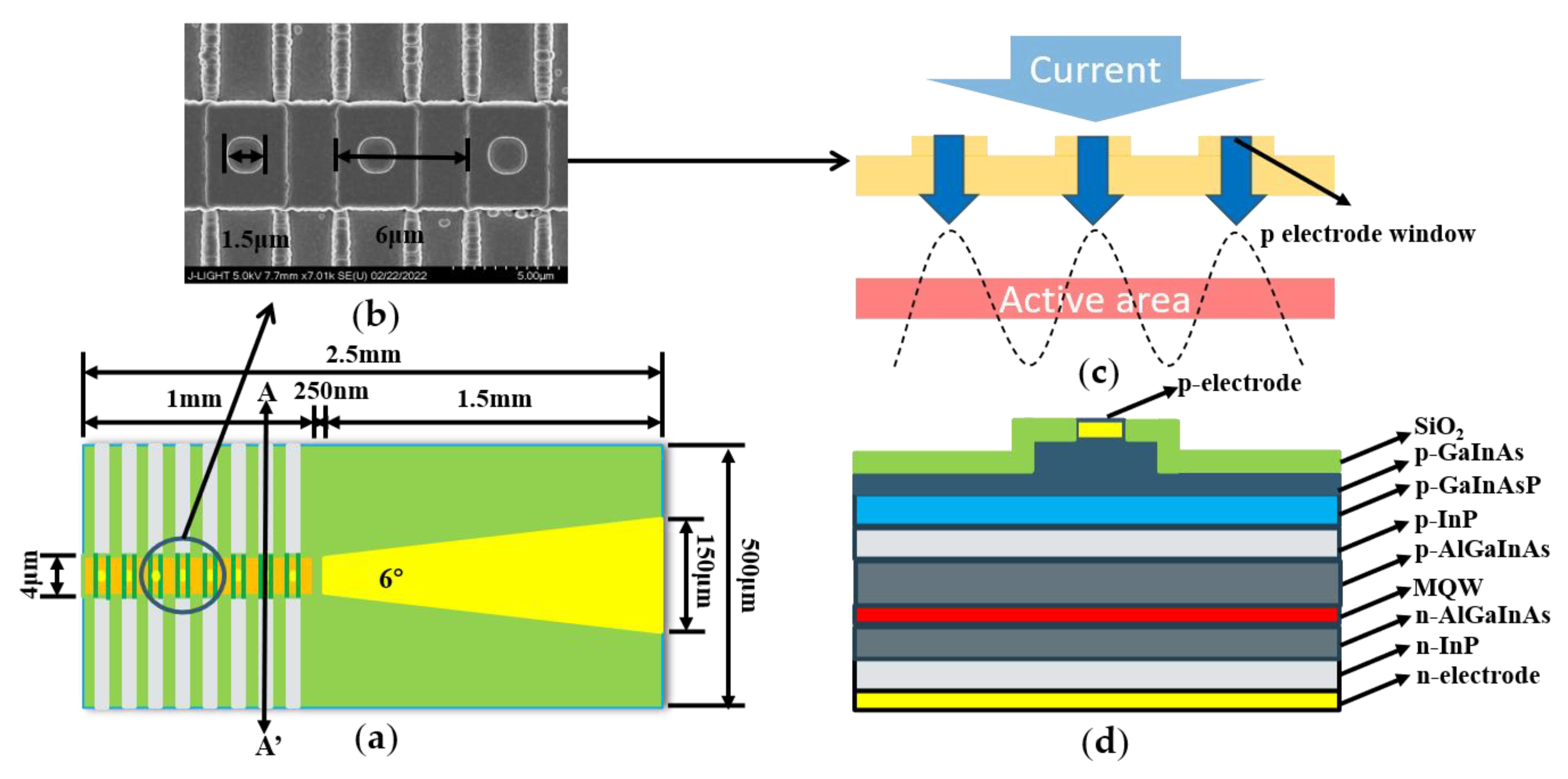
2. Materials and Methods

The device consists of two parts: the front part is the DFB laser, and the rear part is the tapered waveguide as shown in Figure 1a. In the DFB laser section, the period of the grating was 6.0 μm, and the ridge waveguide (W = 4.0 μm, L = 1.0 mm) was in the center of the grating. Electrode windows (R = 1.5 μm) were patterned on the grating to form periodic electrical injection channels, and there was no current injection anywhere except at the electrode windows. The topography of the surface grating and periodic electrodes windows can be seen by scanning electron microscopy (SEM) as shown in Figure 1b. A tapered waveguide (L = 1.5 mm) with a 6° taper angle increased the output power of the device. The width of the tapered waveguide port was 150 μm. The insulating channel between the two parts is 250 nm to ensure that the two parts are independently connected to electricity without affecting each other. Ti/Pt/Au metal layers are deposited as p-and n-electrodes by magnetron sputtering. The lift-off technique is used to define the p-electrode shape. Thermal annealing is then applied to improve metal contact and lower electrical resistance. Then the lasers are obtained after wafer cleaving, and two cleaved facets are coated with silicon oxide layer for anti-reflection and protection. The current that defines the access front part is IDFB, and the rear part is ITap. The device (W = 500 μm, L = 2.5 mm) is soldered to a heat sink with the p-side facing down to form an ohmic contact mounted on a thermoelectric cooling (TEC) controlled stage for temperature tuning. No complex process technology is used in the entire process, which makes the fabrication simple and low-cost.
The surface gratings, ridge waveguides, taper waveguides, and periodic electrodes were all fabricated by i-line lithography, after which inductively coupled plasma (ICP) is used to etch them. The surface grating was fabricated by inductively coupled plasma shallow etching, which helped to reduce scattering loss. The periodic electrical injection creates periodic gain differences in the active area, as can be seen in Figure 1c. Considering that surface gratings cause simultaneous changes in the real and imaginary parts of the refractive index, we have carefully designed them to avoid too many refractive index coupling effects to prevent higher-order scattering, which can cause additional optical losses and increase the threshold. The coupling coefficient κ is expressed as:
κ = k 0 Γ Δ n sin l π Λ L g l π + i Γ Δ g 4
where k 0 = 2 π / λ 0 is the vacuum wave number for the vacuum wavelength λ 0 . Γ is the optical confinement factor of the gating in our device. Δ n is the refractive index change in the waveguide. L g represents the grating’s groove width. Λ is the period for the l order grating ( Λ = l π / n e f f ) and Γ is the optical confinement factor of the active region. Δ g represents the gain/loss change in the waveguide.
By analyzing the coupling coefficient κ , the influence of the refractive index coupling on the device is reduced by decreasing Δ n and Γ in the real part, and increasing Δ g in the imaginary part makes the gain coupling occupy the main modulation position in practical work. It is known by calculation that the imaginary part is 4 orders of magnitude higher than the real part. This means that the strength of the refractive index coupling is negligible, and the device is mainly modulated by the gain coupling. The epitaxial structure of the device was fabricated by metal-organic chemical vapor deposition (MOCVD), as shown in Figure 1d. The active region of the device was made of AlGaInAs material, which reduced the linewidth of the device.
The 3 dB linewidth of the device was tested by the frequency-shifted non-zero delay self-heterodyne method. As shown in Figure 2, the output signal of the DFB laser entered coupler 1 after passing through the isolator and was then split into two paths. One path was delayed by the fiber ring and then sent to coupler 2; the other path was sent to coupler 2 through an acousto-optic modulator (AOM), and the two paths were mixed by the detector. Following this, the difference frequency electrical signal was sent to the spectrum analyzer. The fiber-optic delay line was formed of a 50 km long single-mode fiber. Couplers 1 and 2 were single-input double-output types with a split ratio of 1:1. AOM was an acousto-optic frequency shifter with a frequency up-shift of 80 MHz.

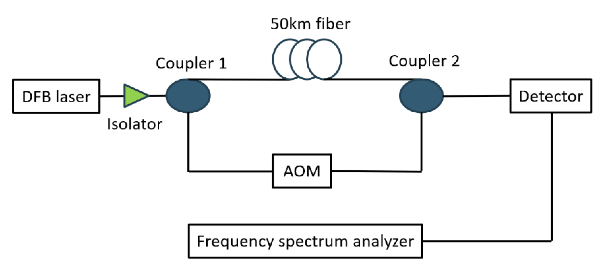
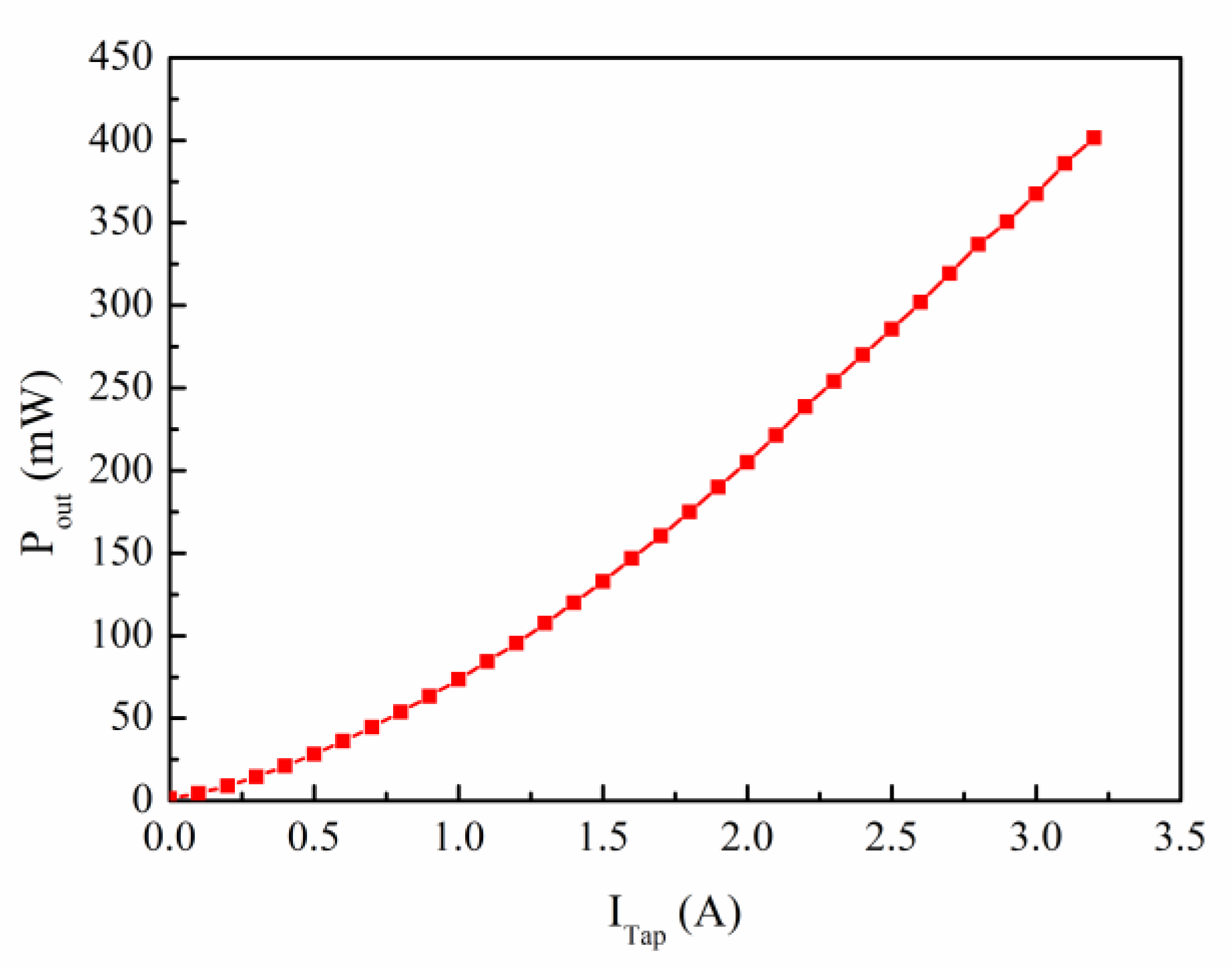
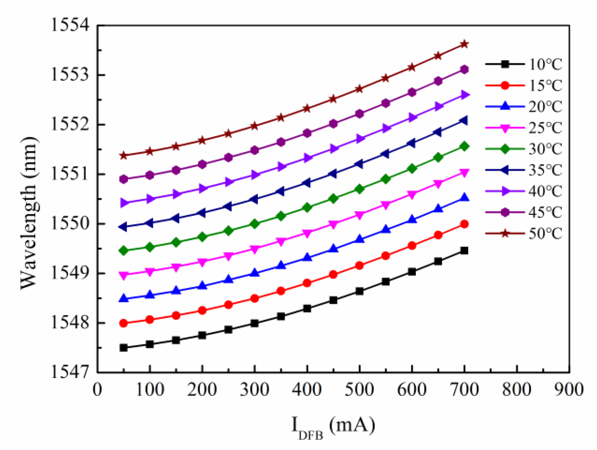
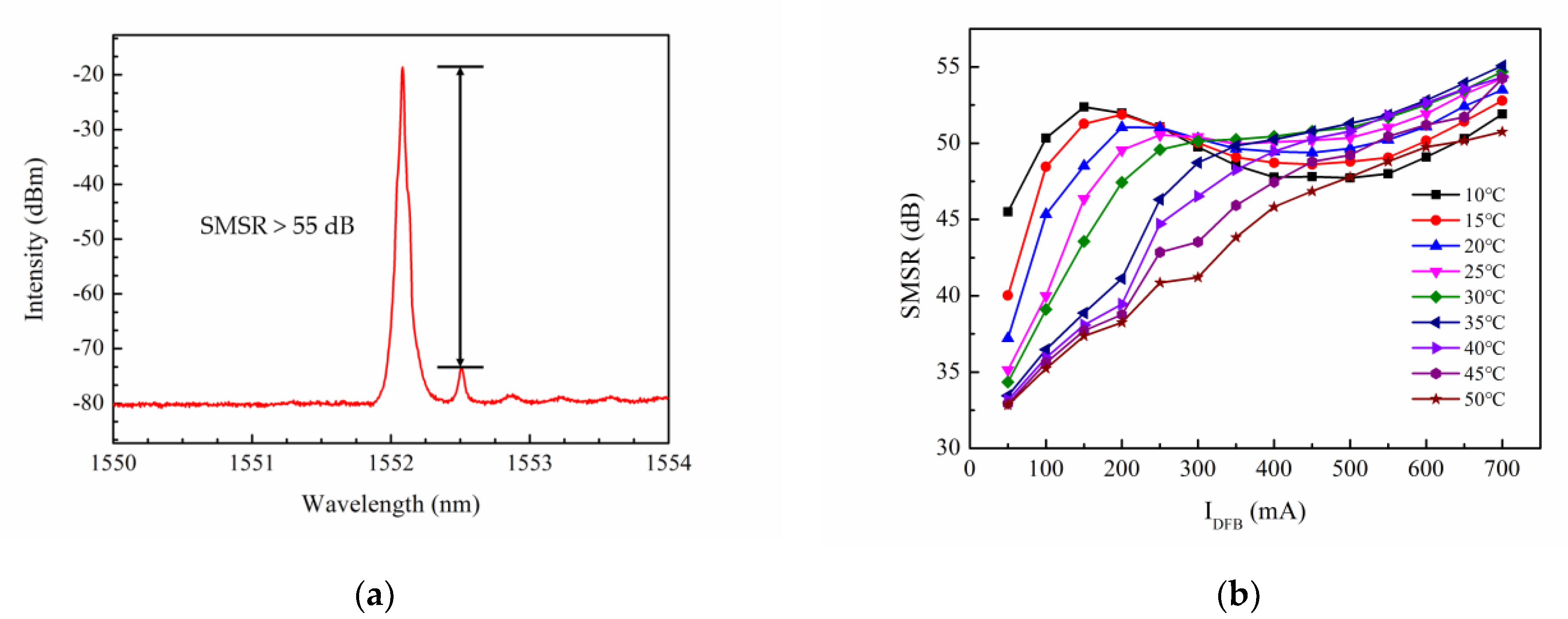
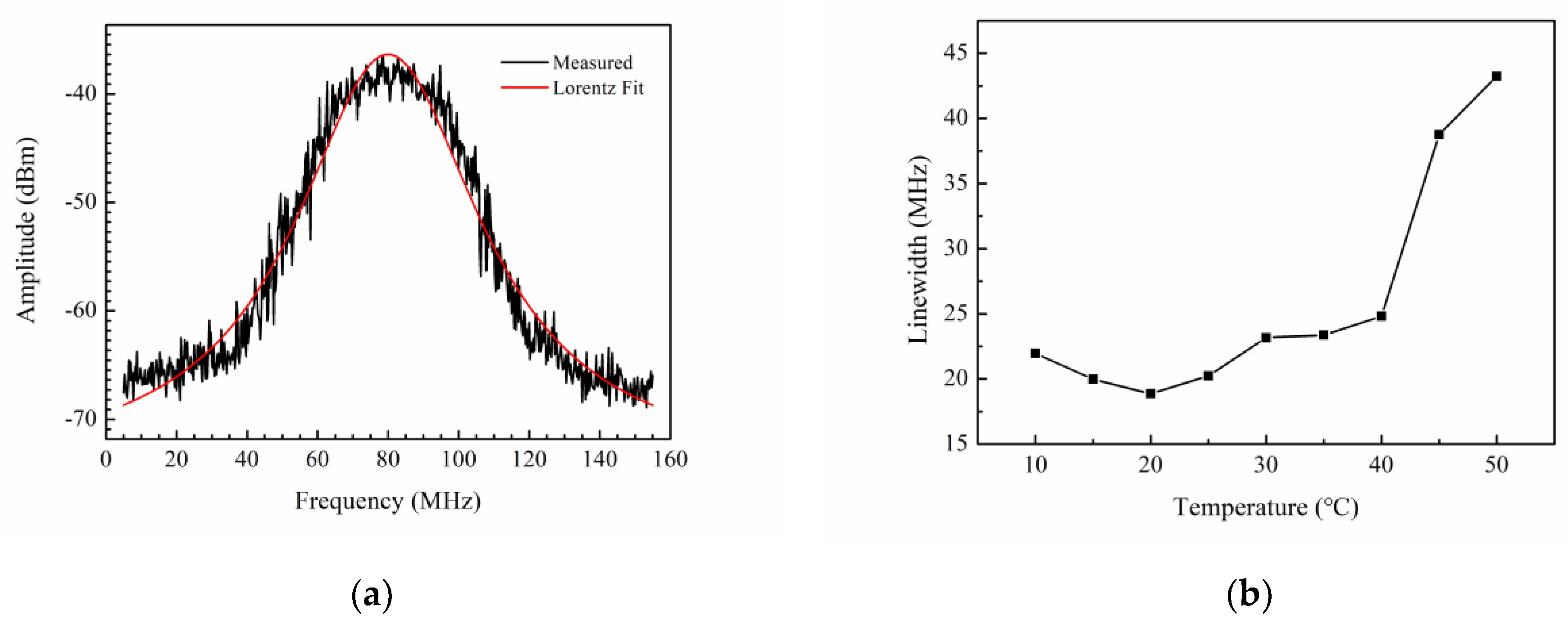
3. Results and Discussion

The power-current (PI) characteristics with CW operation at 20 °C are shown in Figure 3. The threshold current of the DFB laser was measured to be 20 mA. Figure 3 shows that when the IDFB was fixed, an increase in the ITap resulted in increased output power. As the current was increased to 3.0 A, the output power reached 401.5 mW. During this period, the curve maintained a good linear trend and did not reach the non-linear region of saturation, so we hypothesize that the output power will be significantly improved significantly at higher currents.
Figure 4 shows the spectra of different IDFB values (from 50 mA to 700 mA, measured every 50 mA) at a fixed ITap value of 0.5 A at 20 °C (measured with AQ6370C spectrum analyzer with a spectral resolution of 0.02 nm). As the current increased, a significant number of carriers were injected into the device, causing the refractive index of each layer to change. In addition, the injection of carriers caused a build-up of heat in the device, which eventually led to the narrowing of the bandgap of the gain material in the active region. This means that the gain peak and the corresponding lasing wavelength to the long-wavelength cause a red shift. The wavelength redshift of Figure 4 was from 1548.44 nm to 1550.52 nm (2.08 nm). The spectrum shows that several side peaks appeared in addition to the main laser peak as the current increased. Although side peaks also appeared, the SMSRs at all lasing wavelengths were still over 37 dB, indicating that the device always displayed acceptable single-mode operating characteristics.
Figure 5 shows the variation curve of the central lasing wavelength obtained by changing the IDFB at different temperatures. When the temperature was constant, the lasing wavelength increased as the values of IDFB increased. Similarly, as the temperature increased from 10 °C to 50 °C, the lasing wavelength also increased. It can be seen from Figure 5 that the change in lasing wavelength for different current wavelengths at different temperatures is almost linear. This is due to the fact that the surface Bragg grating in the device is minimally affected when the temperature increases. However, the bandgap and refractive index do change in a linear relationship. This also limits the rate of change of the lasing wavelength for the DFB laser with temperature. However, this also makes the single-mode stability of the device excellent, and no mode-hopping phenomenon occurs. The achieved quasi-continuous tuning range is 6.156 nm (from 1547.468 nm to 1553.624 nm), and the rate of change of lasing wavelength with temperature was 0.154 nm/°C.
As shown in Figure 6a, the maximum SMSR of the device exceeded 55 dB. At the same time, the SMSR at different temperatures and different values of IDFB were also measured, which are displayed in Figure 6b. It is clear that when the temperature and the current were lower, and just after the laser had begun lasing, the SMSR increased proportionally with the increase in current. As the IDFB increased slightly, a side mode appeared, causing the side mode and the main mode to compete. This caused the SMSR to become smaller as the IDFB increased. This situation improved as the current continued to increase. This is because, at the high current level, the main mode dominates, which suppresses the increase in the side mode, increasing the size of the SMSR. At high temperatures, the lasing wavelength of the DFB laser will move to a long wavelength. This means that the mode competition will also move to a long wavelength. However, as the performance of the device will decrease at high temperatures, non-radiative recombination will consume more carriers, and the carriers are mainly provided to the lasing mode. This means that the side modes will not receive many carriers, and so the SMSR will increase with the increase in IDFB.
The 3 dB linewidth test results are shown in Figure 7. The measured spectral range was 160 MHz with a resolution of 1 MHz. Figure 7a shows the 3 dB linewidth measured at 20 °C using a delay self-heterodyne linewidth test system. In the spectrogram, the 3 dB linewidth represents the spectral width corresponding to the 3 dB drop from the maximum value of the spectral line amplitude. The measured spectral lines are of the Lorentz line type, so more accurate results can be obtained by performing a Lorentz fit on the measured spectral lines. The measured results have been fitted by the Lorentz method, and the fitted 3 dB linewidth was 18.86 MHz. As the temperature increased, the linewidth generally displayed a clearer trend. In theory, when the output power is not saturated, the linewidth of the semiconductor laser is proportional to the derivative of the output power. However, in practice, the linewidth expands twice due to the linewidth enhancement factor and the spatial hole burning effect. Therefore, the actual measured line width is affected by multiple factors. Increasing the differential gain and optimizing the coupling coefficient had a beneficial impact on reducing the linewidth of the semiconductor laser. The device maintained a stable single longitudinal mode output throughout the test period.
The performance characteristics of the DFB laser fabricated in this study were compared with those of other reported DFB lasers. The results are listed in Table 1. As can be seen from Table 1, all devices do not perform very well on all characteristic parameters. The device fabricated in this paper is much higher than that reported in other literature in terms of output power and can have a high SMSR while maintaining high output power. In terms of tuning range and line width, it is not as excellent as the output power and SMSR performance. In the following research, we will focus on how to improve the tunable range and reduce the linewidth and then make our device more perfect.

4. Conclusions

In this paper, we demonstrated a high-power surface grating 1550 nm tunable DFB laser based on the gain-coupling effect. The gain coupling effect was realized by forming a periodic gain difference with periodic p-electrode windows. A tapered waveguide was introduced to improve the output power, and a multiple quantum well structure formed of AlGaInAs material was used in the active region to reduce the linewidth of the laser. Our device achieved consistently excellent performance. This was exhibited by CW output power of 401.5 mW at 20 °C, a maximum side-mode rejection ratio exceeding 55 dB, a measured 3 dB linewidth was 18.86 MHz, and a wavelength quasi-continuous tuning range of 6.156 nm from 10 °C to 50 °C. Our device does not use complex manufacturing techniques such as secondary epitaxial growth and can be manufactured by i-line lithography, which improves yield and achieves stable working conditions. This provides a low-cost, high-efficiency, high-yield DFB laser for use in the fields of space laser communication, lidar, and laser ranging.

Author Contributions

Conceptualization, L.L. and L.Q.; methodology, Y.L. and Y.C.; software, P.J. and C.Z.; validation, X.L. and L.L.; formal analysis, Y.W., Y.S., H.T., and C.Q.; investigation, P.J., Y.C., Y.W., C.Y., and Y.L.; resources, L.Q. and L.L.; data curation, X.L. and L.L.; writing—original draft preparation, X.L.; writing—review and editing, L.L.; visualization, X.L.; supervision, L.L. and L.Q.; project administration, L.Q.; funding acquisition, L.Q. and L.W. All authors have read and agreed to the published version of the manuscript.

Funding

This work was supported by the National Key R & D Program of China [2021YFF0700500]; the National Natural Science Foundation of China [11874353, 61904179, 62090054, 61934003, 62090052, 62090051]; the Science and Technology Development Project of Jilin Province [202001069GX, 20200501006GX, 20200501007GX, 20200501008GX]; and the Dawn Talent Training Program of CIOMP.

Institutional Review Board Statement

Not applicable.

Informed Consent Statement

Not applicable.

Data Availability Statement

Not applicable.

Acknowledgments

The authors would like to thank Lei Liang, Li Qin, Yuxin Lei, Peng Jia, Hui Tang, Changjin Yang, Yongyi Chen, Yubing Wang, Yue Song, Cheng Qiu, Chuantao Zheng, Lijun Wang for helping with this article.

Conflicts of Interest

The authors declare no conflict of interest.

References

  1. Toyoshima, M.; Takayama, Y.; Takahashi, T.; Suzuki, K.; Kimura, S.; Takizawa, K.; Kuri, T.; Klaus, W.; Toyoda, M.; Kunimori, H.; et al. Ground-to-satellite laser communication experiments. IEEE Aerosp. Electron. Syst. Mag. 2008, 23, 10–18. [Google Scholar] [CrossRef]
  2. Müller, G.J.; Berlien, P.; Scholz, C. The medical laser. Med. Laser Appl. 2006, 21, 99–108. [Google Scholar] [CrossRef]
  3. Schulz, W.; Poprawe, R. Manufacturing with novel high-power diode lasers. IEEE J. Sel. Top. Quantum Electron. 2000, 6, 696–705. [Google Scholar] [CrossRef]
  4. Zhou, Z.; Yin, B.; Michel, J. On-chip light sources for silicon photonics. Light-Sci. Appl. 2015, 4, e358. [Google Scholar] [CrossRef]
  5. Warburton, R.E.; McCarthy, A.; Wallace, A.M.; Hernandez-Marin, S.; Hadfield, R.H.; Nam, S.W.; Buller, G.S. Subcentimeter depth resolution using a single-photon counting time-of-flight laser ranging system at 1550 nm wavelength. Opt. Lett. 2007, 32, 2266–2268. [Google Scholar] [CrossRef]
  6. Strickland, B.R.; Lavan, M.J.; Woodbridge, E.; Chan, V. Effects of fog on the bit-error rate of a free-space laser communication system. Appl. Opt. 1999, 38, 424–431. [Google Scholar] [CrossRef]
  7. Ma, W.; Tan, S.; Wang, K.; Guo, W.; Liu, Y.; Liao, L.; Zhou, L.; Zhou, J.; Li, X.; Liang, L.; et al. Practical two-dimensional beam steering system using an integrated tunable laser and an optical phased array. Appl. Opt. 2020, 59, 9985–9994. [Google Scholar] [CrossRef]
  8. Luo, Y.; Nakano, Y.; Tada, K.; Inoue, T.; Hosomatsu, H.; Iwaoka, H. Purely gain-coupled distributed feedback semiconductor lasers. Appl. Phys. Lett. 1990, 56, 1620–1622. [Google Scholar] [CrossRef]
  9. Kogelnik, H.; Shank, C.V. Coupled-Wave Theory of Distributed Feedback Lasers. J. Appl. Phys. 1972, 43, 2327–2335. [Google Scholar] [CrossRef]
  10. Soda, H.; Kotaki, Y.; Sudo, H.; Ishikawa, H.; Yamakoshi, S.; Imai, H. Stability in single longitudinal mode operation in GaInAsP/InP phase-adjusted DFB lasers. IEEE J. Quantum Electron. 1987, 23, 804–814. [Google Scholar] [CrossRef]
  11. Nilsson, S.; Kjellberg, T. Improved spectral characteristics of MQW-DFB lasers by incorporation of multiple phase-shifts. J. Lightwave Technol. 1995, 13, 434–441. [Google Scholar] [CrossRef]
  12. Orth, A.; Reithmaier, J.P.; Zeh, R.; Doleschel, H.; Forchel, A. First order gain-coupled GaInAs/GaAs distributed feedback laser diodes patterned by focused ion beam implantation. Appl. Phys. Lett. 1996, 69, 1906–1908. [Google Scholar] [CrossRef]
  13. Li, G.P.; Makino, T. Single-mode yield analysis of partly gain-coupled multiquantum-well DFB lasers. IEEE Photonics Technol. Lett. 1993, 5, 1282–1284. [Google Scholar] [CrossRef]
  14. Lowery, A.J.; Novak, D. Enhanced maximum intrinsic modulation bandwidth of complex-coupled DFB semiconductor lasers. Electron. Lett. 1993, 29, 461–463. [Google Scholar] [CrossRef]
  15. Luo, Y.; Nakano, Y. Fabrication and characteristics of gain-coupled distributed feedback semiconductor lasers with a corrugated active layer. IEEE J. Quantum Electron. 1991, 27, 1724–1731. [Google Scholar] [CrossRef]
  16. Okai, M.; Tsuchiya, T. Tunable DFB lasers with ultra-narrow spectral linewidth. Electron. Lett. 1993, 29, 349–351. [Google Scholar] [CrossRef]
  17. Ruan, C.; Chen, Y.; Qin, L.; Ma, D.; Jia, P.; Liu, X.; Liang, L.; Lei, Y.; Zeng, Y.; Song, Y.; et al. Purely gain-coupled distributed feedback Bragg semiconductor laser emitting at 795 nm with a wide tunable range. IEEE Photonics J. 2021, 13, 1500908. [Google Scholar] [CrossRef]
  18. Liu, X.; Chen, Y.; Zeng, Y.; Qin, L.; Lei, L.; Jia, P.; Wu, H.; Ma, D.; Ruan, C.; Ning, Y.; et al. Tunable DFB laser diode based on high-order surface isolation grooves working at 905 nm. Opt. Commun. 2021, 481, 126528. [Google Scholar] [CrossRef]
  19. Lei, Y.-X.; Chen, Y.-Y.; Gao, F.; Ma, D.-Z.; Jia, P.; Cheng, Q.; Wu, H.; Ruan, C.-K.; Liang, L.; Chen, C.; et al. 990 nm High-Power High-Beam-Quality DFB Laser with Narrow Linewidth Controlled by Gain-Coupled Effect. IEEE Photonics J. 2019, 11, 1500609. [Google Scholar] [CrossRef]
  20. Ma, D.Z.; Chen, Y.Y.; Lei, Y.X.; Jia, P.; Gao, F.; Zeng, Y.G.; Liang, L.; Song, Y.; Ruan, C.K.; Liu, X.; et al. 1045 nm purely gain coupled semiconductor laser based on periodic electric injection. J. Lumin. 2020, 225, 117372. [Google Scholar] [CrossRef]
  21. Corbett, B.; Mcdonald, D. Single longitudinal mode ridge waveguide 1.3 μm Fabry-Perot laser by modal perturbation. Electron. Lett. 1995, 31, 2181–2182. [Google Scholar] [CrossRef]
  22. Gao, F.; Qin, L.; Jia, P.; Chen, C.; Cheng, L.; Chen, H.; Liang, L.; Zhang, X.; Chen, Y.; Zeng, Y.; et al. Narrow-Strip Single-Longitudinal-Mode Laser Based on Periodic Anodes Defined by i-Line Lithography. IEEE Photonics J. 2018, 10, 1–10. [Google Scholar] [CrossRef]
  23. Liu, L.; Qu, H.; Wang, Y.; Liu, Y.; Zhang, Y.; Zheng, W. High-brightness single-mode double-tapered laser diodes with laterally coupled high-order surface grating. Opt. Lett. 2014, 39, 3231–3234. [Google Scholar] [CrossRef] [PubMed]
  24. Johannes, T.; Rast, A.; Rieger, J.; Harth, W. Gain-coupled DFB lasers with a titanium surface Bragg grating. Electron. Lett. 2002, 31, 370–371. [Google Scholar] [CrossRef]
  25. Chen, Y.; Jia, P.; Zhang, J.; Qin, L.; Chen, H.; Gao, F.; Zhang, X.; Shan, X.; Ning, Y.; Wang, L. Gain-coupled distributed feedback laser based on periodic surface anode canals. Appl. Opt. 2015, 54, 8863–8866. [Google Scholar] [CrossRef]
  26. Gao, F.; Qin, L.; Chen, Y.; Jia, P.; Chen, C.; Cheng, L.; Chen, H.; Liang, L.; Zeng, Y.; Zhang, X.; et al. Study of gain-coupled distributed feedback laser based on high order surface gain-coupled gratings. Opt. Commun. 2018, 410, 936–994. [Google Scholar] [CrossRef]
  27. Henry, C. Theory of the linewidth of semiconductor lasers. IEEE J. Quantum Electron. 1982, 18, 259–264. [Google Scholar] [CrossRef]
  28. Davies, S.C.; Whitbread, N.D.; Ward, A.J.; Arnold, M.; Griffin, R.A.; Wale, M.J. Reduced Lorentzian linewidth for monolithic widely tunable C-band lasers utilising InGaAlAs/InP active region. In Proceedings of the 2011 Conference on Lasers and Electro-Optics Europe and 12th European Quantum Electronics Conference (CLEO EUROPE/EQEC), Munich, Germany, 22–26 May 2011; IEEE: Piscataway, NJ, USA, 2011. [Google Scholar]
  29. Zhao, Y.G.; Nikolov, A.; Dutt, R. 1550 nm DFB semiconductor lasers with high power and low noise. Proc. SPIE—Int. Soc. Opt. Eng. 2011, 7933, 838–839. [Google Scholar]
  30. Chen, Q.; Jiang, C.; Wang, K.; Zhang, M.; Ma, X.; Liu, Y.; Lu, Q.; Guo, W. Narrow-linewidth thermally tuned multi-channel interference widely tunable semiconductor laser with thermal tuning power below 50 mW. Photonics Res. 2020, 8, 47–52. [Google Scholar] [CrossRef]
  31. Li, X.; Liang, L.; Wang, L.J.; Qin, L.; Chen, Y.Y.; Wang, Y.B.; Song, Y.; Lei, Y.X.; Jia, P.; Zeng, Y.G.; et al. Monolithic Integrated Semiconductor Optical Amplifier with Broad Spectrum, High Power, and Small Linewidth Expansion. IEEE Access 2021, 9, 98863–98873. [Google Scholar] [CrossRef]
  32. Hou, L.; Haji, M.; Akbar, J.; Marsh, J.H. Narrow linewidth laterally coupled 1.55μm AlGaInAs/InP distributed feedback lasers integrated with a curved tapered semiconductor optical amplifier. Opt. Lett. 2012, 37, 4525–4527. [Google Scholar] [CrossRef] [PubMed]
  33. Shi, Y.; Chen, X.; Zhou, Y.; Li, S.; Lu, L.; Liu, R.; Feng, Y. Experimental demonstration of eight-wavelength distributed feedback semiconductor laser array using equivalent phase shift. Opt. Lett. 2012, 37, 3315–3317. [Google Scholar] [CrossRef] [PubMed]
  34. Shi, Y.; Li, S.; Li, L.; Guo, R.; Zhang, T.; Rui, L.; Li, W.; Lu, L.; Song, T.; Zhou, Y.; et al. Study of the Multiwavelength DFB Semiconductor Laser Array Based on the Reconstruction-Equivalent-Chirp Technique. J. Lightwave Technol. 2013, 31, 3243–3250. [Google Scholar] [CrossRef]
  35. Dridi, K.; Benhsaien, A.; Zhang, J.; Hinzer, K.; Hall, T.J. Narrow linewidth two-electrode 1560 nm laterally coupled distributed feedback lasers with third-order surface etched gratings. Opt. Express 2014, 22, 19087–19097. [Google Scholar] [CrossRef] [PubMed]
  36. Dridi, K.; Benhsaien, A.; Zhang, J.; Hall, T.J. Narrow Linewidth 1550 nm Corrugated Ridge Waveguide DFB Lasers. Photonics Technol. Lett. IEEE 2014, 26, 1192–1195. [Google Scholar] [CrossRef]
  37. Li, L.; Tang, S.; Huang, L.; Zhang, T.; Li, S.; Shi, Y.; Chen, X. Experimental demonstration of a low-cost tunable semiconductor DFB laser for access networks. Semicond. Sci. Technol. 2014, 29, 95002. [Google Scholar] [CrossRef]
  38. Lu, J.; Liu, S.; Tang, Q.; Xu, H.; Chen, Y.; Chen, X. Multi-wavelength distributed feedback laser array with very high wavelength-spacing precision. Opt. Lett. 2015, 40, 5136–5139. [Google Scholar] [CrossRef]
  39. Tang, S.; Lu, J.; Li, L.; Xu, H.; Tang, Q.; Chen, X. A Matrix-Grating Equivalent Phase Shifted Laser Array With 25-nm Wavelength Tuning Range. Photonics Technol. Lett. IEEE 2015, 27, 530–533. [Google Scholar] [CrossRef]
  40. Zhao, Y.; Shi, Y.; Li, J.; Liu, S.; Xiao, R.; Li, L.; Lu, J.; Chen, X. A Cascaded Tunable DFB Semiconductor Laser With Compact Structure. IEEE J. Quantum Electron. 2018, 54, 2200111. [Google Scholar] [CrossRef]
  41. Su, Z.; Xiao, R.; Sun, Z.; Yang, Z.; Du, Y.; Chen, Z.; Zheng, J.; Zhang, Y.; Lu, J.; Shi, Y.; et al. 48 channels 100-GHz tunable laser by integrating 16 DFB lasers with high wavelength-spacing uniformity. arXiv 2020, arXiv:2001.01178. [Google Scholar]
  42. Sun, Z.; Xiao, R.; Su, Z.; Liu, K.; Hu, Z.; Dai, P.; Lu, J.; Zheng, J.; Zhang, Y.; Shi, Y.; et al. High Single-Mode Stability Tunable In-Series Laser Array With High Wavelength-spacing Uniformity. J. Lightwave Technol. 2020, 38, 6038–6046. [Google Scholar] [CrossRef]
  43. Sun, Z.; Xiao, R.; Su, Z.; Liu, K.; Lv, G.; Xu, K.; Fang, T.; Shi, Y.; Chiu, Y.-J.; Chen, X. Experimental Demonstration of Wavelength-tunable In-series DFB Laser Array with 100-GHz Spacing. IEEE J. Sel. Top. Quantum Electron. 2021, 28, 1500308. [Google Scholar] [CrossRef]
Figure 1. (a) Overview of the device; (b) SEM schematic diagram of grating and p-electrode window; (c) schematic diagram of carrier distribution for periodic electrical injection; (d) schematic cross-sectional view at AA’ of the overview of the device.
Applsci 12 04498 g001
Figure 2. Delayed self-heterodyne linewidth test system.
Applsci 12 04498 g002
Figure 3. Measured output power with IDFB = 700 mA as a function of ITap.
Applsci 12 04498 g003
Figure 4. Measured spectrum under different IDFB values where ITap = 0.5 A.
Applsci 12 04498 g004
Figure 5. Measured lasing wavelength under different values of IDFB at different temperatures.
Applsci 12 04498 g005
Figure 6. (a) SMSR of the device with IDFB = 700 mA at 20 °C; (b) SMSR at different temperatures and IDFB.
Applsci 12 04498 g006
Figure 7. (a) 3 dB linewidth measurement result at 20 °C; (b) 3 dB linewidth measurement results at different temperatures.
Applsci 12 04498 g007
Table 1. The parameters of the device in this paper are compared with other reported DFB lasers.
YearPoutTunable RangeSMSRLinewidth
2012 [32]210 mW->45 dB64 kHz (3 dB)
2012 [33]>15 mW>15 nm>40 dB-
2013 [34]>13 mW5.88 nm>45 dB-
2014 [35]6 mW3.37 nm>52 dB<170 kHz (3 dB)
2014 [36]7 mW<4 nm>50 dB<185 kHz (3 dB)
2014 [37]>3 mW9 nm>42 dB1.67 MHz (3 dB)
2015 [38]>4 mW30 nm>40 dB-
2015 [39]>1.5 mW25 nm>40 dB-
2018 [40]>15 mW>9 nm>35 dB-
2020 [41]>4 mW40 nm>45 dB0.68 nm (20 dB)
2020 [42]>25 mW10 nm>60 dB-
2021 [43]>10 mW>3.5 nm>55 dB-
This paper400 mW6.156 nm>55 dB18.86 MHz (3 dB)
Publisher’s Note: MDPI stays neutral with regard to jurisdictional claims in published maps and institutional affiliations.

