Article

Application-Specific Integrated Circuit of an Inter-IC Sound Digital Filter for Audio Systems

by
Rene Davila-Velarde
,
Ricardo Ramos-Contreras
,
Luis Pizano-Escalante
,
Omar Longoria-Gandara
* and
Cuauhtémoc Aguilera-Galicia
Department of Electronics, Systems and IT, ITESO, Tlaquepaque 45604, JAL, Mexico
*
Author to whom correspondence should be addressed.
Appl. Sci. 2023, 13(14), 8182; https://doi.org/10.3390/app13148182
Submission received: 17 June 2023 / Revised: 8 July 2023 / Accepted: 11 July 2023 / Published: 14 July 2023
(This article belongs to the Section Electrical, Electronics and Communications Engineering)

Abstract

:
In digital audio systems, filters and equalizers are essential modules for audio improvement at the input and output stages. Due to their computational complexity, most audio tasks are processed with digital signal processors. Due to the fact that latency in audio systems is a critical specification and audio trends require higher sample rates, noise canceling, and bigger data sizes, having an independent high-resolution equalizer would reduce the computational power needed for audio systems. This research had the goal of designing and implementing a hardware architecture for a configurable filter bank based on finite impulse response (FIR) filters and a noise-cancellation stage with an inter-integrated circuit (I2C) communication interface, which allows the filter configuration. The system was implemented as a standalone integrated circuit (IC) for which its inputs were the inter-IC sound (I2S) bus control signals. The digital audio system was optimized to perform one-cycle convolutional operations by implementing a vector–vector arithmetic logic unit. Furthermore, this applied research provides the register transfer level description and the functional verification of the digital design, the system-on-chip (SoC) implementation in TSMC 180 nm technology, and the post-silicon validation with a printed circuit board for testing the output digital signals of the system.

1. Introduction

Filters and equalizers are essential blocks of audio systems, both in their input and output stages [1]. For example, most modern cars are equipped with discrete audio equalizers in order to enable the user to configure the audible sound output with the audio parameters of preference. Usually, in digital audio systems, the main problem is the computational complexity and the latency; for these reasons, the signal processing is handled by digital signal processors, which have better performance than general-purpose processors and an ad hoc digital hardware architecture, but they are very expensive devices. This problem is accentuated by the growth of streaming services and the need to enhance audible sound quality.
With this in mind, by offloading these essential audio-processing tasks to an application-specific integrated circuit (ASIC), the system is able to streamline processes and redirect resources to other critical tasks. Furthermore, from the digital design perspective, it is possible to downgrade the employed microcontroller, which results in a reduction of the overall cost of the audio system.
This applied research proposes a hardware implementation of a filter processing unit (FPU) based on a filter bank integrated with an audio equalizer with a finite impulse response (FIR) and an adaptive filter, which can be used as a noise canceler working with the well-known least-mean-squares (LMS) and normalized least-mean-squares (NLMS) algorithms. Given that the core element of these algorithms is an FIR filter, small modifications such as a predefined filter coefficient bank and a user-defined filter were added to deliver a full audio system, which consists of a configurable high-resolution equalizer and a noise canceler compliant with a left-justified inter-IC sound (I2S) bus and controlled through an inter-integrated circuit (I2C) bus. The system-on-chip (SoC) prototyping approach was implemented on field-programmable gate array (FPGA) technology and the physical ASIC in TSMC 180 nm technology.
The paper is organized as follows. Section 2 gives an overview of the implemented noise-canceling algorithms and describes the proposed architecture for the digital filtering. Section 3 shows the results of the SoC implementation on FPGA technology and the manufactured ASIC with the resulting layout. This section also provides the post-silicon validation and presents the printed circuit board (PCB), which enables the ASIC and the test environment; finally, a discussion of the results is provided. Section 4 draws some conclusions.

2. Materials and Methods

2.1. Noise-Cancellation Algorithms

Noise control is the process of reducing the adverse effects of acoustic noise with the purpose of improving the quality of human life in a determined environment or the user experience with audio devices. The noise control methods are divided into passive and active methods. Conventional passive noise control (PNC) utilizes absorbers and mufflers, but those provide degraded performance at low frequencies of acoustic noise. Relevant applied research has been performed in active noise schemes, such as [2], where active noise reduction was applied to diesel engines by using an adaptive algorithm with an artificial intelligence strategy. Another research proposal [3] was applied in the automotive industry, where the interest was to have low-noise vehicles. This work proposes an active noise reduction based on the analysis of the tire pattern noise. Therefore, active noise control (ANC) methods are mostly used at low frequencies. ANC is based on the principle of the destructive interference of the unwanted noise [4]. The least-mean-squares (LMS) algorithm is the most-popular adaptive algorithm because of its simplicity and robustness [5]; the objective of the algorithm is to generate an adaptive filter, whose coefficients are continuously modified in a way that the unwanted noise is removed from the audio signal [2]. An ordinary least-squares regression powered with a stochastic gradient descent method [6] estimates the error at the current time, and the new filter values are calculated in each iteration, given by
w ( n + 1 ) = w ( n ) + μ x ( n ) [ e ( n ) ] *
where w stands for the filter coefficient vector, x the input signal vector, e the error, defined as the difference between the objective and actual output, μ a sensitivity constant to control the convergence rate of the filter, and finally, n the number of the current input sample. The asterisk denotes complex conjugation. The control system is, thus, updated with each new sample acquired.
The NLMS algorithm [7] solves the convergence problem of the traditional LMS, where, due to the unknown nature of the input signal, an appropriate value for the learning rate μ is difficult to choose. This is solved by normalizing the input signal and reducing the sensibility factor of the input signal power. The new filter values for each iteration are obtained by
w N ( n + 1 ) = w N ( n ) + μ x ( n ) [ e ( n ) ] * | | x ( n ) | | 2 + β
where | | x ( n ) | | refers to the magnitude of the input signal vector and β is a sensitivity constant used to prevent the function from reaching an indeterminate value when the input signal power’s limit approaches zero, and setting a large β if needed, the change in the filter’s new coefficients will not peak.

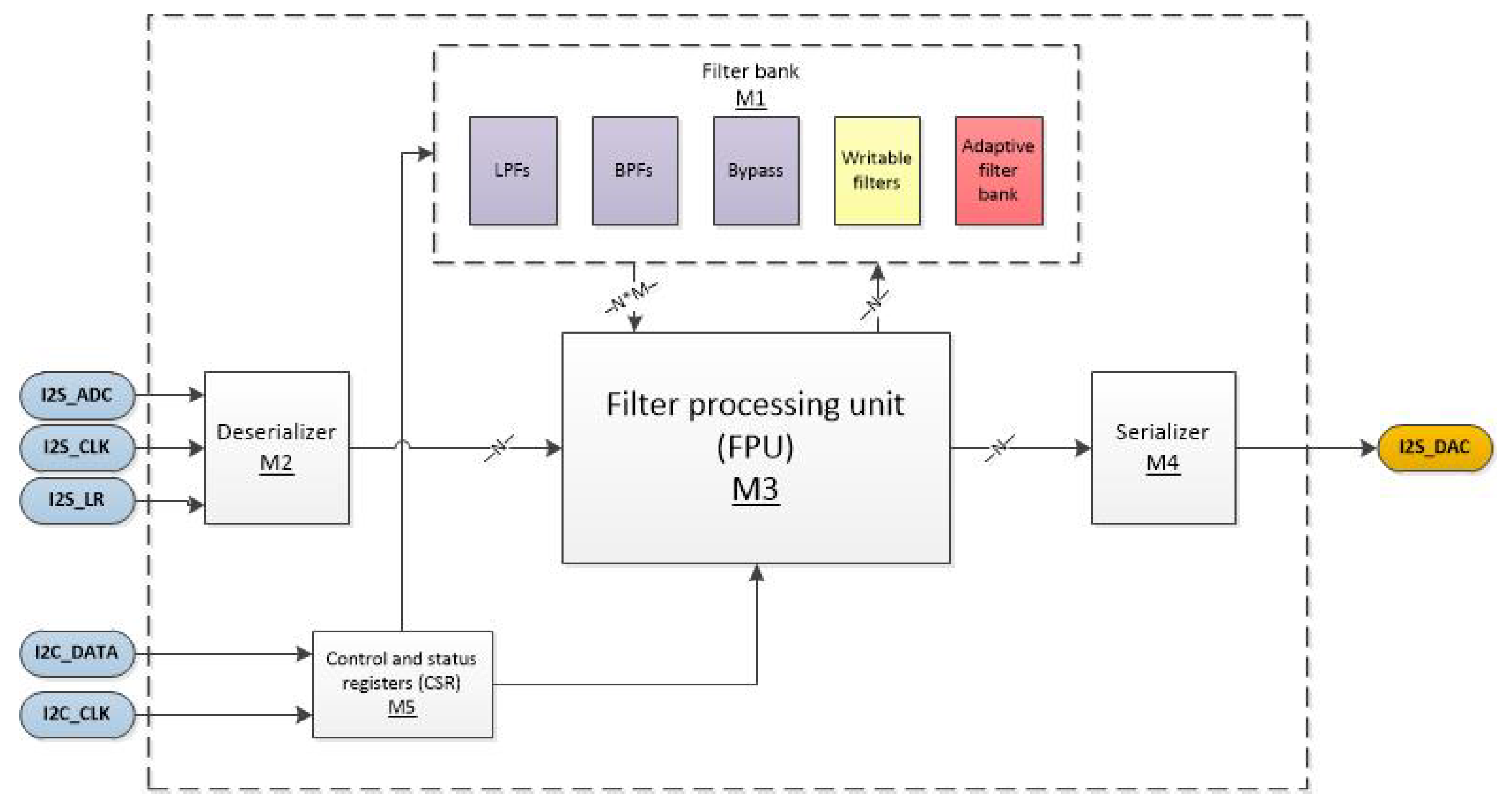
2.2. Digital Filter Architecture

There are multiple recommended FIR architectures in the open literature [8], and some of them are intended to minimize the hardware complexity of FIR filters for applications with constrained resources [9]. This section describes the hardware architecture and design considerations of the digital filter module, as shown in Figure 1.
The word length of the input, the output, the filter coefficients, and the filter order were fixed to K + 1 = 16 , because the flow control is deeply attached to the audio codec (the device that encodes analog audio as digital signals and decodes digital back to analog) word length.
Using the word length of K + 1 = 16 bits (including the sign bit) and assuming the considerations described in Appendix 1 of [9], the signal-to-quantization-noise-power ratio ( S Q N R ) in decibels is given by:
S Q N R = 10 log 10 ( 2 K 2 ) 2 ( 1 / 12 )
which corresponds to the typical value for high-definition audio.
Table 1 describes the type and functionality of all the filtering module signals. The ASIC can be seen as an I2S filtering unit. The module receives a 16-bit serial stereo input and should output a signal with the same format; therefore, there is a deserializer (M2) saving the serial input in the inner registers, and the input values in said registers will be filtered (M3) based on the selected filters from the filter bank (M1), which can be written through an independent I2C interface (M5); finally, the output values will go through a deserializer (M4), returning it to its original format. Both I2S_ADC and I2S_DAC, input and output, respectively, will share the same control signals, I2S_CLK and I2S_LR. The output is synced with its corresponding LR input; the timing and input–output delay based on each filter mode can be seen in Figures 5 and 6.

2.2.1. Filter Bank (M1)

The filter coefficients were obtained by the window method for an FIR filter. For more information about the generation of the coefficients, refer to the Python library, Scipy-Signal firwin. Table 2 shows the cutoff frequencies of the predefined filters.
The filter bank can be bypassed if the bypass mode is selected. The configurable filters consist of two user-writable filters using the I2C bus. The adaptive filter bank is a single 16-order filter, which can only be written by the system itself when using the adaptive filtering mode.

2.2.2. Deserializer (M2)

The deserializer module converts the input serial data into a 16-bit word. Figure 2 shows the block diagram consisting of a shift register with 16 D-type flip-flops.

2.2.3. FPU (M3)

Figure 3 shows the signal processing data path for a deterministic mono filter. Once the data are deserialized to a 16-bit word, they enter the first stage, which consists of a 16-stage shift register, and the previous data move forward in the register chain when there is a positive edge from the left–right data selector.
When the left–right data selector is low, a single step of the convolution between the input data in the shift register and the filter bank coefficient is performed in the multiply–accumulate (MAC) unit. This filtered signal, after 16 clock edges, will be again serialized in the next stage. Figure 4 describes the complete stereo filtering diagram constructed with two mono filtering modules, where the right and left channels are multiplexed based on the value of the I2S LR signal. It is important to note that, with these features, the stereo filtering module is I2S-compliant.

2.2.4. Serializer (M4)

The serializer module converts a 16-bit word to subsequent pulses having the I2S clock as a reference. The output is the overall output of the system, corresponding to the I2S_DAC signal.

2.2.5. Control and Status Register (M5)

The control and status register (CSR) module controls the audio codec configuration through the I2C bus. This module receives and stores the filter coefficients and the configuration parameters for the main control register (MCR). Table 3 shows the memory map of the CSR, where the address 0h0 to 0h1 contains the configuration bits of the MCR and the slave address of the audio codec; the address 0h2 to 0h5 contains the sensitivity parameters of the adaptive filter, and address 0h6 to 0h45 contains the user-defined filter coefficients stored in 16 bits (high and low bytes).

Main Control Register

The MCR controls the main output configuration options and operation modes based on the value of the eight bits described in Table 4. The output control (OUTC) bits allow four operation modes, as described in Table 5, set to 0h1 by default (bypass mode).
The filtering options (FOPTs), Table 6, configure the filter to be used when the OUTC register is configured as filter output mode (0h2), set to 0h0 by default (LPF0).
The adaptive filter mode (AFM) described in Table 7 allows the selection of the algorithm that will be used for the adaptive filtering.

I2C

The register shown in Table 8 configures the slave address for the I2C module. This register is set to 0 × 45 by default.

Sensitivity Numerator Constant Register and Sensitivity Denominator Constant Register

The sensitivity numerator constant (SNC) register in Table 9 sets the LMS and NLMS sensitivity numerator constant ( μ constant). This register is set to 0x3FFF by default (0.499969482421875 in Q1.15 fixed-point format).
The sensitivity denominator constant (SDC) register in Table 10 sets the NLMS sensitivity numerator constant ( β constant). This constant is ignored when the LMS algorithm is selected. This register is set to 0 × 4000 by default (0.5 in Q1.15 fixed-point format).

User-Defined Filters

Table 11 describes the user-defined filter 0 (UDF0) registers, which represent the first writable filter coefficients of the system. These registers are set to 0h0 by default.
Table 12 describes the UDF1 registers, which represent the second writable filter coefficients of the system. These registers are set to 0h0 by default.

2.2.6. Process Timing

Figure 5 and Figure 6 show the user-defined/adaptive filtering processes’ timing, respectively. The top signals can be found in both deterministic FIR filtering and adaptive filtering; I2S_CLK and I2S_LR are the main control signals, where I2S_CLK is the general clock signal and I2S_LR is the left–right synchronization signal; if high, the left channel data are provided by the ADC and the output DAC taken by the DAC, whilst the low state selects the right channel.
The subsequent highlighted values represent the processes needed for both FIR user-defined and adaptive filtering, respectively. The nomenclature used in the diagrams to differentiate left from right channel processing over time is given by: [channel][number of data]. The channel can be either L (for the left channel) or R (for the right channel). The number of data starts at zero, representing the beginning of the data frame and the increments per each positive edge of the I2S_LR, which indicates the start of the next data for both channels. For example, if an L3 is in the deserialization row, it means that the third left data will be processed by the deserialization module for 16 I2S_CLK cycles or half a cycle from I2S_LR in the time given by the column intersection.
Table 13 describes the different stages required to process the input signal with the selected filtering, i.e., user-defined or adaptive filtering.

3. Implementation Results and Discussion

3.1. FPGA Implementation

The design was implemented in the Verilog hardware description language with Intel FPGA technology. The register transfer level (RTL) architecture in Verilog of every module, the functional verification, the timing diagrams, and additional material are described in [10]. Figure 7 corresponds to the Intel-Quartus fitter report, which shows the summary of the required logic elements, registers, multipliers, and pins that form the project, with a specific FPGA.
The Cyclone IV FPGA used to emulate the hardware had enough resources for this specific design using only 3% of the total logic elements, 2% of the total embedded multipliers, and no memory bits; instead, the entire design can be achieved by using only registers. Although the entire project can be developed with only 10 multipliers, these are the most-area-consuming cells in the entire project, and this is a critical parameter for the physical implementation. The information shown in Figure 8 was used in the VLSI implementation as the timing requirements; the maximum input frequency, considering 44.1 kHz as the sample rate with a 16-bit stereo input, was 1.4112 MHz; this timing analysis ensured that every critical path can be synthesized.
The functional validation of the digital audio system prototyped in FPGA technology was carried out with a development platform based on a Cyclone IV FPGA (Terasic DE1) with a Signal Tap embedded logic analyzer. The audio digital signal coming from the I2S was tested with each one of the filter operation modes defined by the FOPT, as was described previously in Table 6. For a more-detailed description and validation of each individual module, refer to [10].

3.2. Physical Implementation

The designed Verilog model was logically synthesized using TSMC 180 nm technology and the Genus tool from Cadence. The resulting netlist based on standard cells of such technology was verified with the Conformal tool to check the logic equivalence of both models. After checking the functionality and timing of our design, the physical chip design was performed by adding to the chip core the I/O pads, the power grid, the clock tree, the floor plan, the place and route of the chip, and physical verifications. This workflow was achieved with the Innovus tool, also from Cadence.
The abstract physical design was exported to the Virtuoso tool to carry out the final verifications such as layout versus schematic (LVS) and design rule checking (DRC). Furthermore, the graphic design system (GDS) file was generated with Virtuoso to send this file to the foundry. The chip physical design and the floor plan of the design modules are shown in Figure 9a,b, respectively.
The pinout of the chip was as follows: serialIn, clk, rst, SDA, sideSelector, serialOut, SCL, vdd, vss (core power supply, 1.8 V), dvdd, and dvss (3.3V I/O power supply). In order to handle more than the required current for the core and to close the pad ring, extra vdd, vss, dvdd, and dvss pads were added to the remaining pins of the dual in-line (DIP) 28 package. The ASIC implementation shown in Figure 10 was manufactured by EUROPRACTICE IC Service using TSMC’s 180 nm CMOS technology.

3.3. Validation and Testing

A PCB was designed in order to supply power to the package, connect to the I2S and I2C buses, and test the ASIC in an environment close to its real-world application. The test environment shown in Figure 11 consisted of:
  • I2C master to select the working filter;
  • I2S master to provide sound data;
  • I2S slave to read the data after filtering;
  • Logic analyzer to debug serial protocols.
With the purpose of capturing the response of the different FIR filters available in the ASIC, a chirp signal was generated and sent through the I2S to the PCB input pins using the I2S master. After capturing the output using the I2S slave, the power spectral density for each filter output mode was obtained with Matlab, as shown in Figure 12.
The filter bank considered four types of filters: There were two low-pass filters with an equivalent cut-off frequency of 1.894 kHz and 3.875 kHz; these filters were intended for low-/low–mid-frequency filtering. There were two band-pass filters of 1.033 kHz–19.035 kHz and 4.478 kHz–9.474 kHz; these filters were intended for mid-/mid–high-frequency filtering. It can be observed that the true cut-off frequencies had a slight deviation from the theoretical design. Finally, the testing of the adaptive filter was approached by using a spectral density estimation of the recorded data.

3.4. Discussion

The main core of the project consisted of a one-cycle vector-to-vector MAC unit generating an FIR filtering hardware unit; there are more refined hardware architectures that are not combinational logic circuits that would help to shorten the biggest critical path in the design, i.e., the FPU; however, this improvement cannot be implemented since the design relied on the I2S bus clock. For this reason, it is important for further implementations to improve the MAC unit to a sequential logic scheme while being able to increase the system clock. Although this is an audio-related ASIC, it is not an analog audio device; therefore, the parameters of the insertion loss, gain, total harmonic distortion, and other audio-related specifications do not apply; these parameters will be defined by the power amplifier, which this module will be connected to.
According to the SQNR, defined previously, and from the measured results, it is clear that having a wider word length, and consequently a higher filter order, will improve the SQNR and produce a sharper filter response.
Due to the complexity of setting the hyperparameters of the adaptive filter μ and β , testing in different environments and rapidly changing its configuration to find one that fit these environments the best were cumbersome. We believe that these can be circumvented by adding a layer on top of this, which incorporates a Gaussian process and Bayesian optimization [11], algorithms used widely in active noise-cancellation applications.

4. Conclusions

Due to the fact that audio applications have high demand in different sectors of information technology, such as the IoT and streaming, it is mandatory to provide good audio quality to the users. In this scenario, ASIC implementations of digital filters are a resourceful option for audio systems with standard configuration protocols such as SPI and I2C. For this reason, the ASIC implemented in this work provides an important alternative to audio signal processing in hardware instead of the typical software approach for noise canceling.
Because of the high cost due to ASIC manufacturing, the FPGA prototype implementation of the proposed equalizer was a very useful stage in the ASIC implementation as a proof of concept and a reference model for the ASIC’s functionality validation. With this design flow, the importance of prototyping before ASIC manufacturing was confirmed.
It is worth mentioning that the TMSC 180 nm testing technology used to manufacture the ASIC can be changed for commercial leading-edge nanometric technologies, but taking advantage of the same digital system design.
During the FPGA implementation phase of the proposal, we found that the adaptive filter was able to reduce or eliminate static noise (crackling sound), but not white noise at low SNR values; to avoid this problem, the word length of the filter coefficients was increased, and an overflow–underflow condition was added to the design. Consequently, the system performance had an audible quality improvement. These changes imply that the format and the word length of the filter coefficients improve the signal-to-noise quantization ratio upon further developments. Following the input word convention of matching the word length with the filter order and as this ASIC is intended to be used in conjunction with an I2S bus, the highest audio sampling standard to be used is a 24-bit stereo word.

Author Contributions

Conceptualization, L.P.-E.; Software, C.A.-G.; Investigation, R.D.-V. and R.R.-C.; Project administration, O.L.-G. All authors have read and agreed to the published version of the manuscript.

Funding

This research received no external funding.

Institutional Review Board Statement

Not applicable.

Informed Consent Statement

Not applicable.

Data Availability Statement

Not applicable.

Conflicts of Interest

The authors declare no conflict of interest.

Abbreviations

The following abbreviations are used in this manuscript:
AFMAdaptive filter mode
BPFBand-pass filter
CLKCLK
CSChannel side
DRCDesign rules check
DSPDigital signal processor
EQEqualizer
FIRFinite impulse response
FOPTFilter option
FPGAField-programmable gate array
ICIntegrated circuit
IOInput–output
I2CInter-integrated circuits
I2SInter-IC sound
LECLogical equivalence checking
LMSLeast mean square
LPFLow-pass filter
LRLeft–right
LSBLeast-significant bit
MACMultiply–accumulate
MCRMain control register
MSBMost-significant bit
MUXMultiplexer
NLMSNormalized least mean square
NUNot used
OUTCOutput configuration
RAMRandom access memory
ROMRead-only memory
rstReset
RTLRegister transfer level
SDCSensitivity denominator constant
SNCSensitivity numerator constant
UDFUser-defined filter
VLSIVery-large-scale integration

References

  1. Pepe, G.; Gabrielli, L.; Squartini, S.; Cattani, L. Designing Audio Equalization Filters by Deep Neural Networks. Appl. Sci. 2020, 10, 2483. [Google Scholar] [CrossRef] [Green Version]
  2. Kwon, S.; Kim, B.-S.; Park, J. Active Noise Reduction with Filtered Least-Mean-Square Algorithm Improved by Long Short-Term Memory Models for Radiation Noise of Diesel Engine. Appl. Sci. 2022, 12, 10248. [Google Scholar] [CrossRef]
  3. Lee, S.-K.; An, K.; Cho, H.-Y.; Hwang, S.-U. Prediction and Sound Quality Analysis of Tire Pattern Noise Based on System Identification by Utilizing an Optimal Adaptive Filter. Appl. Sci. 2019, 9, 3995. [Google Scholar] [CrossRef] [Green Version]
  4. Singh, G.; Panda, G. A novel ANC system using nonlinear error LMS algorithm. In Proceedings of the 2015 IEEE Power, Communication and Information Technology Conference (PCITC), Bhubaneswar, India, 15–17 October 2015; pp. 539–544. [Google Scholar] [CrossRef]
  5. Gupta, D.K.; Gupta, V.K.; Chandra, M.; Mishra, A.N.; Srivastava, P.K. Hardware Co-Simulation of Adaptive Noise Cancellation System using LMS and Leaky LMS Algorithms. In Proceedings of the 2019 4th International Conference on Internet of Things: Smart Innovation and Usages (IoT-SIU), Ghaziabad, India, 18–19 April 2019; pp. 1–6. [Google Scholar] [CrossRef]
  6. Ramakrishna, V.; Kumar, T.A. Low Power VLSI Implementation of Adaptive Noise Canceller based on Least Mean Square Algorithm. In Proceedings of the IEEE 2013 4th International Conference on Intelligent Systems, Modelling and Simulation, Bangkok, Thailand, 29–31 January 2013; pp. 276–279. [Google Scholar]
  7. Sharma, L.; Mehra, R. Adaptive Noise Cancellation using Modified Normalized Least Mean Square Algorithm. Int. J. Eng. Trends Technol. 2016, 34, 215–219. [Google Scholar] [CrossRef]
  8. Schlichthãrle, D. Digital Filters; Springer: Berlin/Heidelberg, Germany, 2011; Volume 2, ISBN 978-3-642-14324-3. [Google Scholar]
  9. Mehrnia, A.; Willson, A.N. A Lower Bound for the Hardware Complexity of FIR Filters. IEEE Circuits Syst. Mag. 2018, 18, 10–28. [Google Scholar] [CrossRef]
  10. Ramos-Contreras, R.; Davila-Velarde, R.; Pizano-Escalante, L. Configurable/Adaptive FIR Filter. Available online: https://rei.iteso.mx/handle/11117/6176 (accessed on 17 May 2023).
  11. Rasmussen, C.E.; Williams, C.K.I. Gaussian Processes for Machine Learning; MIT Press: Cambridge, MA, USA, 2006. [Google Scholar]
Figure 1. Filtering module architecture block diagram.
Applsci 13 08182 g001
Figure 2. Deserialization module block diagram.
Applsci 13 08182 g002
Figure 3. Mono filtering diagram.
Applsci 13 08182 g003
Figure 4. Stereo filtering diagram.
Applsci 13 08182 g004
Figure 5. User-defined filtering process timing, where the data numbers are separated by colors.
Applsci 13 08182 g005
Figure 6. Adaptive filtering process timing.
Applsci 13 08182 g006
Figure 7. Quartus synthesis and fitter summary.
Applsci 13 08182 g007
Figure 8. Quartus timing analysis.
Applsci 13 08182 g008
Figure 9. The configurable filter integrated circuit: (a) physical design; (b) module mapping.
Applsci 13 08182 g009
Figure 10. ASIC implementation in a DIP48 package.
Applsci 13 08182 g010
Figure 11. Test setup.
Applsci 13 08182 g011
Figure 12. Filter output modes: (a) Low-pass 0; (b) Low-pass 1, (c) Band-pass 0; (d) Band-pass 1.
Applsci 13 08182 g012
Table 1. Pinout of the filtering module.
TypeNameDescription
InputI2C_SCLI2C bus clock
InputI2S_CLKI2S bus clock
InputI2S_ADCI2S serial data from the ADC
InputI2S_LRI2S bus data left/right selector
InputrstGlobal reset
InoutI2C_SDAI2C bus serial data
OutputI2S_DACI2S bus serial data to the DAC
Table 2. Cutoff frequencies of deterministic filters.
NameHPFLPF
LPF0-1.894 kHz
LPF1-3.057 kHz
BPF01 kHz20 kHz
BPF14 kHz10 kHz
Note: The order for all the filters is 16.
Table 3. Memory map.
AddressB7B6B5B4B3B2B1B0Name
0h0NUCSAFMFOPTOUTCMCR
0h1NUI2C_SLAVEI2C
0h2LOWSNCL
0h3HIGHSNCH
0h4LOWSDCL
0h5HIGHSDCH
0h6LOWUDF0_L00
0h7HIGHUDF0_H00
0h8LOWUDF0_L01
0h9HIGHUDF0_H01
UDF0_LHnn
0h24LOWUDF0_L15
0h25HIGHUDF0_H15
0h26LOWUDF1_L00
0h27HIGHUDF1_H00
0h28LOWUDF1_L01
0h29HIGHUDF1_H01
UDF1_LHnn
0h44LOWUDF1_L15
0h45HIGHUDF1_H15
Table 4. MCR configuration bits.
AddressB7B6B5B4B3B2B1B0
0h0NUCSAFMFOPTOUTC
Table 5. OUTC configuration.
BinaryHexConfigurationDetails
000h0No outputThe output is set to 0 at any time
010h1BypassThe input data are connected directly to the output
100h2Filter outputOutputs the filter result
110h3Not usedSet to 0
Table 6. FOPT configuration.
BinaryHexConfigurationDetails
0000h0LPF0Low-pass filter, calculated for 500 Hz; the minimum cutoff frequency for WL = 16 bits and N = 16 coefficients is 1894.92 Hz
0010h1LPF1Low-pass filter, calculated for 5 kHz
0100h2BPF0Band-pass filter, calculated for 1 kHz–20 kHz
0110h3BPF1Band-pass filter, calculated for 4 kHz–10 kHz
1000h4UDF0First I2C user-writable filter
1010h5UDF1Second I2C user-writable filter
1100h6AFAdaptive filtering function
1110h7NUNot used
Table 7. AFM configuration.
BinaryHexConfigurationDetails
0000h0LMSLeast-mean-squares algorithm
0010h1NLMSNormalized least-mean-squares algorithm
Table 8. I2C slave address registers.
AddressB7B6B5B4B3B2B1B0
0h1NUI2C SLAVE
Table 9. Sensitivity numerator constant register.
AddressB7B6B5B4B3B2B1B0
0h2SNC LOW
0h3SNC HIGH
Table 10. Sensitivity denominator constant register.
AddressB7B6B5B4B3B2B1B0
0h4SDC LOW
0h5SDC HIGH
Table 11. User-defined filter 0 register.
AddressB7B6B5B4B3B2B1B0
0h6UDF0 LOW 0
0h7UDF0 HIGH 0
0h8UDF0 LOW 1
0h9UDF0 HIGH 1
0h…UDF0…
0h24UDF0 LOW 15
0h25UDF0 HIGH 15
Table 12. User-defined filter 1 register.
AddressB7B6B5B4B3B2B1B0
0h26UDF1 LOW 0
0h27UDF1 HIGH 0
0h28UDF1 LOW 1
0h29UDF1 HIGH 1
0h…UDF1…
0h44UDF1 LOW 15
0h45UDF1 HIGH 15
Table 13. Description of the stages involved in the filtering process.
ProcessDescription
DeserializeI2S data come from the serialized DAC; this process converts it to a parallel bus of 16 bits.
PushOnce there is parallel data available, they are entered into the shift register, shifting all previously entered data to the right and overflowing the oldest data.
MultiplyPerform the 16 words’ calculation given by: y ( n ) = n = 0 15 w ( n ) x ( n ) .
SerializeSerializes the output parallel data to be written to the DAC.
Save busAs seen in Figure 5 and Figure 6, it takes two full cycles of I2S_LR for the input to be deserialized and pushed into the shift register; therefore, the shift register needs to be saved before the next data are pushed in, and the subsequent calculations match with the actual processed data.
PowerCalculates the actual quadratic power of the shift register: | | x ( n ) 2 | | = n = 0 15 x ( n ) x ( n ) , to be used in the adaptive filter (only used in the adaptive filtering mode).
Write new coefficientCalculates and updates the next coefficient given by (2) (only used in the adaptive filtering mode).
Repeat the left channelWhen using deterministic filtering, the right and left channels are filtered by using the same coefficients, but when using adaptive filtering mode, the left channel (data and noise) will be filtered based on the right channel (noise); this creates a mono output signal; this module delays the left channel output 16 clocks to the right channel, replicating the data and converting them once more to a stereo signal (only used in the adaptive filtering mode).
Disclaimer/Publisher’s Note: The statements, opinions and data contained in all publications are solely those of the individual author(s) and contributor(s) and not of MDPI and/or the editor(s). MDPI and/or the editor(s) disclaim responsibility for any injury to people or property resulting from any ideas, methods, instructions or products referred to in the content.

