Article

Influence of Al Doping on the Physical Properties of CuO Thin Films

by
Radouane Daira
1,
Bouzid Boudjema
1,
Mohamed Bououdina
1,2,
Mohamed Salah Aida
1,3 and
Catalin-Daniel Constantinescu
4,*
1
Physico-Chemistry of Surfaces and Interfaces Research Laboratory (LRPCSI), Department of Physics, University 20 August 1955 of Skikda, Road of El Haddeik LP 26, Skikda 21000, Algeria
2
Department of Physics, College of Science, University of Bahrain, Zallaq P.O. Box 32038, Bahrain
3
Department of Physics, Faculty of Sciences, King Abdulaziz University Djeddah, Jeddah P.O. Box 80200, Saudi Arabia
4
CNRS, LP3 UMR 7341, Campus de Luminy, Aix-Marseille Université, 13009 Marseille, France
*
Author to whom correspondence should be addressed.
Appl. Sci. 2023, 13(14), 8193; https://doi.org/10.3390/app13148193
Submission received: 18 May 2023 / Revised: 10 July 2023 / Accepted: 12 July 2023 / Published: 14 July 2023
(This article belongs to the Special Issue Advances in Surface Science and Thin Films)

Abstract

:
The synthesis of cupric oxide (CuO) films on cost-efficient, optical grade borosilicate-crown glass substrates (BK7) via chemical spray pyrolysis (CSP), either in pure form or with a low concentration of Al doping (below 1%), is presented and discussed. As a non-toxic p-type semiconductor, exhibiting monoclinic crystal structure and widely tuneable band gap (Eg), it is used in various applications. The optical properties, morphology and crystalline phases of CuO films are influenced by substrate temperature during thin film growth (annealing) and also by chemical doping very often introduced to modify grain boundary energy. The importance of our research subject is therefore perfectly justified and is essentially based on the fact that the potential fields of application are wide. Thus, herein we emphasize impact of the annealing stage and Al doping upon the structural, optical and electrical properties of the resulting product. Raman spectroscopy analysis confirms the presence of vibrational bands characteristic of a CuO phase, while X-ray diffraction (XRD) confirms the polycrystalline nature of the pure films. The thickness of the CuO films grown at 350 °C over three annealing intervals is proportional to the annealing time, while the crystallite phase in the films is proportional with the annealing temperature. Furthermore, XRD analysis of the Al:CuO films indicates the formation of a monoclinic-type structure (CuO phase) exhibiting a preferred orientation along the (002) plane, together with a significant grain size reduction from ~88 to ~45 nm as Al content increases. The transmittance spectra (between 400 and 800 nm) reveal a decrease in the transmittance from 48% to 15% with as the Al doping ratio increases. Additionally, the bandgap energy of the films is measured, modelled and discussed, using data from an ultraviolet–visible (UV-Vis) spectrophotometer. The calculated Eg is approximately 3.5 eV, which decreases with respect to the increasing annealing temperature, while the electrical resistivity varies from ~19 to ~4.6 kOhm.cm. Finally, perspectives and applications of CuO films are suggested, since the films are found to have a remarkable improvement in their structure and optical properties when doped with Al.

1. Introduction

Nanocrystalline transition metal oxide semiconductors have attracted enormous interest in recent years, both from a scientific and industrial point of view. Within the oxides of transition metals, copper oxides (CuO and Cu2O), which are inexpensive, p-type semiconductors, have received substantial consideration due to their exceptional physical and chemical properties [1]. Their reported optical bandgaps range between 2.1 and 2.6 eV for cuprous oxide (Cu2O) and between 1.2 and 2.1 eV for cupric oxide (CuO), respectively. A metastable copper oxide (i.e., paramelaconite, Cu4O3), an intermediate compound between the previous two, has also been reported. Due to their non-toxicity and abundant availability, they represent advantageous and promising materials for device applications. Since copper is multivalent, it forms several stoichiometric and/or non-stoichiometric oxides. Recent publications on copper oxides highlight the current level of knowledge concerning electrical and optical features, as well as potential, advanced applications.
CuO is considered a p-type semiconductor owing to the existence of acceptor levels attributed to copper vacancies, the charge compensation of which can either be explained by the formation of an equivalent concentration of Cu3+ or by the presence of impurities. Thus, electron correlation effects and spin dynamics are among their many potentially useful physical properties. CuO films are extensively used not only in numerous devices such as high-temperature superconductors, since the superconductivity of these materials is related to Cu-O bonds, but also in thin film transistors, smart windows, optical limiters, photoelectric and photovoltaic applications, sensors for infrared (IR) radiation and other high-tech modules. Moreover, CuO is also used in various chemical applications, including as a catalyst material due to its high chemical activity and selectivity in redox (reduction and oxidation) reactions [2] and is a catalyst system of importance for industrial applications such as the synthesis of methanol and in the production of rayon. It is used in various mechanical applications, as a pigment in ceramics and even as a dietary supplement. It is an excellent photocathode for photoelectrochemical reactions [3,4,5,6,7,8], including water separation [9,10], the removal of arsenic and organic pollutants from wastewater [11] and in practical energy storage/conversion/anodes in Li-ion batteries and other dry/wet cell applications [12]. In nanoscale form, CuO has also been extensively studied in the literature, with potential use as a nanofluid material for heat transfer applications. Additionally, in nanoparticulate form, it has been reported to exhibit antimicrobial activity, as it can be synthesized with uncommon crystal morphology and/or exceptionally high surface area; for example, particles ranging between 20 and 95 nm exhibit a mean surface area of ~16 m2/g. Additionally, as quantum dots (QD), these particles exhibit higher sensitivity in electrochemical applications than their micro-counterparts do.
Due to its specific chemical and physical features, CuO is used as a standard material in understanding various chemical and/or physical nanomaterial properties that are generated by certain transformations and morphology, i.e., mainly due to size reduction and/or doping, it is one of the few metal oxide p-type semiconductors that have been reported to have an indirect bandgap and a direct bandgap, depending on process parameters [11]. Thin CuO films can be produced by annealing Cu films under controlled vacuum or in air: the annealing environments yield mixed phases of copper oxide exhibiting variable physical properties. Reports in the literature confirm that annealing improves optical transmittance by 55% on the visible spectrum, as well as electrical mobility to 47 cm2/Vs. There are various synthesis methods to achieve nanoscale size; the difference between them lies in controlling the shape, size and other properties of the prepared nanostructured material. Several methods of preparation and/or deposition are well known, in particular sol gel, thermal evaporation, hydrothermal methods, plasma torch processing and chemical spray pyrolysis (CSP) [13,14,15]. In addition to the classical methods, other techniques exist, such as chemical vapour deposition (CVD), pulsed laser deposition (PLD), sputtering by magnetron (classic or pulsed) and electrochemistry.
In our previous studies, we investigated the influence of the annealing process on the physico-chemical properties of CuO thin films grown via CSP. Several types of precursors (0.1 M) have been studied, such as copper chloride or copper acetate dissolved in an appropriate volume of water [14,15]. A decrease of the band gap energy was observed, shown to be related to increasing crystallite size and finally explained by the quantum confinement effect. Here, we further advance by assessing the influence of doping effects, in particular by using aluminium. Doping is an often-used method in which one or more elements or compounds are doped into the substrate to generate specific electrical and/or optical properties in order to change material properties. Dopants are very often introduced to modify grain boundary energy. Furthermore, grain boundary mobility is slowed by segregated dopant ions, while the concentration of maximum dopant increases with surface-to-volume ratio of the grain and is therefore higher for nanosized grains. Above a given concentration, a new (dopant-rich) phase precipitates; however, this occurs at lower dopant concentrations as grain size increases [16].
Dopant diffusion has been studied extensively because of its importance in device fabrications. The importance of our research subject is therefore perfectly justified and is essentially based on the fact that the potential fields of application are wide. The question “why” has a very simple answer: studies in the literature and in particular those presenting calculations based on density functional theory, reveal that an impurity level is created within the energy gap of the structure due to Al doping, in agreement with our experimental results. The occurrence of Al ions within the CuO lattice has also been found to critically influence optical properties due to the formation of defects and due to host and dopant ions’ electro-negativity difference. The bandgap energy of CuO, which is associated with resulting particle size and oxygen vacancies, decreases with the level of Al doping. Accordingly, we present and discuss the performance results of CuO thin films, both pure and doped (Al–doped, up to 1%), grown on cost-efficient, optical grade, borosilicate-crown (BK7) glass substrates via chemical spray pyrolysis. The thickness of CuO films grown at 350 °C and various annealing intervals reveals that it is proportional to annealing time. Previous studies have shown that the electrical, optical and morphological properties of CuO, as well as the roughness, crystallite size and phase purity of the synthesized films, are all influenced when the annealing takes place at temperatures between 300 and 500 °C. However, annealing of CuO films at higher temperatures (e.g., above 500 °C) is not recommended, since surface roughness increases due to growing crystallite size. Consequently, the influence of annealing time and Al doping on the electrical, optical and structural properties are highlighted. Analysis via Raman spectroscopy confirms the presence of vibrational bands characteristic of the CuO phase, while X-ray diffraction (XRD) confirms the polycrystalline nature of the thin layers of pure CuO. Moreover, XRD analysis of Al:CuO films indicates the formation of a monoclinic-type structure (CuO phase) with a favoured alignment alongside (002) plane and a significant reduction in grain size (from 88.27 to 45.10 nm) with increased Al content. Accordingly, the technique for thin film synthesis presented here is eco-friendly, cost-efficient and simple, providing thin films of pure or doped CuO suitable in various high-tech devices, modules and applications.

2. Materials and Methods

2.1. Thin Film Deposition

The controlled introduction of impurities into a material in order to manipulate its properties, in bulk or as thin films, is an essential tool in building electronic devices. The CuO films, pure or Al–doped, needed for the experiments presented herein have all been grown via chemical spray pyrolysis. An eco-friendly, cost-efficient process, it is a method of thin film growth consisting of spraying a solution onto a heated surface in order for the constituents to react and create the desired chemical compound [15,16,17,18,19,20]. All the initial chemical reagents are chosen so that the products, other than the desired chemical compound, are volatile at the deposition temperature or during annealing. This technique is effective and uses simple equipment and is therefore very profitable. One of the most important aspects is that it requires an atomizer or nozzle. Thus, a precursor solution is pulverized into small droplets that are transported to a heated substrate and thus generate thin films. One should note that this procedure influences the surface properties of the film and the morphology of the material. Although in the literature, one might observe that most authors use inorganic salts, especially chlorides, as precursors, the precursors used in this work are salts of organic acids. Therefore, the precursor solutions were made using either 0.10 mole of cupric acetate—Cu(CH3COO)2 solubilized in deionized water (90 mL) and pure ethanol (10 mL) or aluminium acetate—Al(CH3COO)3 at the same molarity and a different percentage (0, 0.50, 0.75 and 1%). The substrate-to-nozzle distance was set at 25 cm, pumping at 1 bar (working air pressure during spray). The solution was then sprayed on cost-efficient, optical-grade, borosilicate-crown glass substrates, heated to 350 °C. The substrates, thoroughly cleaned with isopropanol, ethanol and water and finally dried in constant airflow, were continuously monitored during the deposition using a standard thermocouple. Control of the solution flow rate throughout the spraying procedure is of paramount importance. This was set at approximately 1 mL/min for a 5 min deposition time and kept constant throughout the experiment.

2.2. Structural, Morphological, Optical and Electrical Analysis

Structural analysis was acquired via X-ray diffraction (XRD) within a 2θ range of 35–90°, on a “Philips X’Pert” diffractometer fitted with a CuKα (λ = 1.541838 Å) radiation source. We have taken into consideration the β broadening due to the instrument, and the factor is included in our calculations. Raman spectra were recorded with an excitation at 473 nm, from 100 to 1000 cm−1, on a “Horiba Scientific” Raman spectrometer. Electrical investigation of the films was conducted by adopting the four-point method with a “JANDEL” model connected to a “Keithley 2400 SourceMeter”. A “Shimadzu 1700” double-beam spectrophotometer was used for recording the optical transmission spectra between 200 and 900 nm. Film thickness was accurately determined using an “Alpha-Step D-500” stylus profilometer, which provided the results of the film’s evolution with respect to the deposition conditions. The resulting films were dense, smooth and homogeneous. Thus, the CuO films were investigated from four different perspectives: their structural composition (1); their morphological structure (2); their physical and chemical properties (3); and of course their electrical and optical properties (4). We show that the films were polycrystalline, exhibiting a pure CuO monoclinic structure, with no other secondary phase present. X-ray diffraction and Raman spectroscopy completed the investigations, revealing that a pure phase was obtained.

3. Results and Discussion

Herein, CuO is synthesized, analysed, presented and discussed as a direct bandgap material. Nevertheless, CuO is a p-type semiconductor reported to have an indirect bandgap and a direct bandgap, depending on process parameters [21]. Additionally, n-type conductivity has also been reported [22]. This wide tuneability of the bandgap can be achieved just by tuning the nanostructure morphology and mid-gap defect states. Aside from morphology control, there are several other methods, such as doping, alloying and thin film processing, which have been used to tune the bandgap of a material. Techniques such as doping and morphological variation are a better option for tuning the bandgap of CuO, being complex and very accurate processes. However, for the films, the common deposition methods are expensive and complex. Since the spray pyrolysis technique has proven to be a cost-efficient and reliable way of obtaining such structures from adequate precursors, herein we present and discuss the elaboration of CuO thin films with Al doping. The morphology, crystalline phases and optical properties of films were directly influenced by the temperature of the substrate. Furthermore, the films were found to be denser at higher film thickness, and therefore all the thin film depositions and subsequent measurements were calibrated for samples of similar thickness. Therefore, we will focus the discussion herein on the influence of annealing and Al doping rather than the structural, electrical and optical properties.

3.1. Structural Analysis

Understanding thin film structure and morphology is one of the most important missions in modern material research. Our integrated approach, by corroborating results from X-ray diffraction, Raman spectroscopy, electrical and optical measurements, provide us with the base for a holistic discussion in order to adequately comprehend and control the chemical and physical properties of CuO films [16,17,18,19].

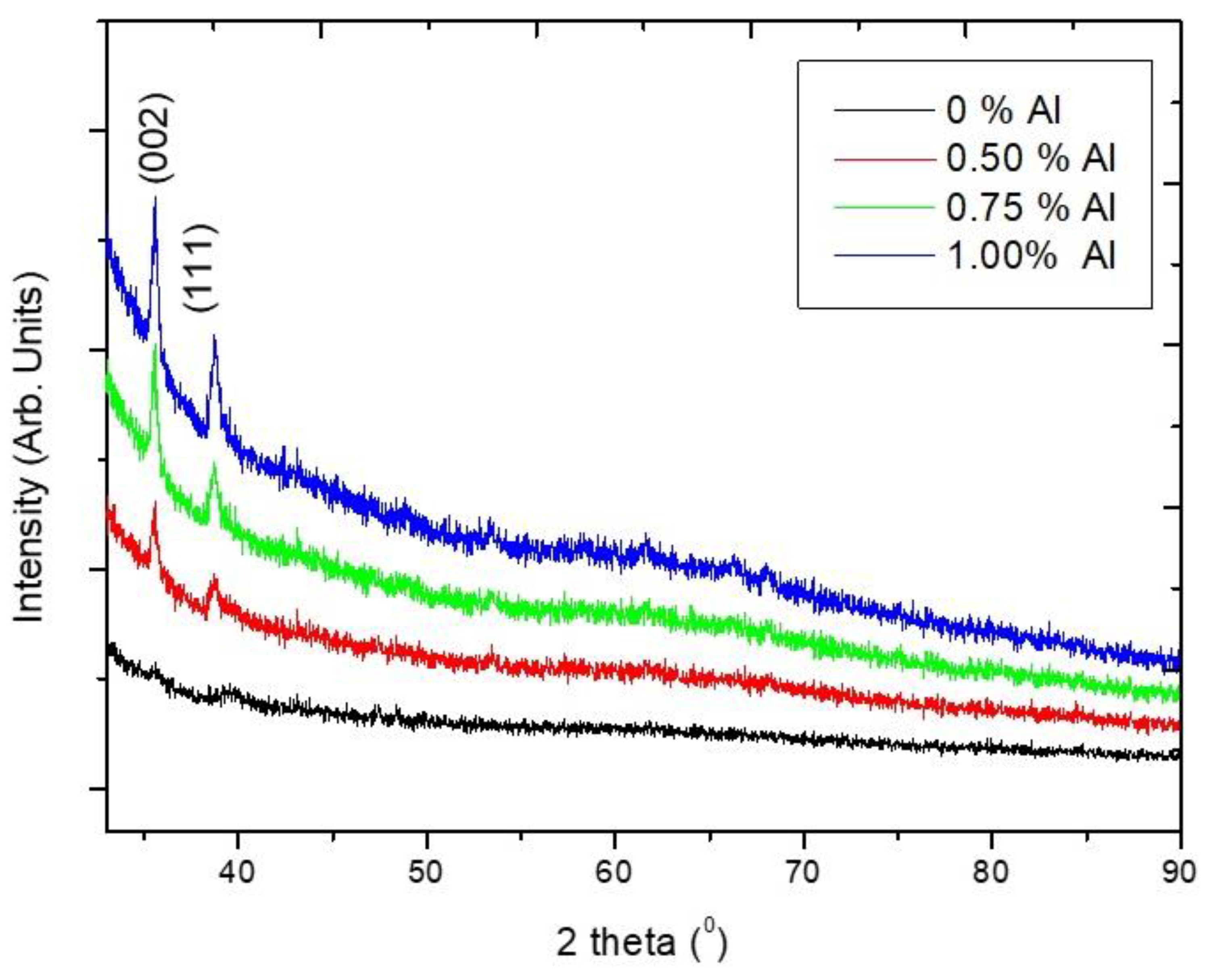
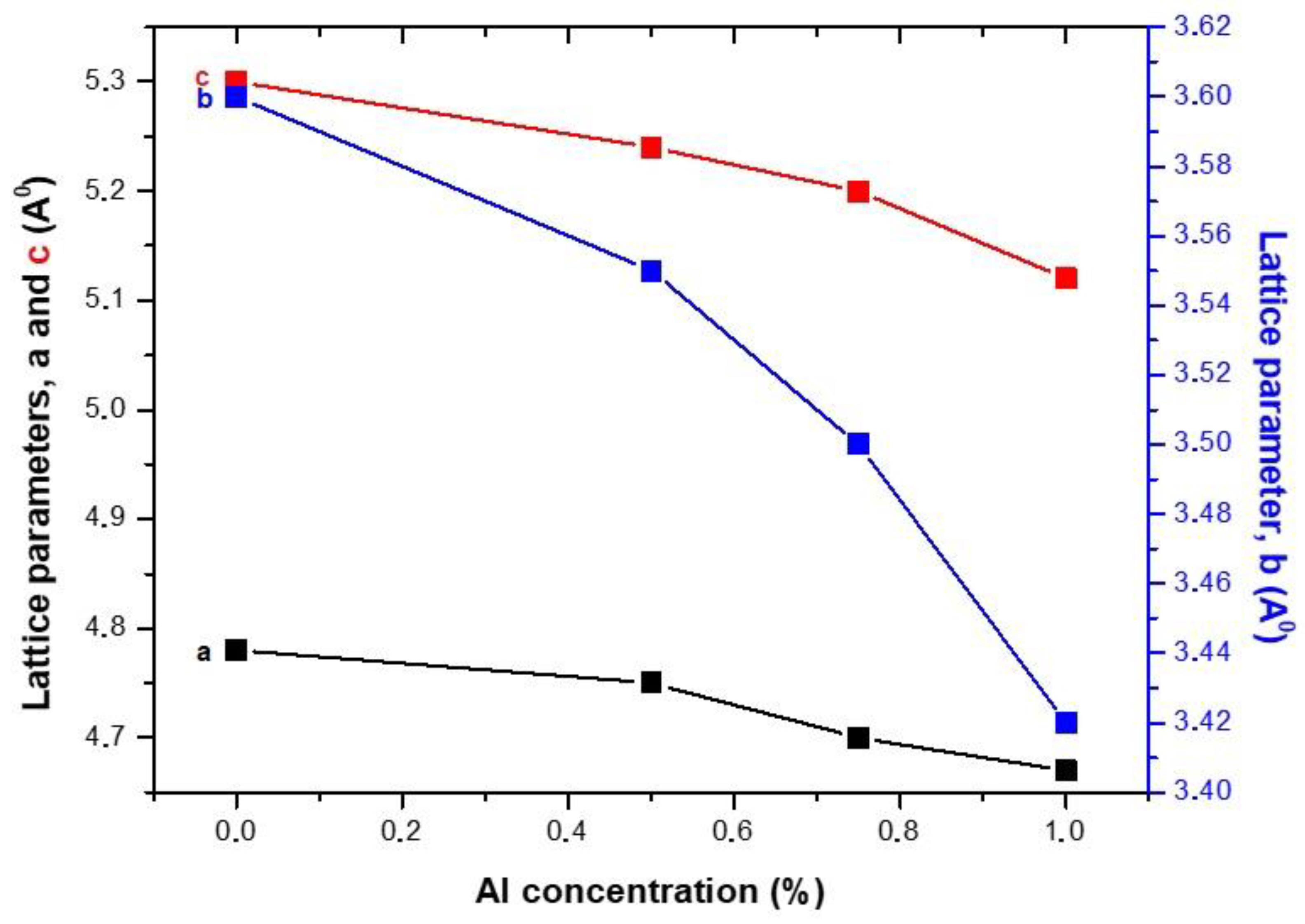
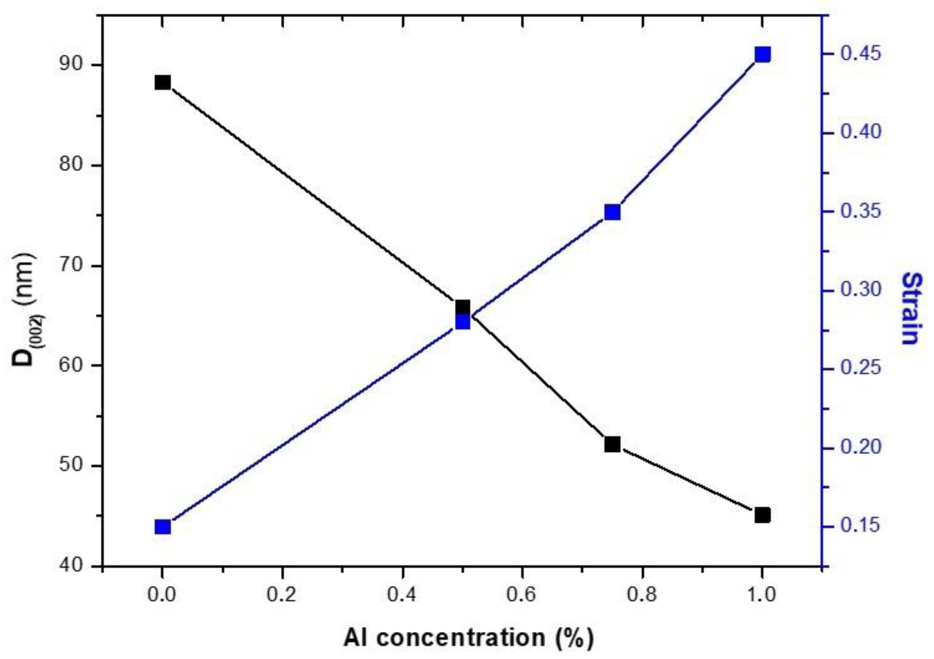
3.1.1. X-ray Diffraction

X-ray diffractograms of Al–doped CuO films grown via spray pyrolysis with varying Al concentrations (0.00, 0.50, 0.75 and 1.00%) are displayed Figure 1.
Two well-defined and sharp peaks are visible, representative of the polycrystalline structure of the deposited films. The most noticeable peaks are observed at 35.59° and 39.11° of the Al:CuO films which correspond to the monoclinic crystal structure of CuO phase alongside the (002) and (111) planes, in accordance with standard data reference (JCPDS card No 045-0937) and in good agreement with literature [16]. The crystal structure of CuO is monoclinic with four CuO units in the unit cell. The primitive cell contains two CuO units with the long direction parallel to the crystallographic c-axis. It is also noteworthy to mention that, as Al doping increases, the intensity of the peaks increases gradually and considerably, indicating that Al favours grain growth and enhances the crystallinity of the parent-phase CuO. Meanwhile, no additional peaks are detected, thereby demonstrating that doping CuO with a small quantity of Al stabilizes the phase stability and its purity. Direct observation of the film via electronic microscopy revealed no other secondary phases. All lattice constants (a, b and c) are determined by using the following equations:
1 d h k l 2 = h 2 a 2 s i n 2 β + k 2 b 2 + l 2 c 2 s i n 2 β 2 h l c o s β a   c   s i n 2 β
λ = 2   d   sin θ
Of course, h, k and l are the Miller indices, while d is the lattice spacing as determined by using Bragg’s Equation (2) and β = 99.45°. All these parameters (a, b and c) of the CuO films are presented in Figure 2, and a gradual decrease with increasing Al concentration is observed.
Lattice parameter as a function of temperature and/or composition is an important piece of information in materials science. The variation in lattice parameter is attributed to the lattice strain induced by the introduction of Al3+ due to the formation of oxygen vacancies. Lattice strain was observed to also decrease with an increase in particle size. However, here it is most remarkable and one should note that the reduction degree of the lattice constant c is relatively more significant compared to that of b and a respectively; i.e., 5.0%, 3.4% and 2.3%. This can be explained by referring to the fact that the Al+3 ionic radius of 0.53 Å is significantly smaller than that of the Cu+2 ions (0.73 Å). Since Al “dissolves” into the CuO host lattice, it tends to occupy the Cu sites, thus inducing the development of the lattice and, as a consequence, a monotonic decrease in the lattice parameters. Micro strain (ε) and crystallite size (D) have been estimated using the main peak (002), by means of the following relationships [19]:
D = 0.9   λ β c o s θ
ε = β   c o s θ 4
where λ is the X-ray beam wavelength, θ is the angle of diffraction, and β is the full width at half maximum of the diffraction peak. From these calculated values, as shown in Figure 3, one observes a significant decrease in crystallite size with increasing Al concentration, i.e., from 88.27 nm for the parent CuO up to 45.1 nm for 1% Al:CuO, representing a reduction of 43%. This demonstrates the polycrystalline nature of the Al:CuO films due to the replacement of Cu+2 ions by Al+3 ions during film formation. This is also explained by the response from the grain boundary. Meanwhile, micro strain increases gradually with increasing Al loading, as shown in Figure 3.

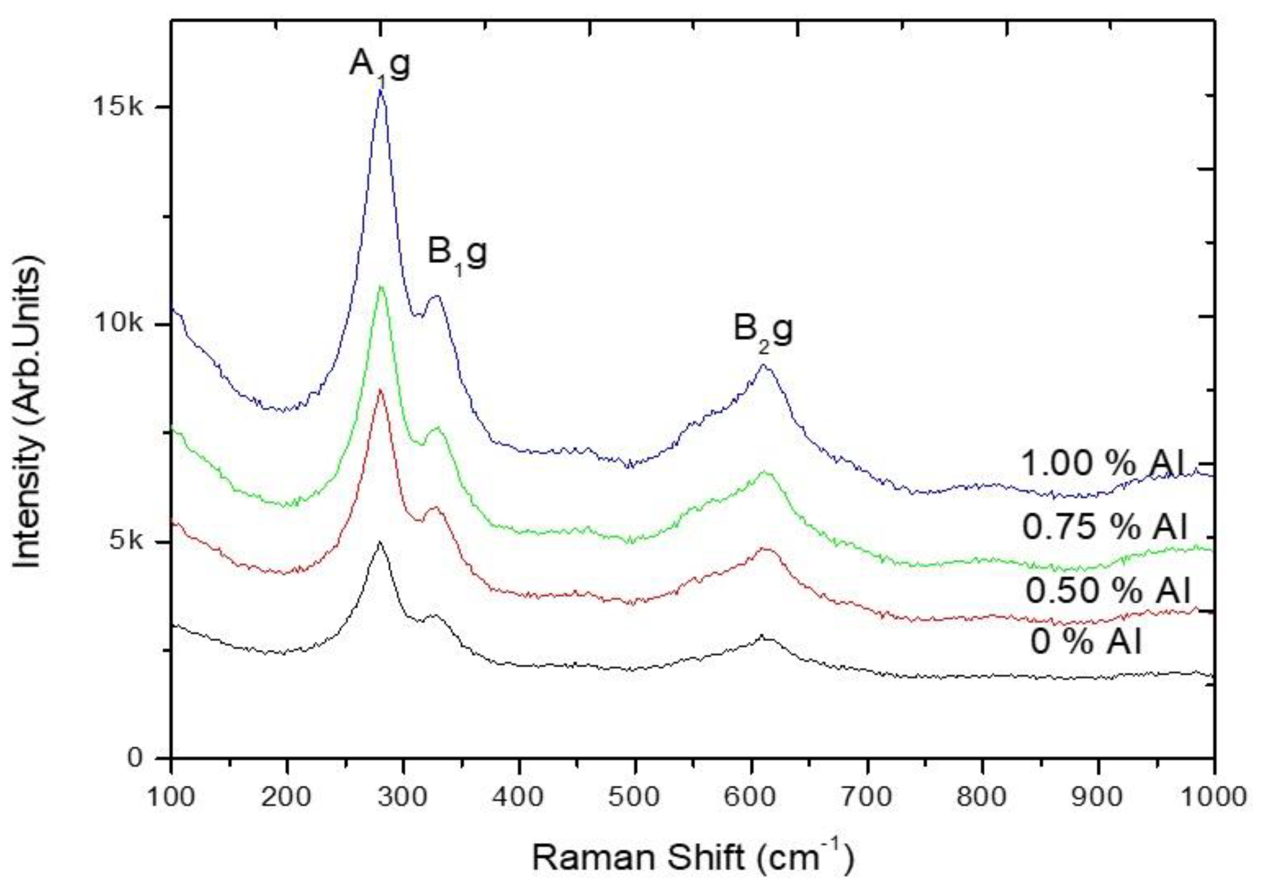
3.1.2. Raman Spectroscopy

Raman spectroscopy is an important scientific technique for probing defects and/or impurities and therefore a powerful tool for revealing the space symmetry of materials. Changes in the characteristic vibrational modes of CuO were studied via Raman scattering experiments, as presented in Figure 4, for pure and Al doped CuO films, at various concentrations of Al. The three Raman active modes predicted by group theory have been identified and their room temperature frequencies determined and subsequently compared to the literature.
The fine shift and broadening of the Raman spectra of CuO crystals are mainly due to doping and size effects. A shift in the Raman spectrum describes phenomena that could be linked to structural disorder and defects (lack of oxygen and/or surface impurities) as well as to potential confinement of phonons. However, a change in polarizability during molecular and/or structural vibration is an essential requirement of obtaining the Raman spectra of samples. Consequently, Raman spectra are made of three main modes, i.e., the Ag and the 2Bg located at 278.94, 330.40 and 616.91 cm−1 respectively. The Raman spectra of CuO samples show that as grain size decreases, the Raman peaks shift to lower wavenumber and become broader owing to size effects. Furthermore, as the segregation of Al dopants takes place in grain boundaries, it is believed to cause an aggravation in crystallinity. Such peaks are widely reported [17,18], thus confirming the presence of a single CuO phase with a monoclinic structure, which reasonably corroborates XRD analysis.

3.2. Electrical Properties

The influence of Al doping on the electrical resistivity of the as-grown Al:CuO thin films is shown in Figure 5. It is clear that resistivity value decreases gradually with Al doping. This can be attributed to two main factors: (i) when the Al+3 ions occupy the Cu+2 ion sites, an additional number of free electrons are created; (ii) the significant reduction in size of the grains generates a huge number of frontiers, and hence an improvement in transport time and/or electron collisions.
The electrical resistivity data obtained in this study are comparable to those obtained by Ziad T. Khodair et al. [20].

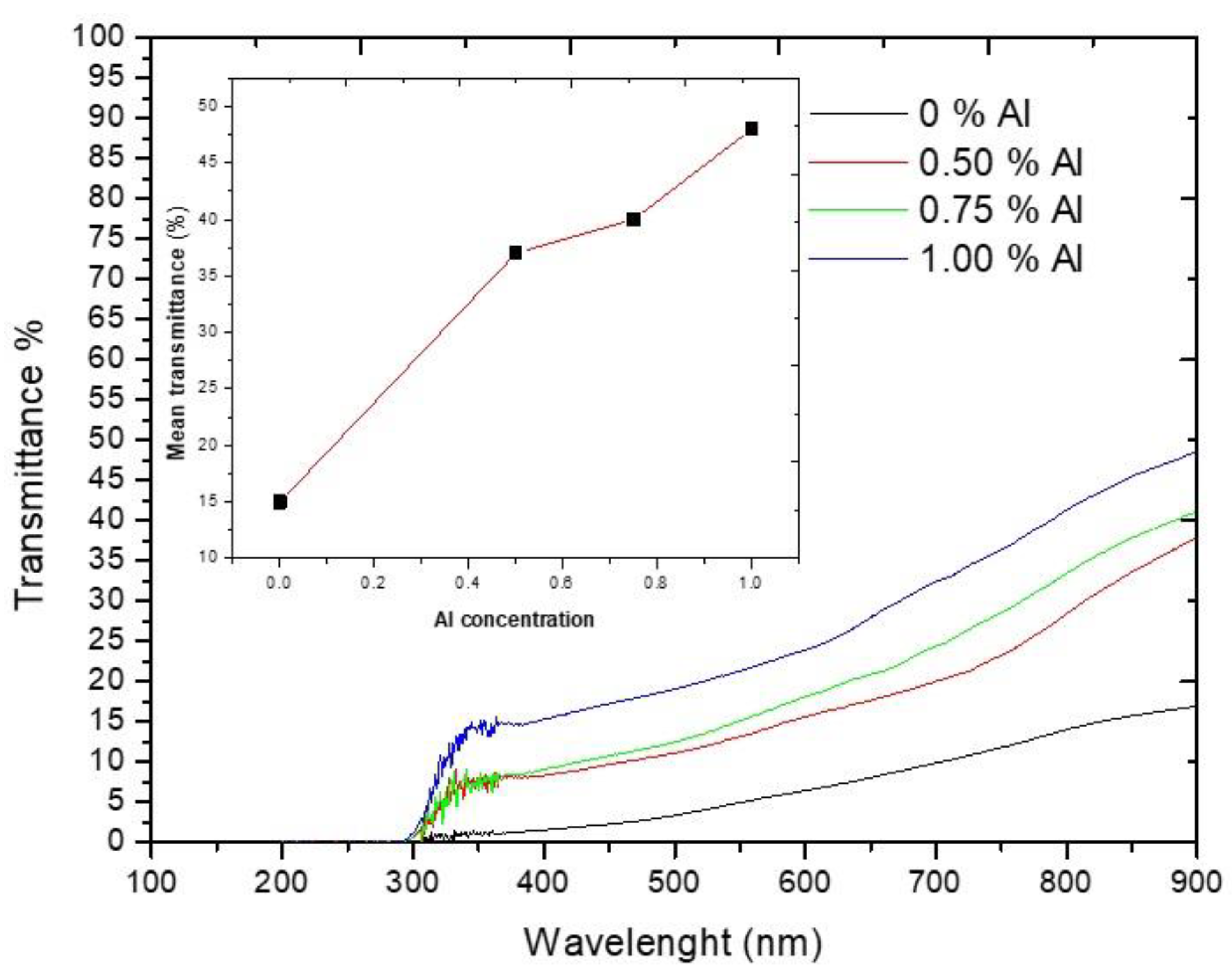
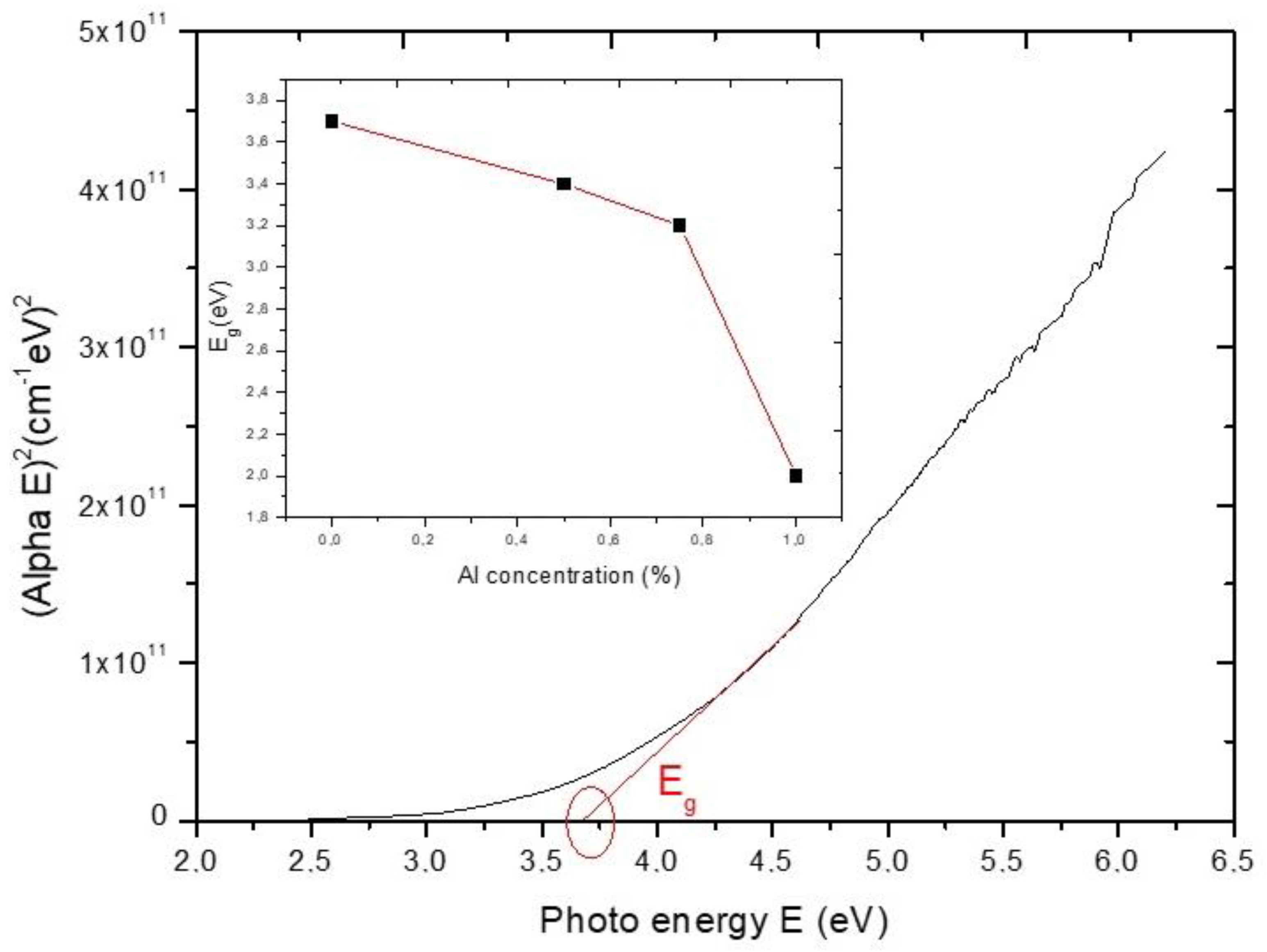
3.3. Optical Properties

The Al:CuO films were optically investigated by recording their transmittance as presented in Figure 6. It can be observed that with the increase in Al doping content, the transmittance was improved significantly from 15% for undoped CuO up to 37% for 0.50% Al, then continued to increase gradually for higher doping (inset of Figure 6), reaching around 48% in the visible wavelength region for 1.00% Al.
The spectra recorded in transmission mode revealed two regions: (i) one that is of high transmission within the infrared region ≥ 900 nm (ii) and a second region with a strong absorption in the visible range. As one may observe, the as-grown Al:CuO films display poor spectral transparency in the visible range.
Next, in order to determine the energy of the optical band gap (Eg), the second region was used by adopting the Tauc relation [23]:
( α h ϑ ) 2 = A ( h ϑ E g )
where A is a constant that characterizes the degree of disorder in an amorphous structure, α is the coefficient of absorption, and is the energy of the photon. The absorption coefficient, calculated by using the Beer Lambert relation [23], is thus:
α = 1 d ln 100 T
where T represents the transmission for a thickness d of CuO film. By plotting (αhϑ)2 vs. , the value of Eg represents the intercept with hv-axis of the straight line. To appreciate the influence of doping and more specifically the doping concentration on sub-band energies and sub-band populations, as well as band bending, several aspects had to be taken into consideration. The variation of the Eg value for Al:CuO films is shown in the inset of Figure 7 as a function of Al doping concentration. One may note that the value of the energy gap gradually decreases with increasing Al doping concentration from 3.7 eV in pure CuO up to 3.4 eV in 0.50 Al:CuO, then suddenly drops drastically up to 2 eV in 1.00 Al:CuO. This can be explained by the following: additional free electrons, reduction of grain size resulting in higher grain boundaries, narrowing of Eg in nanostructured films is associated with quantum confinement. In literature, similar results are reported [24,25,26,27,28].
In brief, the influence of annealing and Al doping upon the optical, electrical and the structural properties of CuO thin films are correlated, presented and discussed. Raman spectroscopy analysis confirms the presence of vibrational bands characteristic of the CuO phase, while X-ray diffraction (XRD) confirms the polycrystalline structure of the pure CuO thin films. Furthermore, XRD analysis of the Al:CuO films indicates that the existence of a monoclinic-type structure (CuO phase) becomes favoured by a preferred alignment alongside the (002) plane with a significant grain size reduction with increasing Al content. Therefore, such a simple synthesis technique, which is both eco-friendly and cost-effective, providing pure or doped CuO thin films, has proven to be suitable in various high-tech applications.
As mentioned earlier herein, CuO has been a top focus among transition metal oxide investigations due to its remarkable properties as a narrow-bandgap p-type semiconductor and as the basis of several high-temperature superconductors and giant magnetoresistant materials. However, increasing requests to develop energy storage systems have inspired academics and engineers to develop innovative materials with superior properties. Hence, the excellent electrochemical properties of CuO have proven to be an even more promising candidate material towards numerous uses such as supercapacitors, lithium batteries and biological sensors for specific molecules (e.g., glucose) [29,30,31,32,33,34,35,36,37,38]. Thus, since CuO is a transition metal compound with a relatively low cost, it could be more than promising as a candidate for an electrode material in supercapacitive applications. Furthermore, electrochemical supercapacitors are well thought out as ultimate high density energy storage devices that will meet pressing requirements in electrical engineering and other applications, such as for the hybrid automotive transportation, due to their long life cycles and high density of power. These preliminary readings suggest that the analysis of electrochemical aspects of CuO is an area of high importance, in particular as thin films and hierarchical structures, and are therefore of paramount importance for such supercapacitor applications. It has also been reported that the materials synthesized by doping aluminium onto CuO improve its light absorption behaviour and have become a good candidate in solar cell applications [39]. Nevertheless, thin film deposition techniques need to be cost-efficient and eco-friendly. Other thin film, multilayer and nanostructure growing techniques, as well as printing, are also being envisaged for our future work, such as pulsed laser deposition (PLD) combined with colloidal lithography and/or other surface structuring techniques [40].

4. Conclusions

Pure and Al–doped CuO thin films were grown on cost-efficient borosilicate (BK7) glass substrates and annealed at 350 °C, using the simple, cost-effective and eco-friendly technique of chemical spray pyrolysis. The monoclinic structure favours an alignment along the (002) and the (111) axes. The results of XRD and Raman spectroscopy revealed that films exhibited a polycrystalline structure. The resulting CuO films exhibited a direct band gap in the range between 1.2 and 2.6 eV. The incorporation of Al resulted in no change to the monoclinic structure of CuO, yet it affected crystallites size. Furthermore, resistivity measurements revealed that resistivity decreased with the increase in Al concentration, while the band gap energy decreased (from 3.7 to 2 eV), while the mean value for the optical transmittance diminished from 48 to 15% between 400 and 800 nm, making it appropriate as an absorber material in photovoltaic applications or as an efficient photocathode in solar water-splitting systems and sensor and optoelectronic industry. Future investigations are due, focused on the interdependence between phase composition, grain size, lattice constant and critical temperature of the resistivity drop with respect to thickness and doping effects in CuO films grown by other techniques, such as pulsed laser deposition, combined with surface structuring techniques.

Author Contributions

Conceptualization, R.D. and C.-D.C.; methodology, R.D., B.B., M.B., M.S.A. and C.-D.C.; investigation, R.D., B.B., M.B. and M.S.A.; writing—original draft preparation, R.D. and C.-D.C.; writing—discussions, review and editing, C.-D.C. and R.D. All authors have read and agreed to the published version of the manuscript.

Funding

This research received no external funding.

Institutional Review Board Statement

Not applicable.

Informed Consent Statement

Not applicable.

Data Availability Statement

The data presented in this study are openly available upon reasonable request from the corresponding and/or first author.

Conflicts of Interest

The authors declare no conflict of interest.

References

  1. Balamurugan, B. Optical and structural properties of nanocrystalline copper oxide thin films prepared by activated reactive evaporation. Thin Solid Film. 2001, 396, 90–96. [Google Scholar] [CrossRef]
  2. Lange, R. Photoelements and Their Applications; Reinhold Publishing Co.: New York, NY, USA, 1939. [Google Scholar]
  3. Seung-Deok, S.; Yun-Ho, J.; Seung-Hun, L.; Hyun-Woo, S.; Dong Wan, K. Low-temperature synthesis of CuO-interlaced nanodiscs for lithium ion battery electrodes. Nano Scale Res. Lett. 2011, 6, 2. [Google Scholar]
  4. Jiang, Y.; Decker, S.; Mohs, C.; Klabunde, K.J. Catalytic solid state reactions on the surface of nanoscale metal oxide particles. J. Catal. 1998, 180, 24. [Google Scholar] [CrossRef]
  5. Chowdhuri, A.; Gupta, V.; Sreenivas, K.; Kumar, R.; Mozumdar, S.; Patanjali, P.K. Response speed of SnO2-based H2S gas sensors with CuO nanoparticles. Appl. Phys. Lett. 2004, 84, 1180–1182. [Google Scholar] [CrossRef]
  6. Hoa, N.D.; An, S.Y.; Dung, N.D.; Quy, N.V.; Kim, D. Synthesis of p-type Semiconducting Cupric Oxide Thin Films and Their Application to hydrogen detection. Sens. Actuators B Chem. 2010, 146, 239–244. [Google Scholar] [CrossRef]
  7. Kari, E.R.; Brown, K.S. Electrochemical synthesis and characterization of transparent nanocrystalline Cu2O films and their conversion to CuO films. Chem. Commun. 2006, 31, 3311–3313. [Google Scholar]
  8. Maruyama, T. Copper oxide thin films prepared from copper dipivaloylmethanate and oxygen by chemical vapor deposition. Jpn. J. Appl. Phys. 2011, 37, 4099–4102. [Google Scholar] [CrossRef]
  9. Oral, A.Y.; Mensur, E.; Aslan, M.H.; Basaran, E. The preparation of copper (II) oxide thin films and the study of their microstructures and optical properties. Mater. Chem. Phys. 2004, 83, 140. [Google Scholar] [CrossRef]
  10. Benjamin, J.H.; Nikolai, K.; Ganhua, L.; Khan, L.I.; Junhong, C.; Xin, Z. Transport analyte detection and optoelectronic response of p-type CuO nanowires. J. Phys. Chem. C 2010, 114, 2440–2447. [Google Scholar]
  11. Zhang, Q.; Zhang, K.; Xu, D.; Yang, G.; Huang, H.; Nie, F.; Liu, C.; Yang, S. CuO nanostructures: Synthesis, characterization, growth mechanisms, fundamental properties, and applications. Prog. Mater. Sci. 2014, 60, 208. [Google Scholar] [CrossRef]
  12. Chen, A.; Long, H.; Yang, G.; Lu, P. Controlled growth and characteristics of single-phase Cu2O and CuO films by pulsed laser deposition. Vacuum 2009, 83, 927. [Google Scholar] [CrossRef]
  13. Chen, F.; Zhang, J.; Wang, G.; Zhang, B.; Miao, X.; Fan, J. CuO nanowires synthesized by thermal oxidation route. J. Alloys Compd. 2008, 454, 268. [Google Scholar] [CrossRef]
  14. Boudjema, B.; Daira, R.; Kabir, A.; Djebien, R. Physico-Chemical Properties of CuO Thin Films Deposited by Spray Pyrolysis. Mater. Sci. Forum 2017, 895, 33–36. [Google Scholar] [CrossRef]
  15. Daira, R.; Kabir, A.; Boudjema, B.; Sedreati, C. Structural and optical transmittance analysis of CuO thin film deposited by the spray pyrolysis method. Solid State Sci. 2020, 104, 106254. [Google Scholar] [CrossRef]
  16. Tan, T.Y. Handbook of Solid State Diffusion; Elsevier Inc.: Amsterdam, The Netherlands, 2017; Volume 1, ISBN 978-0-12-804287-8. [Google Scholar]
  17. Leng, J.; Wang, Z.; Wang, J.; Wu, H.H.; Yan, G.; Li, X.; Guo, H.; Liu, Y.; Zhang, Q.; Guo, Z. Advances in nanostructures fabricated via spray pyrolysis and their applications in energy storage and conversion. Chem. Soc. Rev. 2019, 48, 3015–3072. [Google Scholar] [CrossRef]
  18. Falcony, C.; Aguilar-Frutis, M.A.; García-Hipólito, M. Spray Pyrolysis Technique; High-K Dielectric Films and Luminescent Materials: A Review. Micromachines 2018, 9, 414. [Google Scholar] [CrossRef] [Green Version]
  19. Moumen, A.; Hartiti, B.; Thevenin, P.; Siadat, M. Synthesis and characterization of CuO thin films grown by chemical spray pyrolysis. Opt. Quant. Electron. 2017, 49, 70. [Google Scholar] [CrossRef]
  20. Aroussi, S.; Dahamni, M.A.; Ghamnia, M.; Tonneau, D.; Fauquet, C. Characterization of Some Physical and Photocatalytic Properties of CuO Nanofilms Synthesized by a Gentle Chemical Technique. Condens. Matter 2022, 7, 37. [Google Scholar] [CrossRef]
  21. Tripathi, A.; Dixit, T.; Agrawal, J.; Singh, V. Bandgap engineering in CuO nanostructures: Dual-band, broadband, and UV-C photodetectors. Appl. Phys. Lett. 2020, 116, 111102. [Google Scholar] [CrossRef]
  22. Baturay, S.; Tombak, A.; Batibay, D.; Ocak, Y.S. n-Type conductivity of CuO thin films by metal doping. Appl. Surf. Sci. 2019, 477, 91. [Google Scholar] [CrossRef]
  23. Mashhad-toroghi, A.H.; Shahtahmasebia, N.; Azhira, E.; Madahia, P.; Mashreghi, M. Deposition of Copper Oxide Nanostructured Thin films and Study of the Influence of Fe3+ Doped on the Structural, Optical and Antibacterial Properties of CuO Thin Films. In Proceedings of the 4th International Conference on Nanostructures ICNS4, Kish Island, Iran, 12–14 March 2012; pp. 852–854. [Google Scholar]
  24. Volanti, D.P.; Keyson, D.; Cavalcante, L.S.; Simões, A.Z.; Joya, M.R.; Longo, E.; Varela, J.A.; Pizani, P.S.; Souza, A.G. Synthesis and characterization of CuO flower-nanostructure processing by a domestic hydrothermal microwave. J. Alloys Compd. 2008, 459, 537–542. [Google Scholar] [CrossRef]
  25. Yu, T.; Sow, C.H.; Gantimahapatruni, A.; Cheong, F.C.; Zhu, Y.; Chin, K.C.; Xu, X.; Lim, C.T.; Shen, Z.; Thong, J.T.L.; et al. Patterning and fusion of CuO nanorods with a focused laser beam. Nanotechnology 2005, 16, 1238. [Google Scholar] [CrossRef]
  26. Dennis, B. Elements of X-ray Diffraction, 3rd ed.; Prentice-Hall International: Upper Saddle River, NJ, USA, 2000. [Google Scholar]
  27. Khodair, T.Z.; Shallal, N. Effect of Aluminum Doping on Structural Properties of CuO Thin Films Prepared by Chemical Spray Pyrolysis (CSP) Technique. Diyala J. Pure Sci. 2017, 13, v198–v208. [Google Scholar] [CrossRef]
  28. Pankove, J.I. Optical Processing in Semiconductors; Dover: New York, NY, USA, 1971. [Google Scholar]
  29. Moumen, A.; Hartiti, B.; Comini, E.; El Khalidi, Z.; Arachchige, H.M.M.; Fadili, S.; Thevenin, P. Preparation and characterization of nanostructured CuO thin films using spray pyrolysis technique. Superlattice Microst. 2019, 127, 2–10. [Google Scholar] [CrossRef]
  30. Ravichandran, A.T.; Dhanabalan, K.; Valanarasu, S.; Vasuhi, A.; Kathalingam, A.J. Role of immersion time on the properties of SILAR deposited CuO thin films. Mater. Sci. Mater. Electron. 2015, 26, 921. [Google Scholar] [CrossRef]
  31. Jundale, D.M.; Joshi, P.B.; Sen, S.; Patil, V.B. Nanocrystalline CuO thin films: Synthesis, microstructural and optoelectronic properties. J. Mater. Sci. Mater. Electron. 2012, 23, 1492. [Google Scholar] [CrossRef]
  32. Daira, R.; Boudjema, B. Application of laser technique for the calculating the speckle size and object incidence angle. J. Intense Pulsed Lasers Appl. Adv. Phys. 2015, 5, 1–4. [Google Scholar]
  33. Daira, R.; Boudjema, B.; Mordjaoui, M.; Mezéri, M. Electrical properties of metallophthalocyanine thin films. J. Optoelectron. Adv. Mater. Rapid Commun. 2011, 5, 167–171. [Google Scholar]
  34. Konar, S.; Kalita, H.; Puvvada, N.; Tantubay, S.; Mahto, M.K.; Biswas, S.; Pathak, A. Shape-dependent catalytic activity of CuO nanostructures. J. Catal. 2016, 336, 11. [Google Scholar] [CrossRef]
  35. Dubal, D.P.; Gund, G.S.; Lokhande, C.D.; Holze, R. CuO cauliflowers for supercapacitor application: Novel potentiodynamic deposition. Mater. Res. Bull. 2013, 48, 923–928. [Google Scholar] [CrossRef]
  36. Li, J.; Su, Q.; Du, G. Facile synthesis of flowerlike CuO by double-hydroxides treatment and their electrochemical properties. Mater. Lett. 2012, 84, 97. [Google Scholar] [CrossRef]
  37. Patake, V.D.; Joshi, S.S.; Lokhande, C.D.; Joo, O.-S. Electrodeposited porous and amorphous copper oxide film for application in supercapacitor. Mater. Chem. Phys. 2009, 114, 6. [Google Scholar] [CrossRef]
  38. Wang, X.; Hu, C.; Liu, H.; Du, G.; He, X.; Xi, Y. Synthesis of CuO nanostructures and their application for nonenzymatic glucose sensing. Sens. Actuators B Chem. 2010, 144, 220. [Google Scholar] [CrossRef]
  39. Arfan, M.; Siddiqui, D.N.; Shahid, T.; Iqbal, Z.; Majeed, Y.; Akram, I.; Bagheri, R.; Song, Z.; Zeb, A. Tailoring of nanostructures: Al doped CuO synthesized by composite-hydroxide-mediated approach. Results Phys. 2019, 13, 102187. [Google Scholar] [CrossRef]
  40. Al-Kattan, A.; Grojo, D.; Drouet, C.; Mouskeftaras, A.; Delaporte, P.; Casanova, A.; Robin, J.D.; Magdinier, F.; Alloncle, P.; Constantinescu, C.; et al. Short-Pulse Lasers: A Versatile Tool in Creating Novel Nano-/Micro-Structures and Compositional Analysis for Healthcare and Wellbeing Challenges. Nanomaterials 2021, 11, 712. [Google Scholar] [CrossRef] [PubMed]
Figure 1. XRD of pure and Al–doped CuO films grown at 350 °C via spray pyrolysis.
Applsci 13 08193 g001
Figure 2. Variation of the lattice parameters (a and c) of pure and Al–doped CuO films grown at 350 °C via spray pyrolysis as a function of Al concentration.
Applsci 13 08193 g002
Figure 3. Variation of the (002)-oriented crystallite size and the micro strain of pure and Al–doped CuO films grown at 350 °C via spray pyrolysis as a function of the Al concentration.
Applsci 13 08193 g003
Figure 4. Raman spectra of pure and Al–doped CuO thin films grown at 350 °C via spray pyrolysis on glass substrates.
Applsci 13 08193 g004
Figure 5. Variation of the resistivity of pure and Al–doped CuO films grown at 350 °C via spray pyrolysis as a function of the Al concentration.
Applsci 13 08193 g005
Figure 6. UV–visible transmittance spectra of pure and Al–doped CuO thin films grown at 350 °C via spray pyrolysis as a function of the Al concentration.
Applsci 13 08193 g006
Figure 7. Typical (αhϑ)2 vs. hv plot of pure and Al–doped CuO films grown at 350 °C via spray pyrolysis as a function of Al concentration. Inset presents the variation of the energy band gap Eg as a function of Al concentration.
Applsci 13 08193 g007
Disclaimer/Publisher’s Note: The statements, opinions and data contained in all publications are solely those of the individual author(s) and contributor(s) and not of MDPI and/or the editor(s). MDPI and/or the editor(s) disclaim responsibility for any injury to people or property resulting from any ideas, methods, instructions or products referred to in the content.

