1. Introduction
Vertical power MOSFETs based on silicon [
1] and silicon carbide [
2] devices, intended for the automotive sector, need a considerable cutdown of the switching losses and Joule heating effect [
3,
4]. A method to achieve this consists of reducing the thickness of the semiconductor wafer. However, the combined effect of a thinned substrate along with, e.g., a front side metallization (FSM) produces a severe warpage of the whole wafer, which can hinder the performance and subsequent manufacturing processes needed to complete the devices.
Containing the warpage of the wafer determined by the FSM residual stress is crucial in the semiconductor industry. Indeed, the handling of the wafer as the size increases can be an issue; also in the case of SiC substrates [
5,
6]. A method to solve the issue involves the use of taiko wafers [
7,
8,
9,
10,
11,
12], which consists of back-ground wafers having a ring region of the wafer which is preserved. The result is that, because of the intrinsic structure of the taiko wafer, for a given metal stress and metal film thickness, the resulting warpage of a FSM-thinned wafer is mitigated with respect to the case of a canonical or flat metallized thinned wafer.
To gain an analytical description of the system, we start with the simplification of a disk-shaped wafer. A thin FSM metal film, deposited on the front side of a semiconductor wafer, warps the whole metalized wafer until the net forces and the resulting bending moment’s zero-condition is reached. From this it is possible to gain an estimate of the resulting curvature. If the substrate thickness
is constant and negligible with respect to the diameter
, of the wafer, by considering a thickness
of the film, uniform and small compared to that of the substrate, an average film stress,
, can be determined from the curvature of the elastically deformed coated substrate, according to the equation proposed by Stoney [
13], which, corrected with the biaxial modulus [
14] can be written as:
Equation (1) provides a direct linear relationship between the measured average curvature and the average film stress . In the equation and are the Young’s modulus and Poisson ratio of the substrate, respectively.
In general, the Stoney equation is appropriate in the linear regime where both the residual stress
and the resulting curvature
are low. However, as the stress increases, deviations from linearity are observed and the curvature
for a given stress
of the film becomes lower than what is predicted by Equation (1). Corrections to the Stoney equation have been considered in the past. For example, a cubic polynomial correction to the linear dependence, has been proposed [
15].
Additionally, an effort to extend Stoney’s formula for non-uniform wafer thickness has been made in [
16] for the case of wafers with a slight thickness change in the peripheral region. However, this work only considers the step as a small disturbance compared to the overall wafer thickness, thus it does not offer a comprehensive solution in the case of a taiko wafer.
Approaches based on Finite Element Analysis (FEA) have also been considered in the case of flat substrates using standard structural analysis tools such as ANSYS [
17,
18,
19] and ABAQUS [
20]. These works highlight that it is challenging to accurately predict the final shape of the warped flat substrate. Indeed, a numerical and stable solution is often not the physical one, unless a small perturbation which would result in a bifurcation, is applied. As far as we are aware, there have been few comprehensive studies on general cases of taiko wafers. The way the warpage changes for these wafers is therefore unclear. In this study, we offer an analytical explanation derived from the theory of elasticity to comprehend the resulting warpage in an FSM-taiko wafer. Indeed, in 2021, Vinciguerra and Landi [
21] introduced an analytical method to model the bifurcation in back-side metalized taiko wafers. In the following years, with Malgioglio, they reported on their investigation of the bifurcation phenomenon in 8” metalized wafers [
22,
23,
24,
25,
26] by means of FEA methods and extended the investigation to understand the correlation between warpage wafer and warpage die [
27]. The aim of this work is to compare the analytical description of the warpage occurring in an FSM-taiko wafer with the results obtained by Finite Element Simulations of the same system achieved by means of the ANSYS
® mechanical solver.
In fact, the Stoney equation is not valid for the case of a taiko wafer since we have to consider the presence of the ring. In the current study we aim to expand the analysis of warpage to the case of a taiko wafer that has been metalized on the front side. Specifically, we aim to investigate the warpage of a front side metal (FSM) taiko wafer in the spherical regime and determine the value of the equivalent thickness for an FSM-taiko wafer.
The equivalent thickness concept in the context of a taiko wafer involves making modifications to the mathematical Equation (1), to account for the effects of the wafer’s physical properties and determine the influence of the ring region on its warpage. This includes considering the wafer as an idealized structure with a constant curvature, despite the presence of a damaged layer due to back-grinding [
28].
A proposal for a modified Stoney formula for a taiko wafer can be written as:
where
is the bending moment determined by the FSM and
is the flexural rigidity of the FSM-taiko wafer. A rigorous determination of the values for these quantities involves the use of the theory of elasticity [
29,
30].
In this work we considered a novel approach, which consisted of developing an analytical model of the curvature determined by the stress produced by an FSM in a taiko wafer and compared the result with a finite element analysis (FEA) method of the same metalized taiko wafer, which was achieved by using the ANSYS mechanical solver. The novelty of the method lies in the fact that developing the equations which rule the curvature of the taiko wafer will allow an understanding of the physics which determine the mitigation of the warpage in these kinds of wafers. To do so, we define first all the quantities which are involved in the description of an FSM taiko wafer.
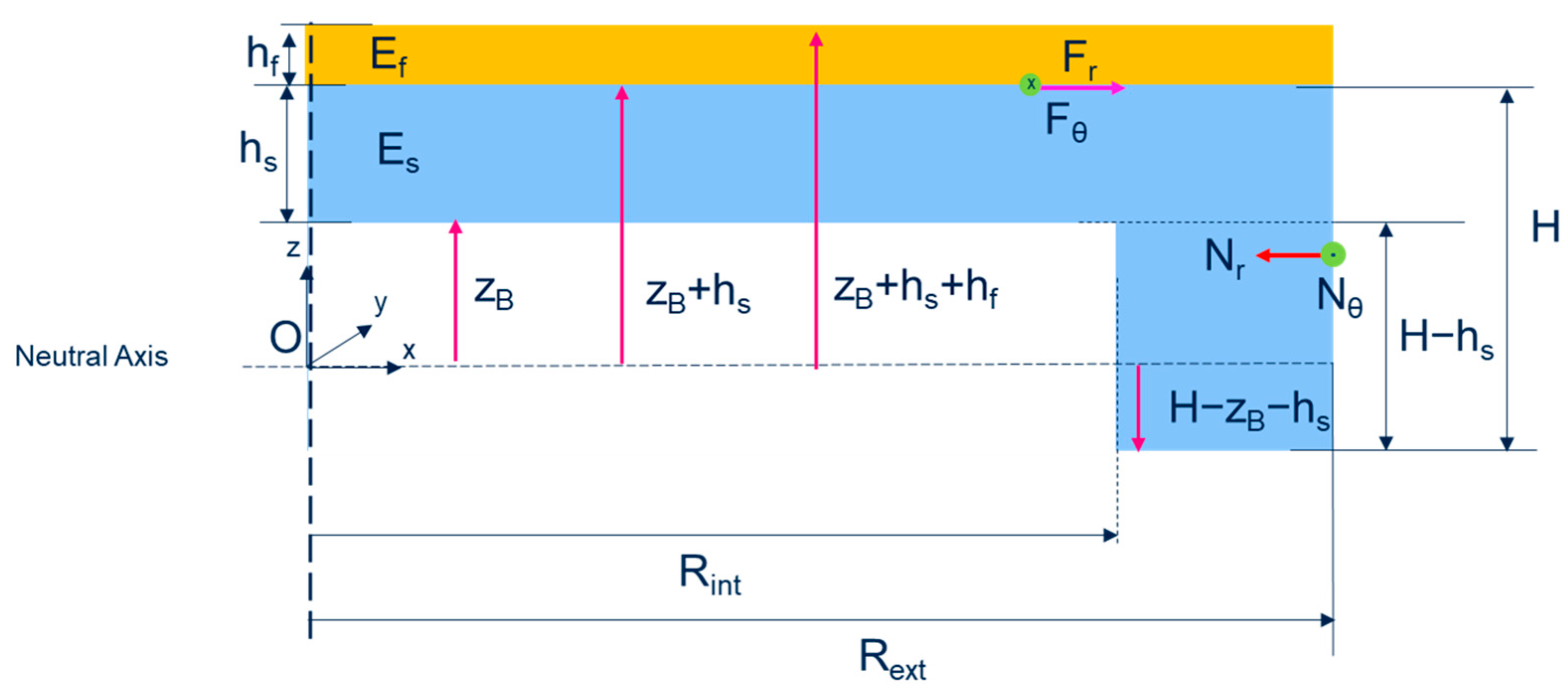
In
Figure 1 the schematic of half of the vertical cross-section of an FSM-taiko wafer is reported. A reference frame is fixed at the center of the taiko wafer, with the origin placed on the neutral plane, such that the back side of the wafer is at
with respect to the neutral plane. In the schematic,
is the thickness of the substrate,
the height of the ring region,
the internal radius and
the external radius, respectively. On the front side of the wafers a thin film, e.g., metal, having a modulus of elasticity
and thickness
, is indicated in yellow. The neutral axis results from the intersection of the neutral plane and the cross-section plane. Once the reference is fixed,
is the distance between the neutral axis (plane) and the interface substrate/thin film,
is the distance between the neutral axis and the FSM thin film top-surface, whereas
is the distance of the ring region surface of the taiko wafer with respect to the neutral axis. The height of the step is given by
and usually is a fixed quantity.
In
Table 1 we report the typical value of the geometrical quantities involved in the investigation of the FSM taiko wafer.
2. Warpage of an FSM Taiko Wafer According to the Theory of Elasticity in the Spherical Case
In analogy to what reported in [
21], we can develop an approximation of the warpage of a front side metalized taiko wafer. Indeed, according to the theory of elasticity (see Landau–Lifshitz [
29]), if the taiko wafer is not subject to the force of gravity, the vertical displacement
with respect to the neutral surface satisfies the biharmonic equation
, which is valid in the ring region as well as in the thinned wafer region.
For a FSM taiko wafer as well, the biharmonic equation has the Michell’s solution [
31]. However, in the spherical case, as a first approximation, the warpage can be characterized by one curvature
in the substrate region and one curvature
in the ring region. In detail, in the ring region,
, the simplest solution does not consider the dependence on the angle
and can be written as:
In the internal and thinned substrate region,
, the spherical solution of the biharmonic equation is
The curvatures , and the parameters , b, c and d can be determined from the boundary conditions and .
At the interface between the FSM thin film and the wafer substrate, at a distance
from the center, the taiko wafer is subject to a radial and a circumferential force, whose values per unit length are set equal to
and
, respectively (See
Figure 1).
The wafer is considered supported at the external ring
, and
and
are the reaction forces evaluated per unit length (See
Figure 1).
Because of the mechanical equilibrium, the resultant forces and moments must be equal to zero. In particular, the equilibrium of forces and moments holds locally for the thin film deposited in the substrate region:
Additionally, the reaction moments acting on the ring at
are in equilibrium with those of the substrate.
By similar reasoning to the case of [
21], the moments per unit length in the substrate region and ring region can be written as:
where
and
are the flexural rigidity of the substrate and ring regions, respectively. Whereas
and
are the moments of inertia of a section of the taiko wafer, considered as a beam of width
, with respect to the neutral axis [
32], in the substrate and ring region, respectively.
Being , the forces per unit length acting on the length , the moment equals .
Since
, and
, in the limit
,
, which implies that
. Moreover, in the limit
,
, and according to the Stoney formula
, which implies that
. Hence, the set of four equations for the moments can be written as:
In general, and are functions of , such that in the limit , .
The equation
is the extension of the Stoney formula for the case of an FSM taiko wafer. It can be solved once that
and
are known.
4. Evaluation of
To gain the mechanical stress , of the thin metal film, from measurement of warpage we need to evaluate . This quantity can be calculated from the equilibrium of the forces.
In the substrate region by following [
33], we can write the total force acting in the substrate region in the radial direction as:
where
and
.
At a given distance
we can write,
and the total force acting on the substrate region is
being
.
In the ring region we need to evaluate the quantity:
Hence, in the case of the taiko wafer, the total force acting on the taiko wafer, in the radial direction, equals zero, being in equilibrium:
In the limit
,
, Equation (19) reduces to the canonical case of a flat disk wafer:
where
is equal to
which is the value of the limit
if
. Moreover, if
,
.
To evaluate
in the general case, it is necessary to combine, the modified Stoney formula for the taiko wafer (Equation (9)) and calculate the value of the integral (see Appendix B of [
21] according to the function
evaluated in Appendix A in [
21]. By doing so, a linear equation is obtained, whose solution provides the value of the neutral axis
where
is the normalized function reported in Equation (A1) of Appendix A of ref. [
21].
By developing the calculations, we have that the neutral plane
is given by:
If
, this expression is simplified as
The normalized integral
has been evaluated and its value is also reported in Appendix B of [
21].
By substituting the value of
in Equation (9) we find that the curvature can be expressed as:
By considering the Stoney approximation in Equation (1), we can express a new quantity, defined as the equivalent thickness of a FSM taiko wafer, which is the thickness that a plain wafer should have to determine the same slope in the curvature–stress curve
. The equivalent thickness of a taiko wafer can hence be determined from Equation (27):
and expressed as
In the specific case of Equation (26), the equivalent thickness of a taiko wafer depends on
as
As in the case reported in [
21], besides the equilibrium of the forces in the radial direction, the net forces along the circumferential
direction must also be considered. In the case of an FSM-taiko wafer, the net forces in the
direction must satisfy equation:
which leads to an additional value of
that can be simplified, if
, as
Additionally, in this case the normalized integral
has been evaluated and reported in Appendix B of [
21].
At the end it is possible to calculate an additional value of
, which determines the curvature
And hence an additional value of the slope .
To summarize, there are two values of
, a value determined by Equation (26), hereafter indicated as
, which determines a neutral axis along the radial direction, because of the radial net force, and a value determined by Equation (34), hereafter indicated with
, which determines an additional neutral axis in the radial direction determined by the equilibrium of the net circumferential forces.
Table 2 reports the numerical quantities of the integrals
I1 and
I2 for the typical values of the parameters of a FSM taiko wafer.
5. ANSYS Finite Element Model of an FSM-Taiko Wafer in the Spherical Case
Along with the analytical approach reported in the previous section, an investigation of the FSM-taiko wafer has been carried out by realizing the finite element method (FEM) simulations with the software tool ANSYS
® Mechanical Enterprise 2022/R2. The geometry of the system is the same as the one reported in
Figure 1. The mechanical behavior of a system consisting of a 200 mm (8″) taiko silicon wafer, coated with a 4.5 μm Al metal layer on the front side, has been simulated in the spherical case.
The simulations conditions were the following. Mesh preferences were set as non-linear mechanical. A regular radial mesh was optimized by dividing the geometry model of the silicon wafer and Al layer into 12 parts resulting from the intersections of three concentric rings with four quadrants, for a total of 28 parts, by considering both the silicon substrate and the aluminum layer. Moreover, the taiko wafer was laid on four supports, symmetrically positioned at the edge. Each support consists of an elastic facet having dimensions of 4 mm × 3 mm, whose foundation stiffness was set equal to 1 N/mm
3. The face-to-face contacts between the silicon and aluminum layers were set as bonded with a tolerance of
mm. In the FEM analysis the physics chosen was the Static Structural with physics type structural and solver target Mechanical APDL. A direct solver type was used by setting the large deflection to on, and the weak springs condition has been set to on. In
Figure 2a,b a snapshot of the top plan-view and rear plan-view of the simulated taiko wafer film, with the ring region and the four supports highlighted, is shown. In
Figure 2c a magnification of the pin region is reported.
The silicon substrate (001) has been simulated by taking into account of its elastic constants opportunely chosen according to the face orientation to reproduce a Young’s modulus of ESi = 130 GPa and Poisson’s ratio and νSi = 0.27, respectively. The Al layer has been considered as an isotropic material, with a Young’s modulus of EAl = 68 GPa and νAl = 0.33, respectively. The coefficients of thermal expansion (CTEs) of silicon and aluminum have been gained from a set of values tabulated at specific temperatures and then interpolated for intermediate values. For each simulation a thermal load was applied to the whole system, by considering the stress-free condition at the higher nominal temperature T of the environment. The FSM-taiko wafer was cooled down from the nominal temperature T in °C to the temperature of 25 °C. Temperatures parametrized from 30 °C up to 170 °C have been simulated.
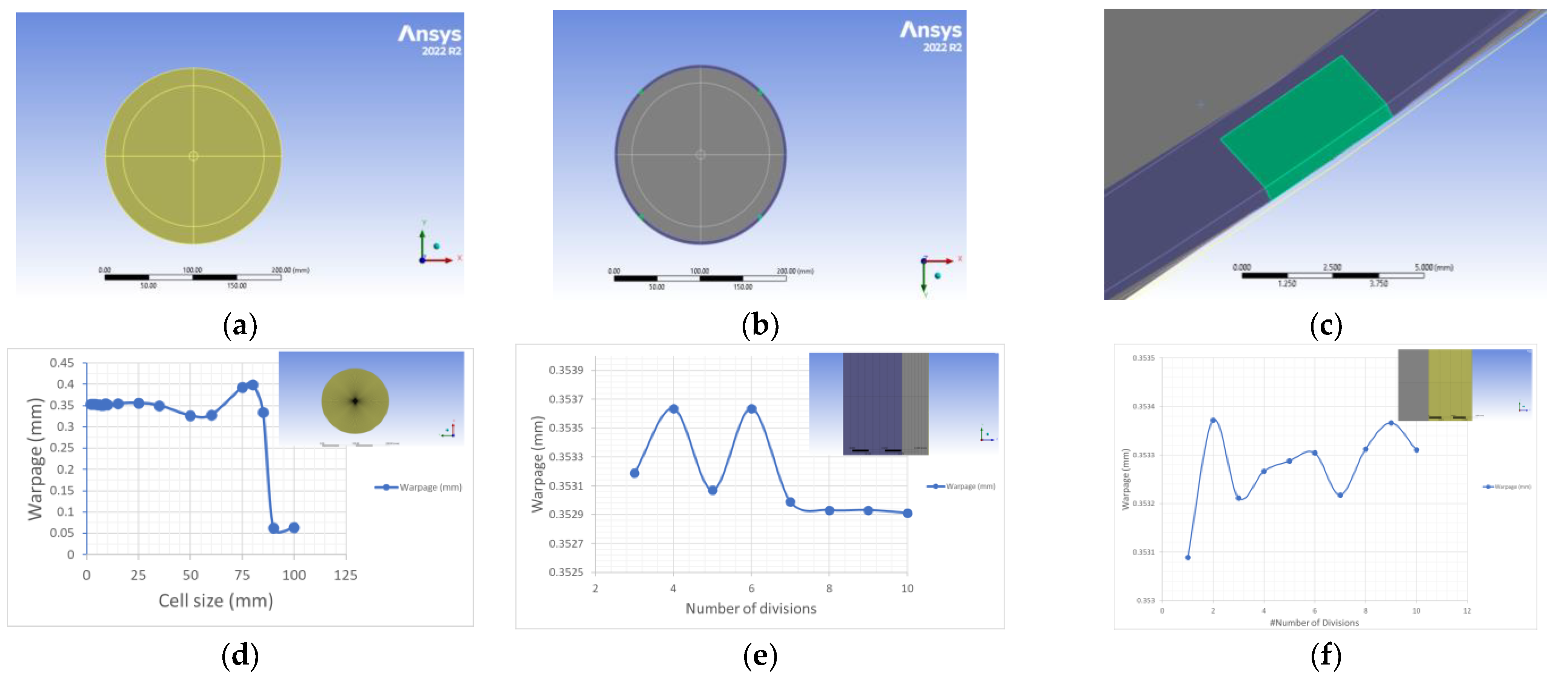
A mesh converge study has been carried out and reported in
Figure 2d–f. All the 28 regions were divided into a set of cells characterized by a planar size in the order of millimeters and by two edge divisions determining a “slicing” of the metal layer and the set formed by the ring region and the substrate region. For the mesh convergence investigation, we monitored the warpage, that is the directional deformation in the z direction, of an FSM taiko wafer having a substrate central thickness of 200 µm when the wafer was cooled down from the temperature of 50 °C to 25 °C. It results that the size of the cell in the xy plane rules the FEM convergence of the whole system. Indeed, as reported in
Figure 2d, as the size of the cell reaches the order of 10 mm the value of the resulting deformation stabilizes. Whereas, the convergence is stable with respect to the number of divisions in the substrate region and ring region as reported in
Figure 2e, as well as with respect to the number of divisions in the metal layer (see
Figure 2f). To reach a compromise between accuracy and time required for the simulations we have determined that a size of 3 mm for the planar mesh, a number of divisions equal to two for the metal layer and a number of divisions equal to three for the substrate and also equal to three for the ring region, suffice to achieve an accurate convergence.
6. ANSYS Results
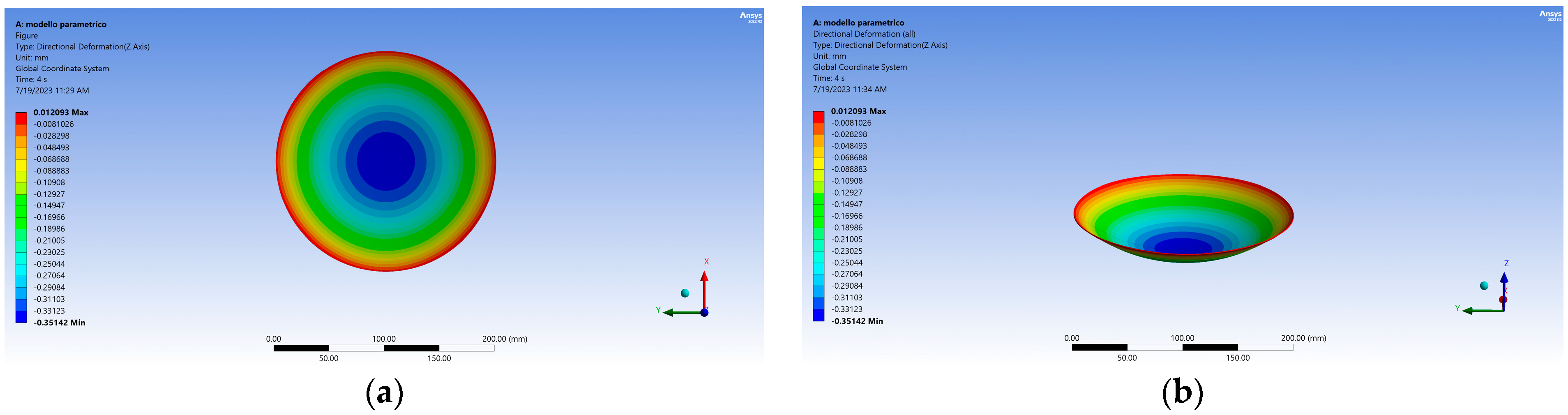
For a given nominal temperature T, we measured the equivalent von Mises stress of the FSM layer and the warpage of the taiko wafer. In particular, the warpage was probed by determining the directional deformation along the z direction of the whole system, as well as on a set of three pairs of paths extending along the diameter of the wafer. Each pair of these pathswas oriented according to two perpendicular directions, the x and y direction of the coordinate system. Of the three pairs, the first pair of paths was set at the top of the Al layer, the second pair of paths at the interface between the Si substrate and the Al layer and the third pairs at the bottom of the central region of the taiko wafer. The value of the warpage was recorded for each nominal temperature and the curvature calculated. In
Figure 3a we report the distribution of the directional deformation along the z direction for a taiko wafer 200 µm thin, simulated at a nominal temperature of T = 50 °C. All the other quantities have been set to the typical values. In
Figure 3b we report the projection of the distribution of the directional deformation in the z direction for the same 200 µm thin taiko wafer, simulated at a nominal temperature of T = 50 °C. The magnification is 100×. In
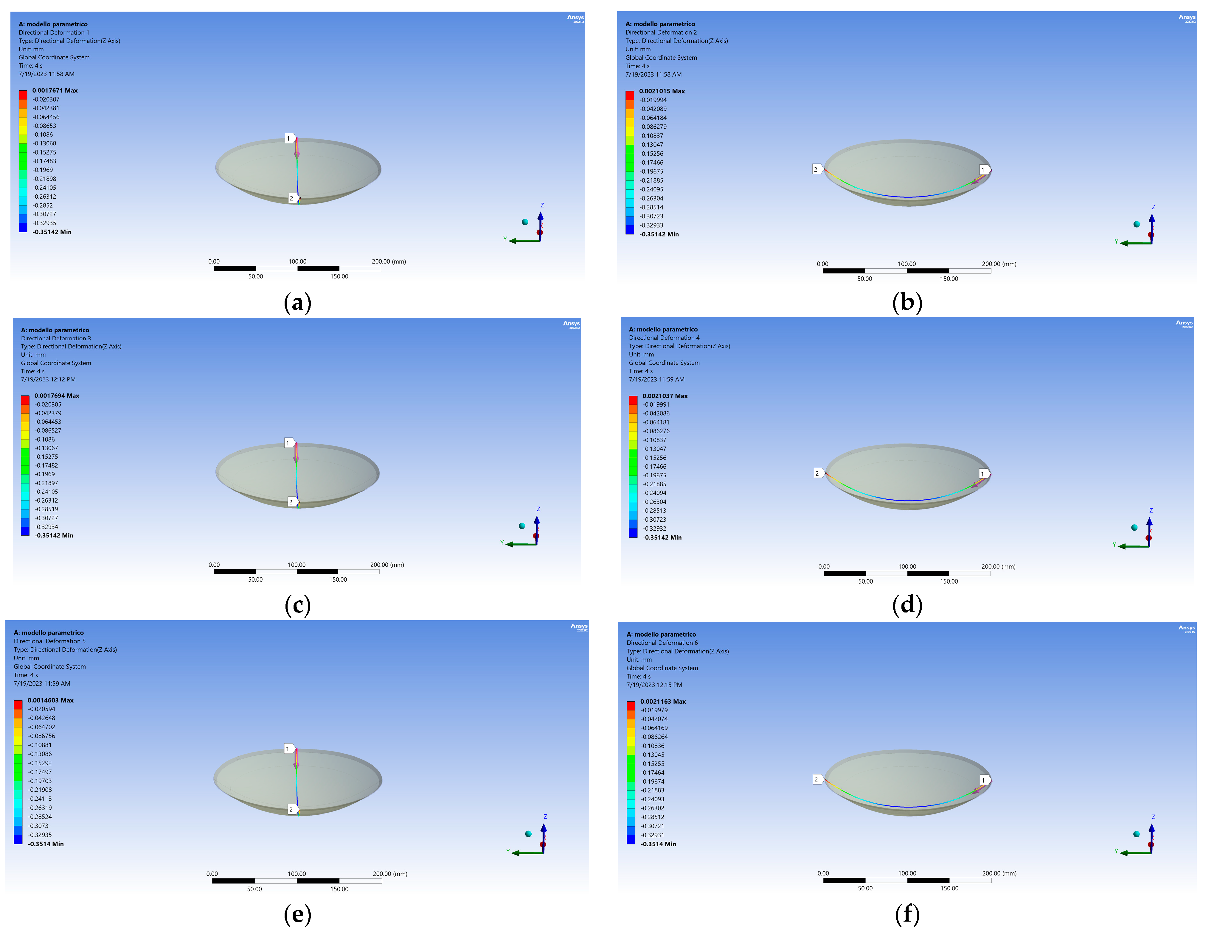
Figure 4 from a to f we report the indication of the three pairs of x- and y-paths for this specific case.
In
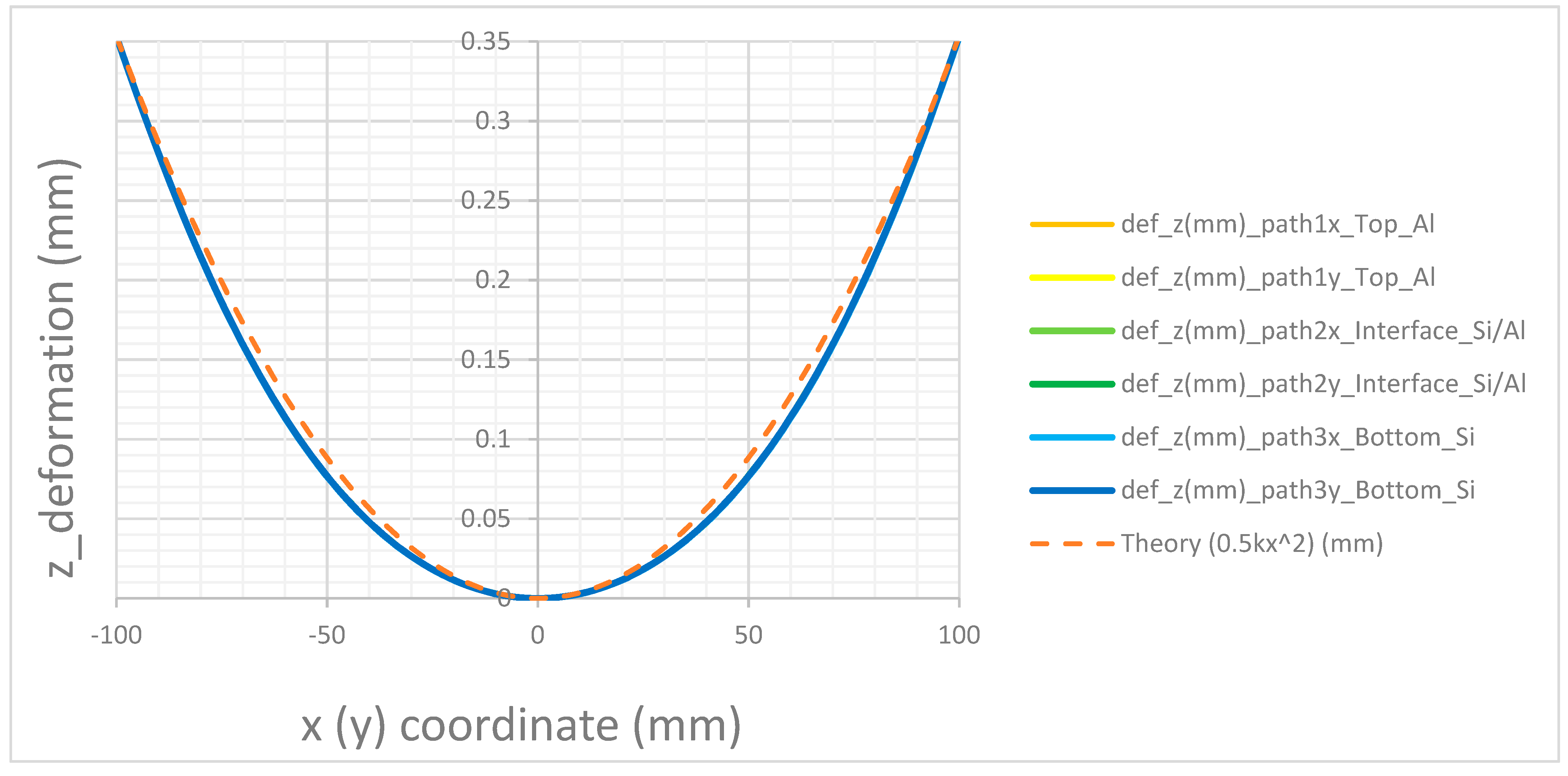
Figure 5 we report the directional deformation in the z direction for each pair of paths 1x, 1y, on the top of the metal layer, 2x, 2y, at the interface between the metal layer and the semiconductor, 3x and 3y, at the bottom of the central taiko semiconductor region, respectively, reported as a function of the coordinate x (y) along the path itself, for the case of the FSM-taiko wafer that is 200 μm thick. In general, we observed that for each pair of paths there is no difference in the curvatures in the x- and y-directions, confirming that the wafer has warped symmetrically. Moreover, all the paths provide the same deformation. The curvature at the center of the wafer has been determined from a parabolic approximation and the trend according to the theory reported for a comparison. We can observe as the parabolic trend fits well with the directional deformation of the taiko wafer.
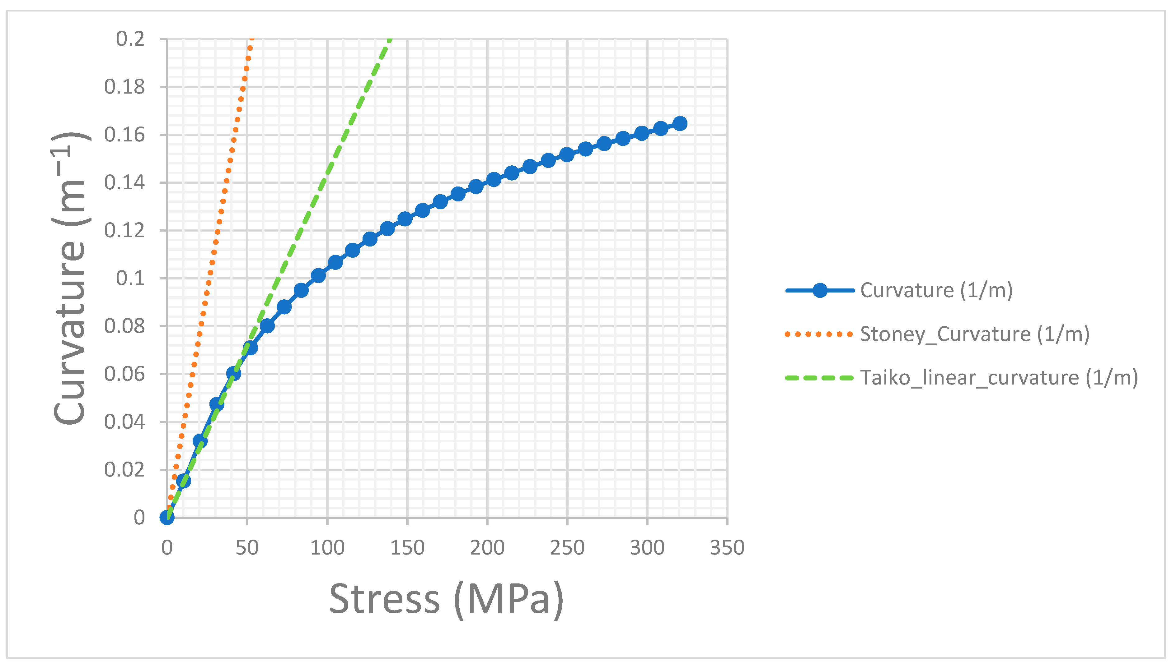
In
Figure 6 the curvature as a function of the stress (von Mises) for a taiko wafer having
hs = 200 µm and the other quantities fixed to the typical value reported in
Table 1 has been reported. In the graph, the line determined by the slope of the Stoney equation and the tangent line to the curvature vs. stress curve are shown. The slope, defined by the ratio
and hence the curvature of the taiko wafer, is lower with respect to the Stoney case.
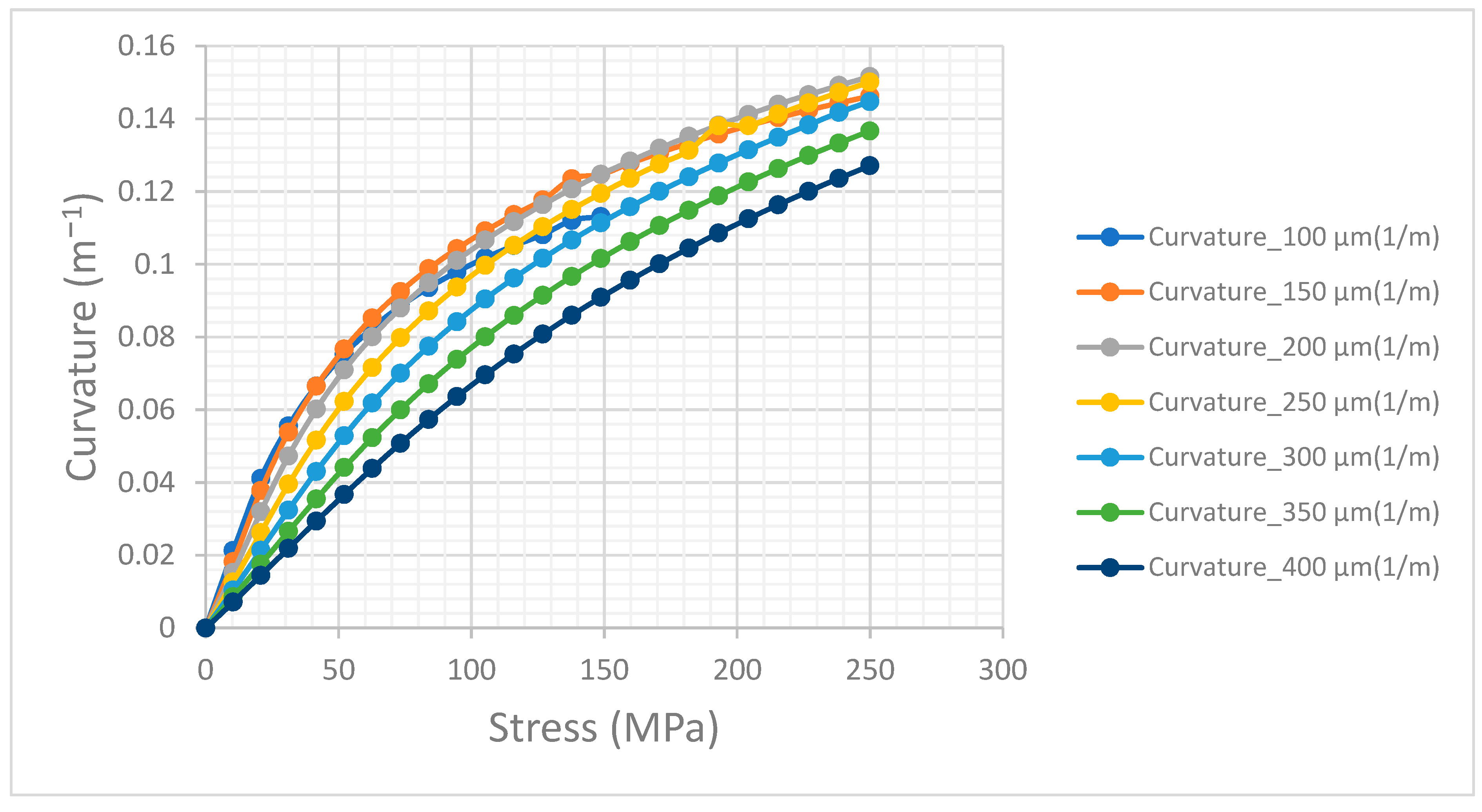
In
Figure 7 we report the curvature as a function of the stress for a set of seven taiko wafers having
hs ranging across the interval 100–400 µm and the other quantities fixed to the typical value reported in
Table 1. In particular, the height
was set to a constant value of 450 µm. For each
, we calculated the slope of the tangent line to the origin of the curve.
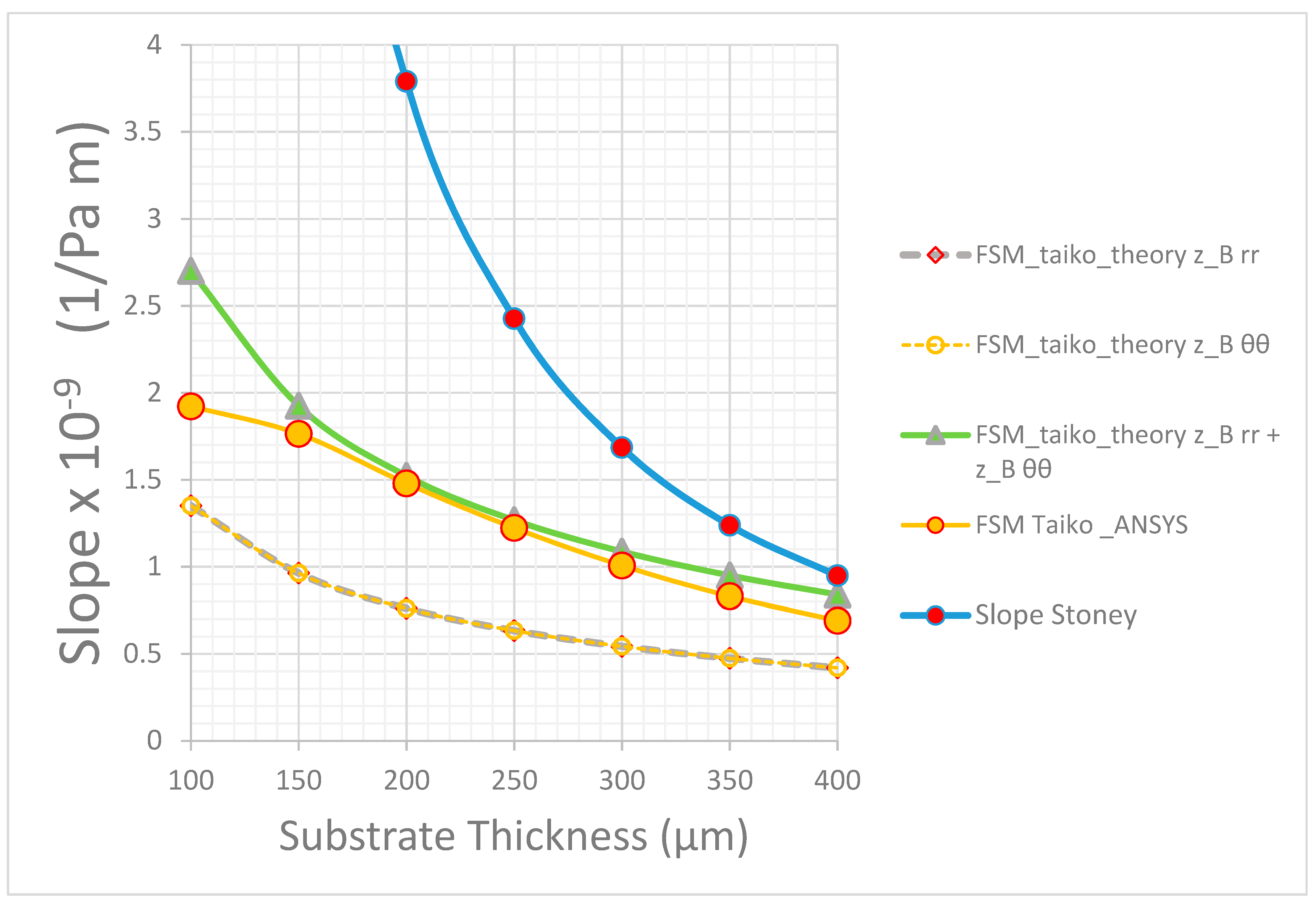
In
Figure 8, the values of these slopes (
) have been reported as a function of the thickness
of the substrate in the central region of the taiko wafer. For comparison, we also reported the slope determined by the Stoney equation for a flat wafer. As can be observed, the slope, and hence the curvature as a function of the stress, though increasing with the decrease in the thickness of the wafer, is lower with respect to the case of a flat substrate or a Stoney case, because of the mitigation effect determined by the taiko wafer. To complete our investigation on the FSM-taiko wafer we calculated the slope as a function of the thickness as provided by the analytical developments reported in the first part of this work, by Equations (26) and (34). The results have been compared with those provided by ANSYS and reported in the same
Figure 8. The values of the slopes resulting from the analytical calculations are practically the same; and hence there is one value for the
value. Moreover, though the calculated values are well below the value provided by ANSYS, it is possible to gain the order of magnitude of the slope and the trend. Finally, it is worth observing that by adding the two contributions of the slopes
and
, determined by the developed theory, a good agreement with the ANSYS simulation experiment was found. This indicated that the theory explains well the physics which is behind the mitigation of the warpage of a taiko wafer.
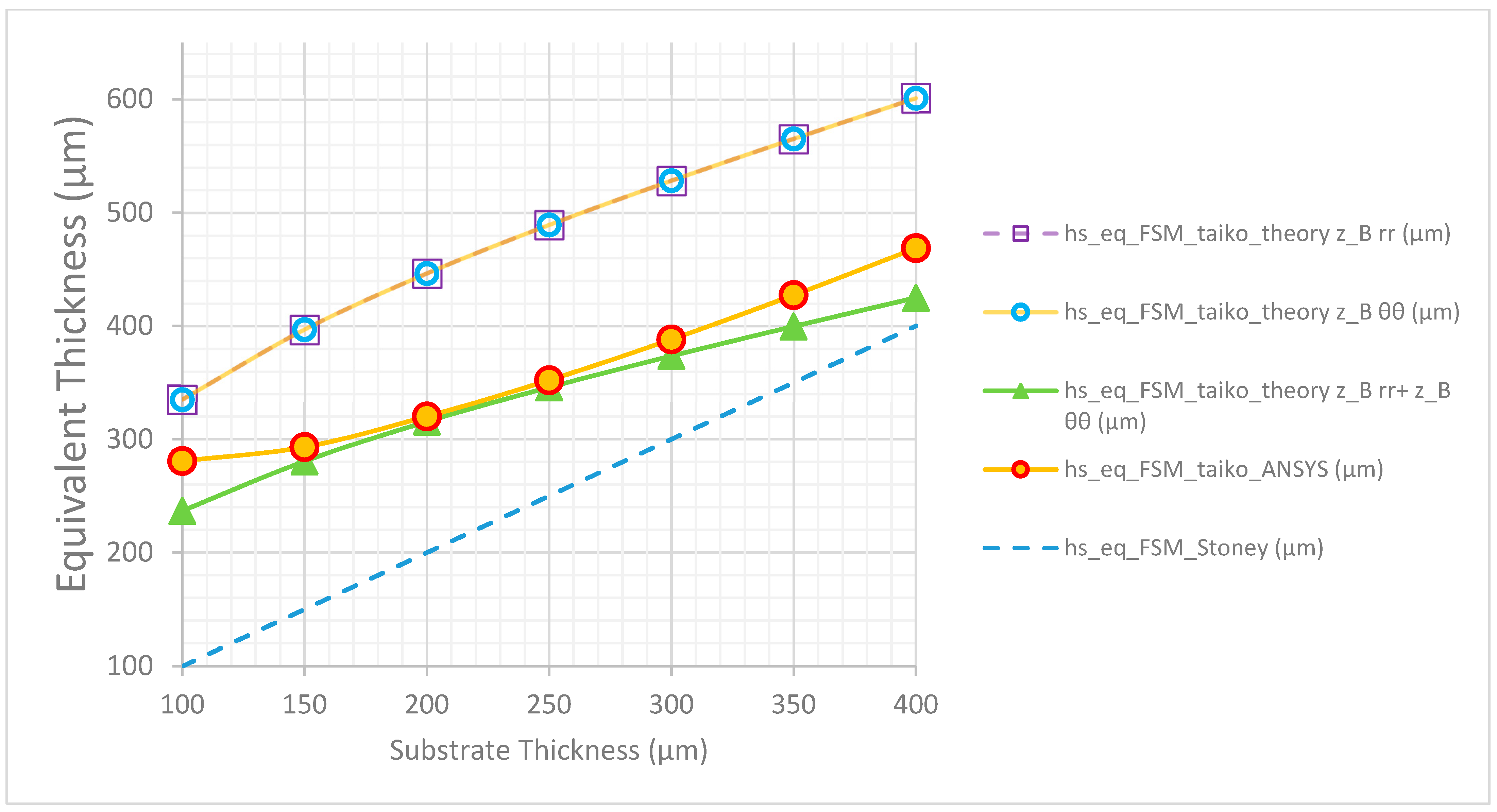
Lastly, in
Figure 9, we report the equivalent thickness calculated according to Equation (28), of the wafer as calculated from the theory and from the ANSYS results as a function of
hs. These results show that an FSM taiko wafer warps as an equivalent standard wafer whose substrate thickness is higher.
7. Conclusions
In conclusion, we have determined analytically, in a linear approximation, the dependence of the slope of the curvature vs. stress curve, of an FSM taiko wafer as a function of the thickness of the substrate. From this we derived the equation of the equivalent thickness of an FSM taiko wafer. In parallel, we developed an FEM ANSYS mechanical model of the same system and investigated the warpage as a function of the stress of the metal layer, for different values of substrate thickness. From these data we calculated the slope as a function of the thickness, as well as the values of the equivalent thickness and pursued a comparison with the analytical results.
The comparison of the two approaches reveals that the analytical solution provides the right order of magnitude of the slope and a value which agrees with the ANSYS simulations experiments. Moreover, the trend of the mitigation of the curvature due to the structure of the taiko wafer, by thinning the substrate, can be reproduced, also showing a good match with the finite element model devised with the ANSYS simulation tools. Hence, by exploiting simulations, it is proven that the FSM-taiko wafer behaves as an equivalent flat wafer whose thickness is higher than the substrate thickness in the central region of the taiko wafer. All these findings indicate that the theory explains well the physics which is behind the mitigation of the warpage of a taiko wafer. On the other hand, since the results obtained with ANSYS have been validated, we can rely on these simulation experiments to explore further properties of an FSM taiko wafer. Lastly the obtained results can also be extended to investigate other wide band gap semiconductors such as silicon carbide and gallium nitride.


