Article

Prediction of Microwave Characteristic Parameters Based on MMIC Gold Wire Bonding

School of Electronic and Information Engineering, Nanjing University of Information Science and Technology, Nanjing 210044, China
*
Author to whom correspondence should be addressed.
These authors contributed equally to this work.
Appl. Sci. 2023, 13(17), 9631; https://doi.org/10.3390/app13179631
Submission received: 13 July 2023 / Revised: 16 August 2023 / Accepted: 23 August 2023 / Published: 25 August 2023
(This article belongs to the Special Issue Device and Integration Technology of Microelectronics)

Abstract

:
In this paper, a method based on deep learning is proposed to predict the parameters of bonded metal wires, which solves the problem that the transmission characteristics of S-parameters cannot be predicted. In an X-band microwave chip circuit, gold wire bonding technology is often used to realize bonding interconnection, and the arch height and span of the bonded metal wire will have a great influence on the microwave transmission characteristics. By predicting the S-parameters of the bonded metal wire, the relationship between the structure parameters of the single wire and the transmission performance of the microwave device can be deduced. First, the gold wire bonding model is established in HFSS simulation software. After parameter optimization, the simulation results meet the requirements of establishing data sets. Then the sampling range of S parameters is set, and the parameters are scanned to establish data sets. Second, the artificial neural network model is built. The model adds a dropout mechanism to the hidden layer to enhance the generalization of the neural network, prevent overfitting phenomenon, and significantly improve the model’s prediction performance. Finally, the model predicts the corresponding relationship between the arch height and span of the bonding wire and the insertion loss, return loss and standing wave ratio. The mean square error of the test set is less than 0.8. The experimental results show that compared with the traditional process measurement method, this method can quickly and accurately infer whether the microwave characteristics of the bonded product are qualified, which greatly reduces the time and economic cost of the engineer and improves the work efficiency.

1. Introduction

Integrated circuits are an integral and important part of electronic products such as smartphones, computers, and robots [1,2,3]. The IC industry chain includes design, manufacturing, packaging, and testing, and packaging plays an important role in this field [4,5]. Gold wire bonding [6,7,8] is a special soldering technique that mainly uses gold wire to connect homogeneous or heterogeneous metals, semiconductors, plastics, and ceramics, and is widely used in semiconductor devices and integrated circuit packaging, which is the most versatile and simple and effective method.
In microwave chip circuits, each MMCM module has hundreds or even thousands of bonding wires to achieve interconnection between components [9]. X-band T/R components and other microwave multi-chip circuits often use gold wire bonding technology to achieve interconnection between a single microwave integrated circuit chip (MMIC) [10], an application-specific integrated circuit chip (ASIC) and other components. Figure 1 for the group’s laboratory design of a microwave multi-chip circuit products, the product internal chip through the bonding alloy wire and the substrate to achieve electrical interconnection, so as to achieve inter-chip information interoperability [11,12]. Each of these chips and modules, the microwave characteristics of each bonding alloy wire parameters may have an impact on the overall performance. The effect of interconnect wires on microwave transmission is weak and generally negligible in low frequency applications, but as the frequency increases, parameters such as the number of bonding alloy wires, length, arch height, span, and solder joint location, can have a serious impact on the microwave transmission characteristics [13,14,15]. Whether the span or the increase in arch height, will lead to an increase in loss, so that the standing wave ratio increases, the forward transmission coefficient decreases transmission performance decreases.
Bonding alloy wires are commonly used in the press-soldering process of low power devices and integrated circuit packages due to their advantages of high conductivity, corrosion resistance and good toughness [16]. In the semiconductor manufacturing industry, about one-third of all failures are caused by lead bonding, and the quality of lead bonding plays a very important role in ensuring the proper operation of electronic systems. Zhou et al. [17] introduced the development history of gold wire bonding wires, as well as the reliability and basic performance of interconnect wires under different materials. They also compared the application of interconnect wires under three different materials, and finally identified gold wires for interconnecting between chips. Thereafter, F. Alimenti et al. [18] proposed the use of finite difference method in time domain (FDTD) to analyze the electromagnetic properties of gold wire bonding. It is now widely used in the calculation of microwave three-dimensional structures, but it requires high computer performance and the calculation is time-consuming. Such methods include trial and error, tuning parameter optimization and parameter scanning, which is a long process [19]. Therefore, in order to solve similar problems and seek an efficient method, deep learning methods benefit us.
Currently, deep learning methods have been widely used in various fields. Machine learning has had an impressive impact on sensor data processing through embedded features such as robustness, resolution enhancement in measurement data points, and other applications for analyzing/optimizing sensor data [20]. Methods based on fully connected neural networks (FCNN) have achieved many results in prediction-related tasks [21]. Kao et al. [22] developed a deep learning-based fault diagnosis framework, which can detect the bonding head in the bonding line equipment and determine whether the bonding head is installed correctly to further reduce the cost. Wu and Chu [23] proposed a design method based on the integrated structure of chip packages, which showed that the Random Forest algorithm can predict the stresses of chip design. Jin et al. [24] predicted the radiated electric field in bonding wire packages by deep learning methods, optimizing the model parameters to reduce the prediction error. Although many scholars optimized and predicted the model parameters by deep learning methods, fewer scholars studied the microwave transmission characteristics by the arch height and span of the gold wire bonding interconnect wires in the field of integrated circuit packaging. Compared with the traditional model structure, this paper designed a capacitive compensation structure, where the chip is connected to the microstrip line through the gold wire bonding interconnect wires, which improves the microwave transmission characteristics. At the same time, the gold wire bonding technology used in the gold wire becomes thinner and thinner, the bonding arch height decreases, the bonding span decreases, the number of bonding alloy wires in the chip increases, and the complexity of the traditional measurement of the microwave transmission characteristics of bonding alloy wires increases, so that this hinders the rapid development of the encapsulation technology.
In this paper, we propose a deep learning-based method to achieve the prediction of bonding alloy wire parameters. Through an artificial neural network model built independently, the correspondence between the arch height and span of the bonding alloy wire and the insertion loss, return loss and standing wave ratio is predicted, and compared with previous studies, the method can quickly and accurately deduce whether the microwave characteristics of the bonded products are qualified, which greatly reduces the time and economic cost of engineers, improves the efficiency, and lays a solid technical and theoretical foundation for higher frequency research.
To verify the effectiveness of our proposed method, we scanned the S-parameters, obtained a relatively large amount of data, and conducted extensive experiments on the dataset. The experimental results show that our proposed prediction method is faster and more accurate than the previous tested methods. This paper is organized as follows: Section 2 introduces the model and relevant data for this experiment. Section 3 presents our proposed method. Section 4 outlines the experimental results and analyzes them.
In summary, this work has made the following contributions:
1.
Construction of a model for gold wire bonding and continuous optimization of this model for data set acquisition and comparison of prediction results;
2.
Designing a fully connected neural network model with a prediction accuracy generally better than the conventional model for the prediction of microwave transmission characteristics;
3.
The experimental results show that our method achieves fast and accurate prediction compared with the simulation results of the model.

2. Model and Analysis

In this paper, we construct a gold wire bonding model in HFSS software, and optimize the S-parameter, which greatly improves the microwave transmission characteristics.

2.1. Construction of Gold Wire Bonding Model

Figure 2 shows a schematic diagram of the structure model of a gold wire bonding interconnection line. The gold wire bonding model is established by HFSS simulation software, which is connected between the chip and T-type microstrip line by a single gold wire interconnection line, the arch height of the bonding alloy wire is h, the span is l, the microstrip line width is w. The substrate material at the bottom of the model consists of a double-sided copper-clad plate (Rogers 4350) with a relative dielectric constant of 3.66 and a loss angle tangent value of 0.004. The small square that fits tightly the chip material is nickel-plated and gold-plated (Mo80Cu20), the T-shaped microstrip material is copper, the bottoms of the first two materials are coated with copper, the thickness is 0.035 mm, the middle interconnected gold wire material is gold. For the accuracy of the post-test, the encapsulation environment uses nitrogen (N2) environment. The six geometric parameters we designed are the arch height h, span l, and microstrip line width w of the bonding alloy wire, which are numbered as w1, w2, w3, and w4 in the order from left to right. Figure 2 shows two ports, port 1 and port 2. Port 1 is connected to the microstrip line 4, the bonding alloy wire is connected to the chip at port 2, and both port excitations are 50 ohms.

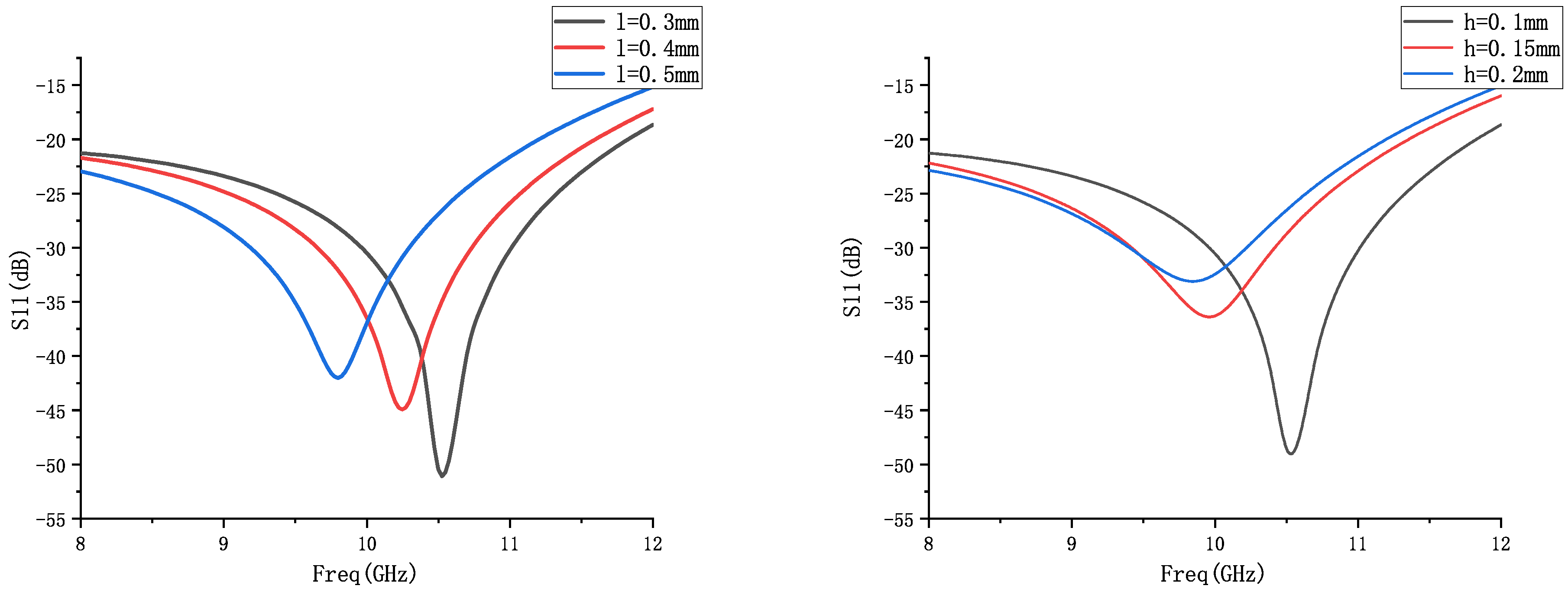
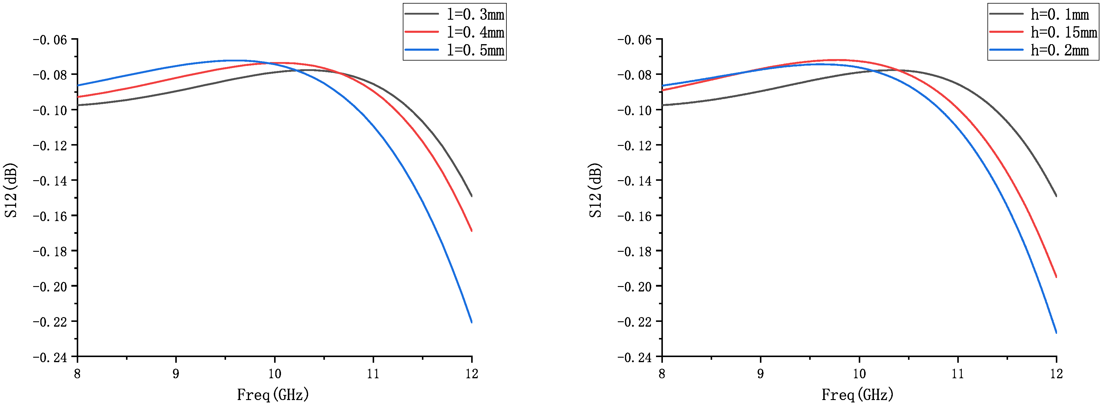
2.2. Simulation Results and Analysis

The return loss is the ratio between the energy lost due to the reflection of the signal in the transmission process and the energy of the input signal [25]. A comparison of the return loss simulation results is shown in Figure 3 below. This conclusion can be obtained from the comparison result graph: as the arch height and span increase, the resonance point is shifted to the lower frequency, and the return loss is below −15 dB in the X-band (8–12 GHz), and at the resonance point near the center frequency of 10 GHz, it reaches −52 dB, which indicates a good matching performance.
Insertion loss is the ratio of the output signal to the input signal, the larger the value, the smaller the transmission loss of the signal and the better the electromagnetic shielding effect [26]. A comparison of the insertion loss simulation results is shown in Figure 4 below. The conclusion can be obtained from the comparison result graph: with the increase in arch height and span, the loss increases gradually, especially in 10–12 GHz is more obvious, but its microwave transmission characteristics still meet the design requirements, and at the resonance point near the center frequency of 10 GHz, it reaches −0.07 dB.
The closer the VSWR is to 1 indicates that most of the energy is transmitted to the T-match network through our designed gold filament, and only a small portion of the energy stays in the chip in the form of standing waves [27]. The VSWR comparison results are schematically shown in Figure 5 below: with the increase in arch height and span, the VSWR is better than 1.45 dB throughout the X-band (8–12 GHz), in the close to the center frequency of 10 GHz At the resonance point near the center frequency of 10 GHz, it is even closer to 1.05 dB, which is an excellent performance.
Bonded wire interconnect circuit is a two-port reciprocal network, according to the microwave network theory can be obtained from the conclusion: S11 = S22, S12 = S21, there are different cases, in high-speed circuit design used in microstrip line or ribbon line, have a reference plane, for the asymmetric structure (but the parallel two-conductor line is a symmetric structure), so the S11 is not equal to the S22, but to meet the conditions of reciprocity, there is always S12 = S21 [28]. The simulation results of the S parameters of the gold wire bonding network model built in this experiment are relatively satisfactory, on this basis, we need to establish the data set, in order to make the study more feasible, we need to carry out boundary constraints on the geometric parameters, and then carry out parameter scanning on the S parameters to establish the data set to provide data support for the artificial neural network model built subsequently, the range of variation in each design parameter is shown in Table 1 below:
In the X-band, each design parameter is restricted to the parameter range, and the parameter simulation is performed within this range. The S-parameters obtained from the simulation are sampled at equal intervals with an interval of 0.1 GHz, and the sampling points of each data set are 41, and the sampling points of the three data sets are 123 in total, and a total of 39375 pairs of data are obtained, and the data set is established. The three sets of data are S11, S12, and VSWR. S11 [29] in the literature indicates the return loss, S12 [30] in the literature indicates the insertion loss, and VSWR [31] in the literature indicates the standing wave ratio.

3. Model and Analysis

In this paper, we build a neural network model, which belongs to a classical regression model. The three sets of data sets are trained and predicted in the same model, and the dropout mechanism is added to the last hidden layer to enhance the generalization of the neural network, prevent overfitting phenomenon, and greatly improve the work efficiency and prediction performance. The results obtained by the neural network model belong to a specific type of substrate, the number of input and output layers are set by themselves according to the experimental needs, the arch height and span of the gold wire bonding and the microstrip line width have a great influence on the microwave transmission characteristics of the S-parameter, so the number of input layers is set to be 6, and the output layer is set to be 123, and the hidden layer needs to be constantly fine-tuned to optimize the neural network model, and the activation function has a certain influence on the performance of the neural network model, and the number of neurons needs to be repeatedly experimented to determine the neuron counts. Although the number of neuron layers and the activation function may not be the optimal choice, the results obtained from its constructed neural network model are in line with the expected results.

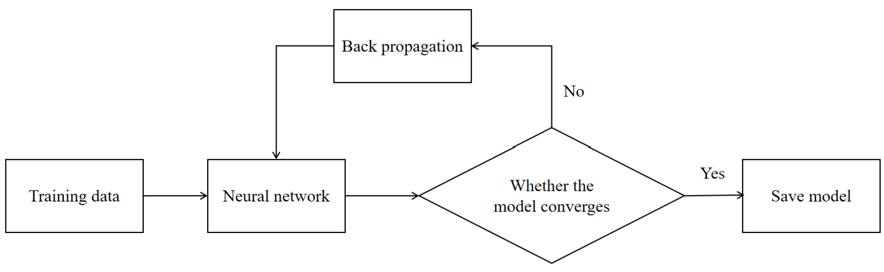
3.1. Building an Artificial Neural Network

Neural networks, or artificial neural networks, are an algorithmic system developed by humans inspired by the structure of biological nerve cells [32]. The advantage of neural networks is that they can be built according to the constructed model, supervised continuous learning, and the flow diagram of the autonomously built artificial neural network model is shown in Figure 6:
The number of neurons in the input layer is 6, and the number of neurons in the output layer is 123, including 6 hidden layers. The number of neurons and activation function of each layer are shown in Table 2: Among them, the neurons are numbered h1–h6 from left to right, BN is Batch Normalization, which normalizes the value of the input activation function in the hidden layer and enables the data to be mapped to a reasonable interval without changing the data distribution characteristics. This makes the gradient training of hidden layer energy more stable during backpropagation and helps prevent overfitting of the neural network. Another way to prevent the neural network from overfitting is to introduce the Dropout mechanism. That is, for the hidden layer training, the internal neurons do not adopt the form of full connection with the next layer, but will randomly drop some of them, thus enhancing the generalization of the neural network and preventing overfitting.
The initial learning rate is set to 0.0001, and the optimizer selects the adaptive optimizer Adam. This is an optimization function that automatically adjusts the learning rate according to the training process, which is more computationally efficient and less memory-demanding than other optimizers and generally does not require artificial parameter adjustments or just fine-tuning of the learning rate during the training process, which is very suitable for most of the application scenarios, especially those where the optimization objective is not known. MSE reflects the mathematical expectation of the square of the difference between the predicted value and the true value of the model. R-square indicates the degree of fit between the predicted value and the true value, and the value is between 0 and 1. The closer the R-square is to 1, the better the model fit is [33]. The formula for each evaluation index is shown below.
M A E = 1 m i = 1 m y i y ^ i
R M S E = 1 m i = 1 m y i y ^ i 2
R 2 = 1 i 1 m y i y ^ i 2 i = 1 m y i y ¯ 2
M S E = 1 m i = 1 m y i y ^ i 2
Equation (4) where m is the number of samples, y i and y ^ i are the true and predicted values of the ith sample, respectively, and y ¯ is the average of the true values of the m samples. We choose the mean square error (MSE) as the loss function to characterize the spatial distance between the model output results and the actual labels, and the optimization goal is to train the neural network by reducing this spatial distance as much as possible. For network training, the dataset is randomly divided in the ratio of 1:9, where 1 becomes the test set and 9 becomes the training set. The data in the training set will be involved in the training of the neural network so that the neural network back propagates to learn the data features, and the test set data will not be involved in the neural network training. Before the neural network model starts training, an initial assignment of the parameters within the network model weights, which is relatively small, is required so that the starting values of the repeatedly trained networks do not differ much and play a positive role in evaluating the different parameters for the training of the network model. During the training process of the neural network model, the model is not unique considering that the neural network has the property of infinite approximation. When the network training reaches a certain level, the test set data is input to the network for model evaluation, and when the test set data works well, the model can be considered to reach the convergence condition, terminate the training and save the network training model. The schematic diagram of the whole neural network training process is shown in Figure 7.
At the early stage of model training, the convergence of the model is judged by the change of the loss value, and when the loss curve appears to be divergent or repeatedly turbulent, the model is judged to be non-convergent and adjustments need to be made to the model.
In this experiment, three sets of data are trained under the same model, and the loss function curve is shown in Figure 8 for 1000 iterations in order to reduce the error. In this experiment, when the model was first trained, the loss function value tended to decline in a straight line, then the speed slowed down, and eventually the speed leveled off and converged near a tiny value. From the training and prediction loss function values, the error was small, and we set the variance threshold to 1.5. When the variance value was less than 1.5, the network was judged to be accurate in prediction, and vice versa. We selected 1300 sets of data in the test set, and 1274 sets of data met the prediction readiness, with an accuracy rate of 98%, at which time we considered that the network training reached the convergence state, terminated the network training and saved the network training model.

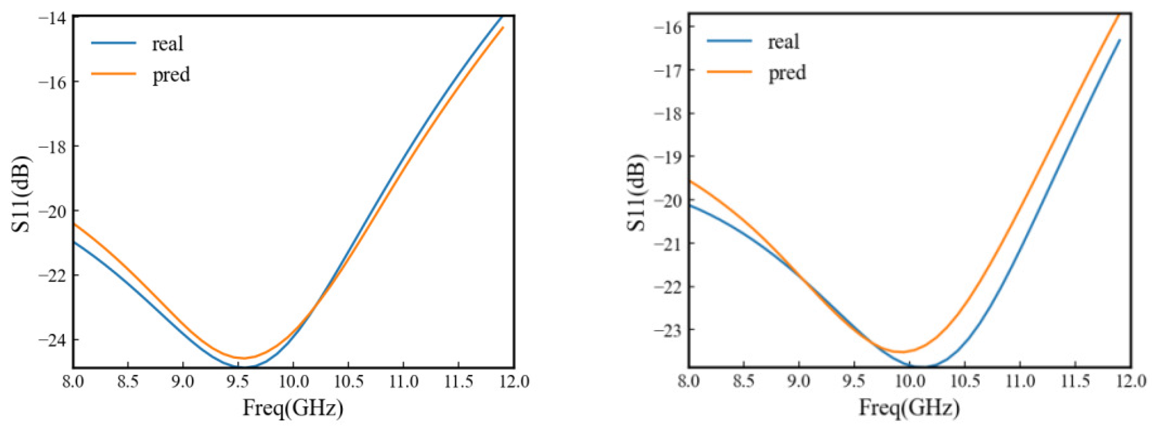
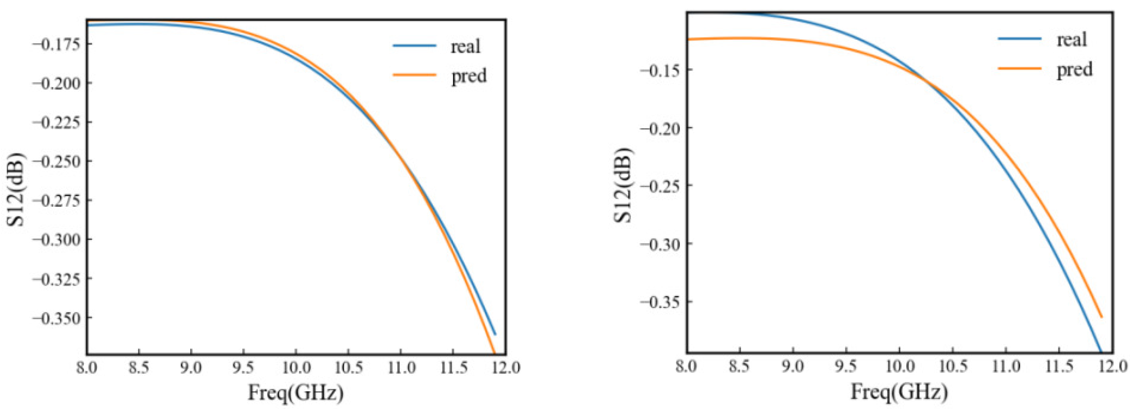
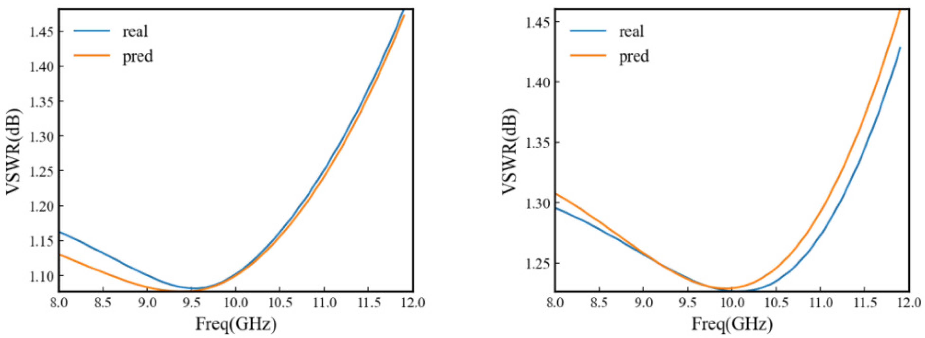
3.2. Experimental Results and Analysis

The experiments show that in the X-band, at the resonance point near the center frequency of 10 GHz, inputting the value 52 into the neural network model, the simulation and prediction results of return loss in figure (left) are both close to −25 dB, and the average error between them is within 0.2 dB, inputting the value 674 into the neural network model, the simulation and prediction results of return loss in figure (right) are both close to −24 dB, and the average error between them is within 0.3 dB. The prediction results of the return loss neural network are shown in Figure 9.
Experiments show that in the X-band, at the resonance point near the center frequency of 10 GHz inputting the value 193 into the neural network model, the simulation and prediction results of insertion loss in figure (left) are both close to −0.2 dB, and the average error between them is within 0.05 dB, inputting the value 682 into the neural network model, the simulation and prediction results of insertion loss in figure (right) are both close to −0.16 dB, and the average error between them is within 0.1 dB and the insertion loss neural network prediction. The results are shown in Figure 10 below.
The experiments show that in the X-band, at the resonance point near the center frequency of 10 GHz, inputting the value 86 into the neural network model, the simulation and prediction results of VSWR in figure (left) are both close to 1.08 dB, and the average error between them is within 0.02 dB, inputting the value 678 into the neural network model, the simulation and prediction results of return loss in figure (right) are both close to 1.22 dB, and the average error between them is within 0.1 dB. The prediction results of VSWR neural network are as follows Figure 11 shows.
As can be seen from Figure 9, Figure 10 and Figure 11 above, the neural network learns the microwave transmission characteristics of the S-parameters of a single wire bonded interconnect line, and can accurately predict the correspondence between the arch height and span of the interconnected wire as well as the insertion loss, return loss, and VSWR. The entire neural network model takes some time to train, and the neural network model can predict the data in a flash after completing the training, while the electromagnetic simulation takes a lot of time under the same conditions. The simulation results are not that much different from the prediction results. Additionally, this model can also study the microwave transmission characteristics under any parameters of the structure by just imputing the data into the neural network model we designed and the microwave transmission characteristics under the corresponding parameters will be obtained.

4. Conclusions

In this paper, an artificial neural network model is built based on a deep learning approach to achieve the prediction of microwave transmission characteristics of S-parameters of single gold wire bonded interconnects. The experiments show that the prediction error is small, and the mean square error of the test set is less than 0.8, which is within the acceptable range. It can be seen that the prediction results of the artificial neural network model proposed in this paper have high accuracy, and it is feasible to apply the deep learning approach to the S-parameter prediction of bonded alloy wires. Future work will produce and measure the physical objects and analyze the physical measurement results with the predicted data.

Author Contributions

Conceptualization, S.Y.; methodology, S.Y. and H.L.; software, H.L; valida-tion, S.Y. and H.L.; resources, S.Y.; supervision, S.Y. All authors have read and agreed to the published version of the manuscript.

Funding

This research received no external funding.

Institutional Review Board Statement

Not applicable.

Informed Consent Statement

Not applicable.

Data Availability Statement

Not applicable.

Conflicts of Interest

The authors declare no conflict of interest.

References

  1. Shi, J.; Liu, S.; Zhang, L.; Yang, B.; Shu, L.; Yang, Y.; Ren, M.; Wang, Y.; Chen, J.; Chen, W.; et al. Smart textile-integrated microelectronic systems for wearable applications. Adv. Mater. 2020, 32, 1901958. [Google Scholar]
  2. Park, J.; Kim, J.; Kim, S.Y.; Cheong, W.H.; Jang, J.; Park, Y.G.; Na, K.; Kim, Y.T.; Heo, J.H.; Lee, C.Y.; et al. Soft, smart contact lenses with integrations of wireless circuits, glucose sensors, and displays. Sci. Adv. 2018, 4, eaap9841. [Google Scholar] [CrossRef] [PubMed]
  3. Heck, M.J.; Bauters, J.F.; Davenport, M.L.; Doylend, J.K.; Jain, S.; Kurczveil, G.; Srinivasan, S.; Tang, Y.; Bowers, J.E. Hybrid silicon photonic integrated circuit technology. IEEE J. Sel. Top. Quantum Electron. 2012, 19, 6100117. [Google Scholar] [CrossRef]
  4. Tu, K.N.; Liu, Y. Recent advances on kinetic analysis of solder joint reactions in 3D IC packaging technology. Mater. Sci. Eng. R Rep. 2019, 136, 1–12. [Google Scholar]
  5. Aryan, P.; Sampath, S.; Sohn, H. An overview of non-destructive testing methods for integrated circuit packaging inspection. Sensors 2018, 18, 1981. [Google Scholar] [CrossRef]
  6. Zhan, D.; Lin, J.; Yang, X.; Huang, R.; Yi, K.; Liu, M.; Zheng, H.; Xiong, J.; Cai, N.; Wang, H.; et al. A Lightweight Method for Detecting IC Wire Bonding Defects in X-ray Images. Micromachines 2023, 14, 1119. [Google Scholar] [CrossRef] [PubMed]
  7. Tsai, T.N. A hybrid intelligent approach for optimizing the fine-pitch copper wire bonding process with multiple quality characteristics in IC assembly. J. Intell. Manuf. 2014, 25, 177–192. [Google Scholar]
  8. Wang, C.; Sun, R. The quality test of wire bonding. Mod. Appl. Sci. 2009, 3, 50–56. [Google Scholar] [CrossRef]
  9. Das, R.N.; Bolkhovsky, V.; Tolpygo, S.K.; Gouker, P.; Johnson, L.M.; Dauler, E.A.; Gouker, M.A. Large scale cryogenic integration approach for superconducting high-performance computing. In Proceedings of the 2017 IEEE 67th Electronic Components and Technology Conference (ECTC), Lake Buena Vista, FL, USA, 30 May–2 June 2017; IEEE: Piscataway Township, NJ, USA, 2017; pp. 675–683. [Google Scholar]
  10. Wu, P.; Yu, Z.; Liu, K.; Zhan, F.; Wang, S.; Wang, K.; Hao, C. Low-Profile and High-Integration Phased Array Antenna Technology. In Proceedings of the 2022 IEEE Conference on Antenna Measurements and Applications (CAMA), Guangzhou, China, 14–17 November 2022; IEEE: Piscataway Township, NJ, USA, 2022; pp. 1–6. [Google Scholar]
  11. Zhang, S.; Li, Z.; Zhou, H.; Li, R.; Wang, S.; Paik, K.W.; He, P. Recent Prospectives and Challenges of 3D Heterogeneous Integration. e-Prime-Adv. Electr. Eng. Electron. Energy 2022, 2, 100052. [Google Scholar]
  12. Lu, J.; Wang, W.; Wang, X.; Guo, Y. Active Array Antennas for High Resolution Microwave Imaging Radar; Springer Nature: Berlin/Heidelberg, Germany, 2023. [Google Scholar]
  13. Béjanin, J.; McConkey, T.; Rinehart, J.; Earnest, C.; McRae, C.; Shiri, D.; Bateman, J.; Rohanizadegan, Y.; Penava, B.; Breul, P.; et al. Three-dimensional wiring for extensible quantum computing: The quantum socket. Phys. Rev. Appl. 2016, 6, 044010. [Google Scholar] [CrossRef]
  14. Zhang, H.; Lan, Y.; Qiu, S.; Min, S.; Jang, H.; Park, J.; Gong, S.; Ma, Z. Flexible and stretchable microwave electronics: Past, present, and future perspective. Adv. Mater. Technol. 2021, 6, 2000759. [Google Scholar] [CrossRef]
  15. Kiang, J.F.; Chung, S.J.; Chen, H.H. Electrical Packaging for Microwave and Millimeter Wave Circuits. In Novel Technologies for Microwave and Millimeter—Wave Applications; Springer: Berlin/Heidelberg, Germany, 2004; pp. 545–562. [Google Scholar]
  16. Zhou, H.; Zhang, Y.; Cao, J.; Su, C.; Li, C.; Chang, A.; An, B. Research Progress on Bonding Wire for Microelectronic Packaging. Micromachines 2023, 14, 432. [Google Scholar] [PubMed]
  17. Li, J.; Wang, J.; Yi, X.; Liu, Z.; Wei, T.; Yan, J.; Xue, B.; Li, J.; Wang, J.; Yi, X.; et al. Packaging of Group-III Nitride LED. In III-Nitrides Light Emitting Diodes: Technology and Applications; Springer: Berlin/Heidelberg, Germany, 2020; pp. 185–202. [Google Scholar]
  18. Wang, T.; Harrington, R.F.; Mautz, J.R. Quasi-static analysis of a microstrip via through a hole in a ground plane. IEEE Trans. Microw. Theory Tech. 1988, 36, 1008–1013. [Google Scholar] [CrossRef]
  19. Pérez-Escribano, M.; Márquez-Segura, E. Parameters characterization of dielectric materials samples in microwave and millimeter-wave bands. IEEE Trans. Microw. Theory Tech. 2021, 69, 1723–1732. [Google Scholar] [CrossRef]
  20. Abdolrazzaghi, M.; Kazemi, N.; Nayyeri, V.; Martin, F. AI-Assisted Ultra-High-Sensitivity/Resolution Active-Coupled CSRR-Based Sensor with Embedded Selectivity. Sensors 2023, 23, 6236. [Google Scholar] [CrossRef]
  21. Li, J.; Wu, W.; Xue, D.; Gao, P. Multi-source deep transfer neural network algorithm. Sensors 2019, 19, 3992. [Google Scholar] [CrossRef] [PubMed]
  22. Kao, S.X.; Chien, C.F. Deep Learning Based Positioning Error Fault Diagnosis of Wire Bonding Equipment and an Empirical Study for IC Packaging. IEEE Trans. Semicond. Manuf. 2023. [Google Scholar] [CrossRef]
  23. Wu, H.; Chu, W. Machine learning assisted structural design optimization for flip chip packages. In Proceedings of the 2021 6th International Conference on Integrated Circuits and Microsystems (ICICM), Nanjing, China, 22–24 October 2021; IEEE: Piscataway Township, NJ, USA, 2021; pp. 132–136. [Google Scholar]
  24. Jin, H.; Gu, Z.M.; Tao, T.M.; Li, E. Hierarchical attention-based machine learning model for radiation prediction of wb-bga package. IEEE Trans. Electromagn. Compat. 2021, 63, 1972–1980. [Google Scholar] [CrossRef]
  25. Ahmed, O.; Thaher, R.H.; Ahmed, S.R. Design and fabrication of UWB microstrip Antenna on different substrates for wireless Communication system. In Proceedings of the 2022 International Congress on Human-Computer Interaction, Optimization and Robotic Applications (HORA), Ankara, Turkey, 9–11 June 2022; IEEE: Piscataway Township, NJ, USA, 2022; pp. 1–4. [Google Scholar]
  26. Saleh, S.; Ismail, W.; Abidin, I.S.Z.; Jamaluddin, M.H. 5G hairpin and interdigital bandpass filters. Int. J. Integr. Eng. 2020, 12, 71–79. [Google Scholar] [CrossRef]
  27. Zhao, Q.; Zhu, Q.; Yang, P.; Zhang, Z.; Luo, X.; Yan, Z. An Antenna Design of GNSS Terminal on B3 Frequency. In Proceedings of the 2023 2nd International Conference on Big Data, Information and Computer Network (BDICN), Xishuangbanna, China, 6–8 January 2023; IEEE: Piscataway Township, NJ, USA, 2023; pp. 130–133. [Google Scholar]
  28. Loracher, S.; Blau, K.; Stehr, U.; Stephan, R.; Hein, M. Experimental proof-of-principle of a passive, nearly reciprocal, transistor-based tuneable RF inductance. In Proceedings of the 2016 46th European Microwave Conference (EuMC), London, UK, 4–6 October 2016; IEEE: Piscataway Township, NJ, USA, 2016; pp. 1055–1058. [Google Scholar]
  29. Nikolaou, S.; Davidovic, M.; Nikolić, M.; Vryonides, P. Resonator type and positioning study for the creation of a potentially reconfigurable frequency notch in a UWB antenna return loss. In Proceedings of the 5th European Conference on Antennas and Propagation (EUCAP), Rome, Italy, 11–15 April 2011; IEEE: Piscataway Township, NJ, USA, 2011; pp. 350–353. [Google Scholar]
  30. Belevitch, V. Topics in the design of insertion loss filters. IRE Trans. Circuit Theory 1955, 2, 337–346. [Google Scholar] [CrossRef]
  31. Rizk, M.R.; Abou-Bakr, E.; Nasser, A.; El-Badawy, E.S.A.; Mahros, A.M. On the investigation of voltage standing wave ratio to design a low noise wideband microwave amplifier. In Proceedings of the 2016 Eighth International Conference on Ubiquitous and Future Networks (ICUFN), Vienna, Austria, 5–8 July 2016; IEEE: Piscataway Township, NJ, USA, 2016; pp. 568–572. [Google Scholar]
  32. Prieto, A.; Prieto, B.; Ortigosa, E.M.; Ros, E.; Pelayo, F.; Ortega, J.; Rojas, I. Neural networks: An overview of early research, current frameworks and new challenges. Neurocomputing 2016, 214, 242–268. [Google Scholar]
  33. Picard, R.R.; Cook, R.D. Cross-validation of regression models. J. Am. Stat. Assoc. 1984, 79, 575–583. [Google Scholar] [CrossRef]
Figure 1. Microwave multi-chip circuit.
Applsci 13 09631 g001
Figure 2. Diagram of the structural model of wire bonding interconnect. They should be listed as: (above) A top view of the model. (below) A section view of the model.
Applsci 13 09631 g002
Figure 3. Comparison of simulation results of return loss of bonded alloy wires under different arch heights and spans, they should be listed as: (left) Comparison of simulation results of return loss of bonded alloy wires with different spans schematic diagrams. (right) Comparison of simulation results of return loss of bonded alloy wires with different arch heights schematic diagram.
Applsci 13 09631 g003
Figure 4. Comparison of the simulation results of insertion loss of bonded alloy wires under different arch heights and spans, they should be listed as: (left) Comparison of simulation results of insertion loss of bonding alloy wires in different spans. (right) Comparison of simulation results of insertion loss of bonding alloy wires under different arch heights schematic diagram.
Applsci 13 09631 g004
Figure 5. Comparison of simulation results of VSWR of bonded alloy wires under different arch heights and spans, they should be listed as: (left) Comparison of VSWR simulation results of bonded alloy wires with different spans schematic diagram. (right) Comparison of simulation results of VSWR of bonded alloy wires with different arch heights.
Applsci 13 09631 g005
Figure 6. Schematic diagram of the process of the artificial neural network model.
Applsci 13 09631 g006
Figure 7. Model flow diagram.
Applsci 13 09631 g007
Figure 8. Schematic diagram of loss function curve.
Applsci 13 09631 g008
Figure 9. Diagram of the prediction result of echo loss neural network, they should be listed as: (left) The result of the first random draw. (right) The result of the second random selection.
Applsci 13 09631 g009
Figure 10. Insertion loss neural network prediction results schematic, they should be listed as: (left) The result of the first random draw. (right) The result of the second random selection.
Applsci 13 09631 g010
Figure 11. Schematic diagram of VSWR neural network prediction results, they should be listed as: (left) The result of the first random draw. (right) The result of the second random selection.
Applsci 13 09631 g011
Table 1. Table of design parameters distribution for the structural model of wire bonding interconnect.
Parameter Namehlw1w2w3w4
Minimum value0.1 mm0.3 mm1.841 mm0.192 mm1.593 mm0.267 mm
Maximum value0.2 mm0.6 mm2.241 mm0.392 mm1.993 mm0.667 mm
Spacing0.05 mm0.05 mm0.1 mm0.05 mm0.1 mm0.1 mm
Table 2. Table of neural network structure parameter.
NameInputh1h2h3h4h5h6Output
Number of neurons62050100400400200123
Activation functionReLUReLUReLUReLUReLUReLUReLU×
BN××××
Dropout×××××××
Disclaimer/Publisher’s Note: The statements, opinions and data contained in all publications are solely those of the individual author(s) and contributor(s) and not of MDPI and/or the editor(s). MDPI and/or the editor(s) disclaim responsibility for any injury to people or property resulting from any ideas, methods, instructions or products referred to in the content.

