Article

Optimization of Data Acquisition System Based on Electrical Impedance Tomography in Dredging Engineering

School of Electrical and Information Engineering, Tianjin University, Tianjin 300072, China
*
Author to whom correspondence should be addressed.
Appl. Sci. 2023, 13(17), 9931; https://doi.org/10.3390/app13179931
Submission received: 22 August 2023 / Revised: 25 August 2023 / Accepted: 31 August 2023 / Published: 2 September 2023
(This article belongs to the Special Issue Advanced Electronics and Digital Signal Processing)

Abstract

:
Electrical impedance tomography (EIT) is an advanced visualization detection technique with non-invasive, radiationless, and fast-response characteristics. As an important means in dredging engineering, EIT-based measurement can realize the estimate and computation of key flow parameters such as the flow velocity and solid phase fraction of solid-liquid two-phase flow in a pipe. Despite progress, both the data acquisition rate and the signal-to-noise ratio (SNR) of the existing EIT system are too low to meet many practical requirements. In this study, efforts are made concerning the EIT acquisition system by optimizing the sensor array, data acquisition system, and data communication module. Experimental results show that (1) the optimized system has an SNR of 73 dB, which is about 40% higher than the original system, and (2) the optimization of data transmission methods can achieve a maximum allowable transmission rate of 316.4 Mbps, sufficient to support data transmission over 1000 frames per second. Consequently, the key problems of the existing EIT acquisition system are substantially overcome.

1. Introduction

Electrical impedance tomography (EIT) is an advanced detection technique that solves electrical parameter distribution over all pixels in a detection field [1]. By measuring the electrical signals at the field’s boundaries, the target objects within the measured field can be visually reconstructed by various pixel greyscales. Since EIT has advantages, such as its radiationless, non-invasiveness, fast response, and low cost, it has received increasing attention in many important applications [2].
The data acquisition system plays an important role in the EIT detection process. The earliest acquisition system is a single row of 16 electrode sensors called Sheffield Mark I [3]. The excitation frequency of the system is 50 kHz, and the data acquisition frame rate is 12.5 fps. Later, Mark II and Mark 3.5a were developed based on this system, and the new system achieved a signal-to-noise ratio (SNR) of 55 dB [4,5]. Holder et al. designed a multi-frequency excitation system with excitation frequencies ranging from 225 Hz to 65 kHz based on the Mark I system, which aimed to design brain imaging for changes in electrical impedance during brain activity [6]. Ryan et al. presented a set of EIT systems for detecting breast cancer, with a digital signal process (DSP) as the core master component of the system [7]. Harsh et al. conducted the Kyung Hee University (KHU) Mark 2.5 multi-frequency EIT system, which modified the central control unit to a field programmable gate array (FPGA) [8]. The proposal of the new scheme optimized the digital design after greatly reducing system artifacts and maximizing system performance.
Recently, the research group attached to Tianjin University designed a 16-electrode EIT measurement system for lung function detection, with an imaging speed of 30 fps [9]. Afterward, modifications were made to the original system, and a dual-mode measurement system based on FPGA was introduced, with an SNR of 74 dB. They also presented an EIT hardware system based on a controller area network (CAN) bus, which expands the frequency of the excitation signal to 10 MHz [10]. Introducing the multi-period undersampling technique enables it to extract more imaginary part information of impedance. The existing EIT system has achieved certain real-time accuracy and has been applied in practical engineering [11]. Compared with traditional EIT devices, the EIT system in this article integrates three functions: flow measurement, solid phase content measurement, and visualization while possessing high measurement accuracy and real-time performance [12,13].
EIT has taken effects in estimating and measuring the key parameters in dredging engineering, but the low spatial resolution limits its in-depth and further applications. Essentially, two key problems remain unsolved as follows:
(1)
Signal-to-noise rate (SNR): To ensure the accuracy of measurement data, higher requirements of SNR have been put forward. However, the existing EIT data acquisition system cannot keep a high SNR under arbitrary conditions. The acquisition and processing system of EIT must be improved;
(2)
Acquisition rate: There is still significant room for enhancing the real-time performance of the measurement system, and the length of a single measurement cycle directly affects the data quality between the measurement results and the distribution of the medium in the pipe. Improving the EIT acquisition rate is a significant prerequisite for ensuring the accuracy of measurement results.
In this study, we propose an optimization EIT design by solving the two main problems in the existing EIT system. The SNR is improved by optimizing measurement circuits and data transmission characteristics. The EIT acquisition rate is improved by optimizing the analog-to-digital conversion module and data communication module. At the same time, the digital phase-sensitive demodulation technique is used to ensure the real-time performance of the EIT system. The simulation and real experimental results show that compared to traditional EIT systems, the proposed design in the study can greatly improve the SNR and data acquisition rate.

2. Materials and Methods

2.1. EIT System Structure

The composition of the FPGA-based EIT system is shown in Figure 1. Firstly, the excitation electrical signal is applied to the electrode array on the sensor to obtain the electrical parameters of the tested field. The response electrical signal is measured through a data acquisition system and sent to the data processing system of the upper computer. The upper computer calculates and analyzes the measurement data through software algorithms, thereby achieving the estimation of key flow parameters within the measured field and achieving the integration of concentration and flow measurement.
According to the measuring process, the workflow of the EIT acquisition process in this study is shown in Table 1.
The existing EIT system has a collection speed of 60 fps, an SNR of 52 dB, and a system signal frequency of 80 kHz [14]. Data acquisition is the core composition of any EIT system. Its performance directly determines the detection quality in dredging engineering.

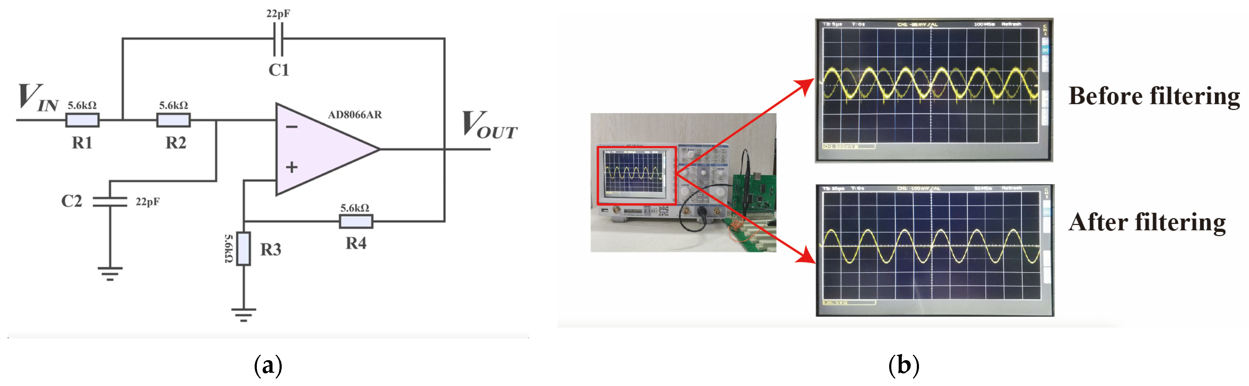
2.2. Improvement of SNR

The flow object composition in the dredging pipe is complex, and due to interference from other electromagnetic components, many electromagnetic signals are carried in the measurement field, which leads to a large amount of high-frequency and low-frequency noise in the measurement circuit. Therefore, it is necessary to conduct spectral analysis in the measurement circuit to observe the frequency distribution of the noise and add corresponding filters to eliminate related noise. At the same time, selecting appropriate electrode materials and transmission signal lines can also reduce external interference to a certain extent. Our study will propose two methods to improve the SNR of EIT.
(1)
Optimization of the measurement circuit
After the excitation signal is added to the sensor, the obtained current signal is transmitted to the FPGA for demodulation through the measurement circuit. The measurement signal carries relevant information about the field conductivity distribution. Due to the complexity of signals in the field of dredging pipes, measurement signals may carry various noise frequencies. Therefore, a series of signal processing circuits must be added to the measurement circuit to obtain high-precision measurement signals.
AD8129 is selected as the cross-resistance amplifier. The signal amplified by AD8129 in the measurement circuit can be observed through an oscilloscope. It is seen that this signal contains higher-order harmonics much higher than 80 kHz. After discrete Fourier transform (DFT) verification, it was observed that this higher-order harmonic signal is approximately in the frequency band of 4 MHz. The structure of the measurement circuit and the DFT results are shown in Figure 2. Where IX is the current to be measured, RO is the resistance value of the sensing resistor, and UO is the partial voltage of the sensing resistor. Therefore, we chose a second-order Salley–Kelly low-pass filter and set its cutoff frequency to 3 MHz. The structure and filtering effect are shown in Figure 3, and it can be seen that most of the noise signals in the measurement signal have been filtered out at this time.
(2)
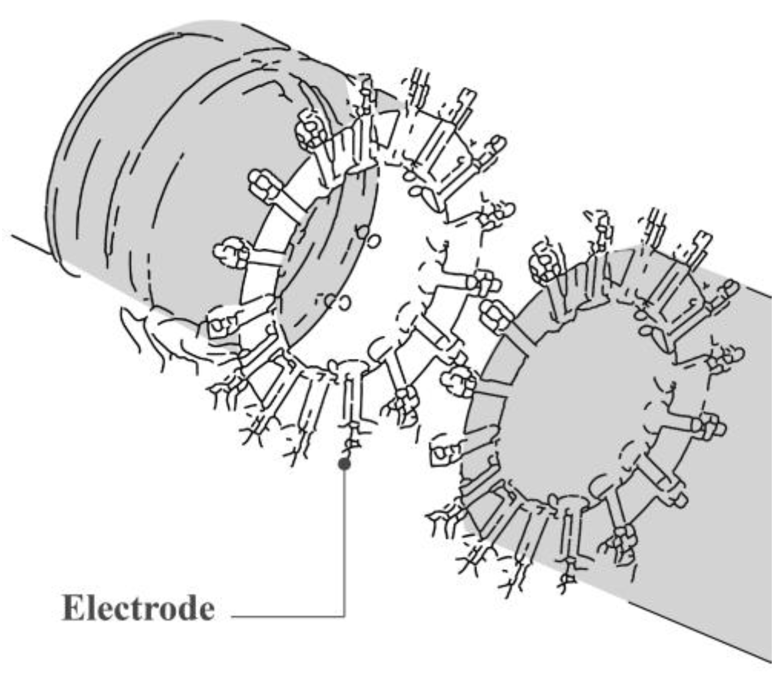
Electrode and transmission line
The sensor electrodes are composed of metal materials arranged at equal intervals inside the pipe or container. They are used to release and obtain electrical signals and are key media for establishing sensitive fields in the measured field domain. These electrode arrays directly affect the potential and equipotential lines of the detection field and have a significant impact on the reconstruction of the conductivity distribution in the measured field [15]. Therefore, sensors used in dredging engineering have high requirements for the materials and manufacturing processes of electrodes and pipes. The internal schematic diagram is shown in Figure 4.
The electrode material must have good conductivity and stable chemical properties. Under the excitation of sinusoidal electrical signals, if the excitation frequency is too low, the polarization reaction on the electrode surface is severe; if the excitation frequency is too high, electromagnetic induction and “connection impedance” will create strong noise [16,17,18,19]. The sensor array of the EIT system is directly in contact with the medium inside the pipe. When an electrical signal is added to any electrode, the electrode will undergo a certain chemical reaction with the substances, thereby affecting the size of the measured value. In the dredging industry, solid materials must be transported through pipes a few kilometers away for reclamation. To cope with the high pressure inside the pipe, electrode materials need to have a certain compressive strength higher than 2.6 MPa. The commonly used materials for electrodes are shown in Table 2.
After comparing the electrode material characteristics mentioned above, titanium was ultimately used as the electrode material instead of traditional stainless steel. Due to the relatively low electrical resistivity and high yield strength of titanium metal, it has good electrochemical stability while meeting lower prices.
In practice, the transmission signal line between the pipe and the data acquisition system is also highly affected by electromagnetic signals generated by other equipment, and these interference sources will directly affect the accuracy of the data collected by the equipment. Therefore, the signal line needs to use a single-core shielded wire with a shielding layer, which can prevent external interference sources from affecting the excitation and measurement signals and also block the path of the signal line, radiating electromagnetic waves outward. The composition of the shielding wire is shown in Figure 5.

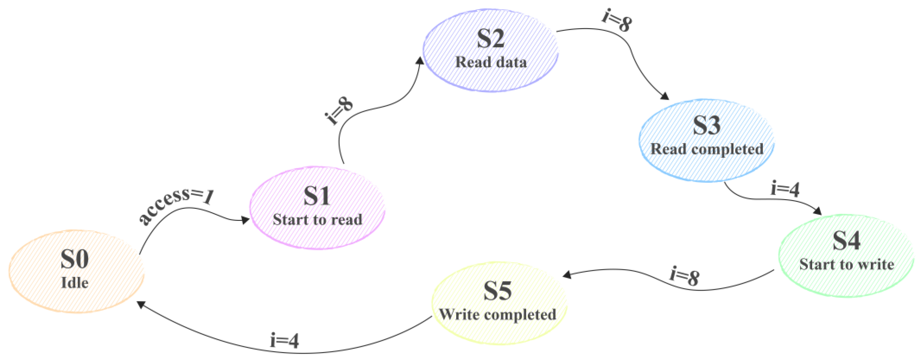
2.3. Improvement of Acquisition Rate

The signal acquisition rate of a data acquisition system is mainly determined by the single cycle time of the system, i.e., the time to obtain a set of measured values. The main factors affecting the single cycle time of the system include the signal frequency released by the FPGA and the transmission rate of the communication module.
(1)
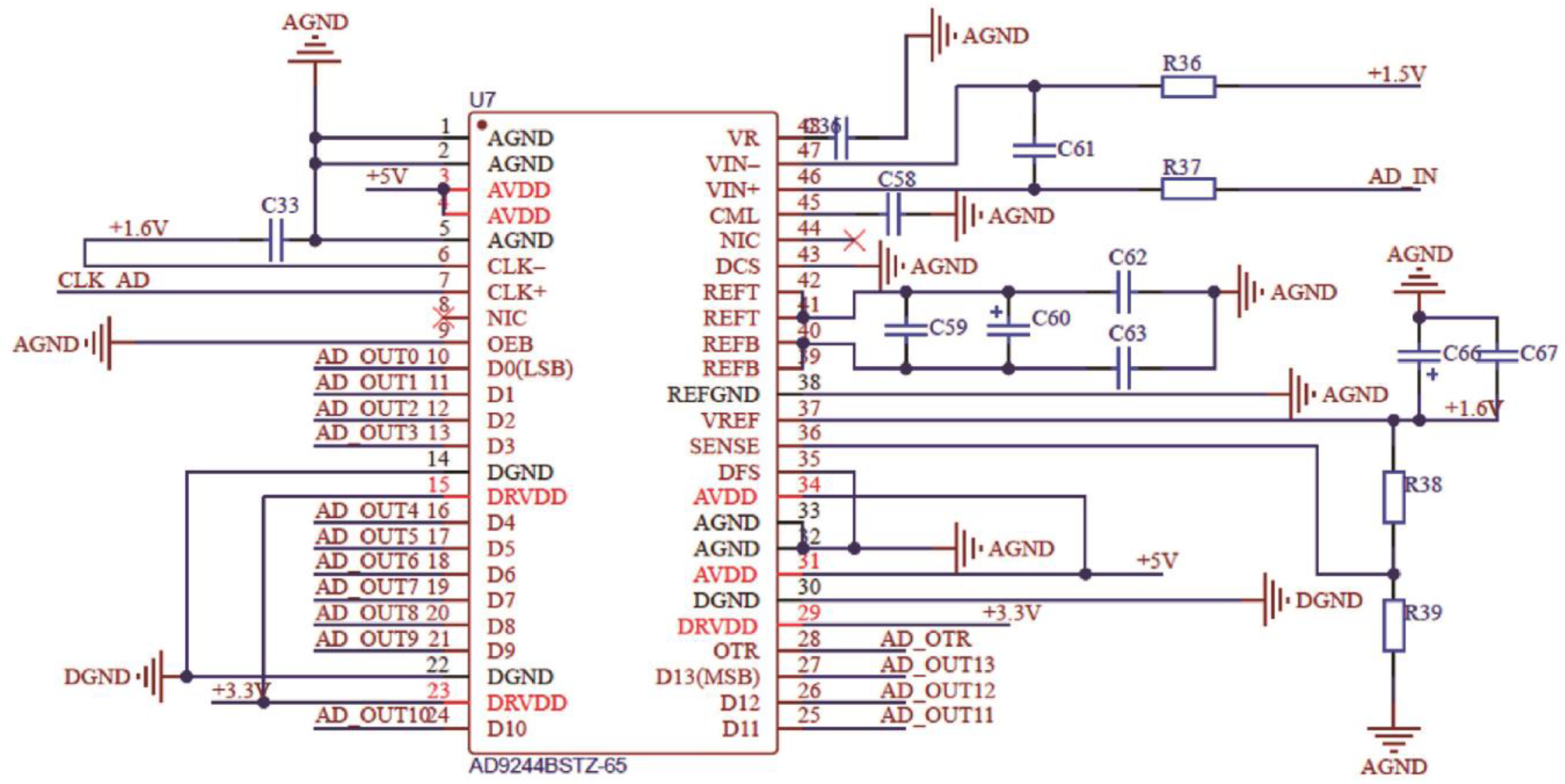
Analog-to-digital conversion optimization
Phase-sensitive demodulation is the most crucial step in obtaining measured values in FPGA. This step requires that the sampling frequency of the A/D module and the D/A module should be consistent. The number of single-cycle semaphores output by analog-to-digital conversion is determined by the sampling frequency of the analog-to-digital conversion chip and the frequency of the analog signal.
n = f s / f
where f is the frequency of the analog signal, fs is the sampling frequency, and n is the number of single-cycle semaphores. The number of different single-cycle semaphores directly determines the final effect of digital-to-analog conversion. The more single-cycle semaphores, the higher the similarity between the output digital signal and the analog signal.
The system has a high demand for signal frequency. The sampling frequency of the A/D and D/A modules must be increased to obtain a higher signal frequency and ensure the current number of single-cycle semaphores. The current sampling frequency of the system is 10 MHz, which is directly provided by FPGA. The highest sampling frequency of the D/A chip AD9764 is 125 MHz, and the highest sampling frequency of the A/D chip AD9240 is 10 MHz.
The current sampling frequency is the highest sampling frequency of AD9240, so the AD9240 chip directly limits the signal frequency of the data acquisition system. Based on the above analysis, it is necessary to replace the A/D conversion chip to improve the signal frequency of the data acquisition system. The common parameters of low-voltage analog-to-digital conversion chips are shown in Table 3.
Considering sampling frequency, cost, accuracy, and other conditions, a 14-bit high-speed analog-to-digital converter AD9244 was ultimately adopted. Its peripheral circuit design is shown in Figure 6.
(2)
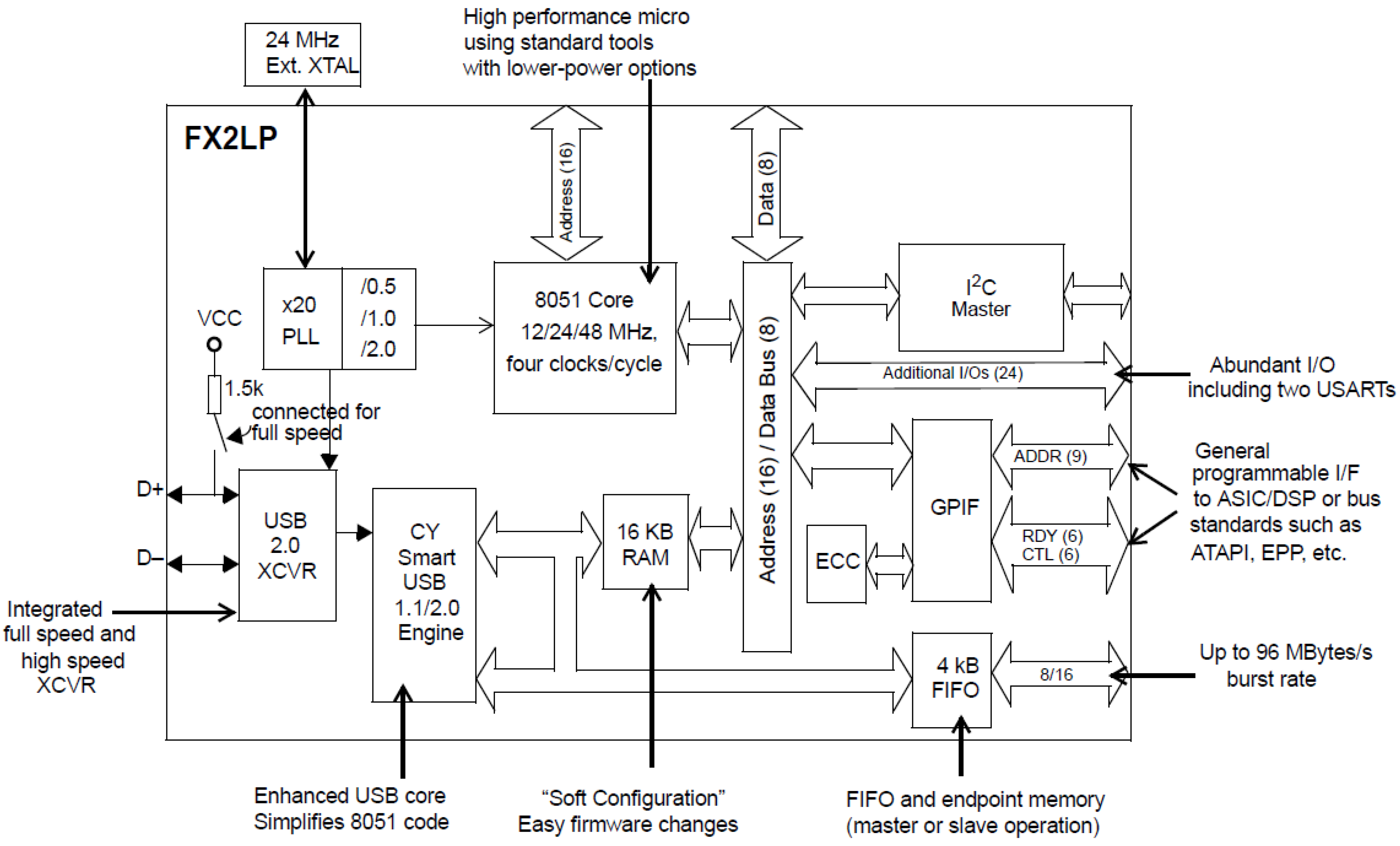
Communication protocol optimization
As one of the key components of the data collection system, the reliability, stability, and real-time performance of the data transmission system will directly affect the performance of the entire system [20]. For an electrical imaging system with n0 electrodes in a single cross-section, the voltage value between each two electrodes is measured after the sensitive field is established, and then the image is reconstructed. The number of measurements required to reconstruct an image is
n 1 = n 0 ( n 0 1 )
Because each measurement data contains 16 bits of real and imaginary data, the number of bytes required to reconstruct an image is
n 2 = 2 n 1
Therefore, for the existing 16-electrode system, the data required to reconstruct an image is 480 B. In addition, each frame of data will also include a frame header and a frame footer, resulting in a data volume of 504 B per frame.
Currently, the data transmission methods commonly used in EIT data collection systems both domestically and internationally include USB, RS-232/485, Ethernet, Firewire, Peripheral Component Interconnect (PCI) interface, etc. [21,22,23]. The maximum transmission rates and characteristics of the various transmission methods mentioned above are shown in Table 4.
The existing EIT system uses RS-232 serial port transmission and can only support transmission rates up to tens of frames per second. This results in the system’s data collection rate being limited by the data transmission method. The existing serial communication can no longer meet the system’s requirements for real-time and reliability. A transmission rate of over 1000 frames per second can meet the real-time requirements of the system [24]. Since the amount of data per frame is 504 B, the transmission rate of the data transmission interface should be greater than 504 kB/s, which is 4.032 Mbps when converted to Baud. Except for RS-232/485, all other transmission methods in Table 4 can meet the transmission speed requirements. Due to the low development cost and good universality of USB2.0, USB2.0 was chosen for the EIT data collection system.
We adopted the CY7C68013A chip from Cypress’s EZ-USB FX2LP series. CY7C68013A is a USB2.0 control chip from Cypress, which includes a high-speed USB2.0 communication protocol and compatible 8051 control. This chip contains 16 KB of internal RAM, allowing firmware programs to run directly without the need for additional memory. CY7C68013A integrates four first-in, first-out (FIFO) internally, with a total size of 4 K bytes. Users can set them to work in master or slave mode. CY7C68013A contains an I2C interface for connecting to external EEPROMs. Users first download the written firmware program to the EEPROM. When CY7C68013A is powered on and started, it will automatically read the EEPROM program and start running in the internal RAM. The internal structure of CY7C68013A is shown in Figure 7.
The data communication between FPGA and USB chips is achieved by reading and writing FIFO data from the four ports (EP2, EP4, EP6, EP8) of CY7C68013A. The FPGA is the main device, and the port of CY7C68013A is the slave device. The slave FIFO can operate in synchronous or asynchronous mode. Due to the internal clock of the chip being 48 MHz and the clock of the EIT system being 50 MHz, the slave FIFO is set to operate in asynchronous mode.
The firmware program of CY7C68013A was completed in the Keil uVision development environment. Through the firmware program, configure the dual function IO of CY7C68013A to Slave FIFO mode, pin FLAGA to indicate the empty flag of EP2 port, FLAGB to indicate the full flag of EP2 port, and FLAGC to indicate the full flag of EP6 port. Additionally, ports 2 and 4 are configured as Bulk outputs, while ports 6 and 8 are configured as Bulk inputs. Burn the generated iic file into the chip’s EEPROM to ensure that the power on the program is not lost.
The reading and writing timing diagram of the chip is shown in Figure 8. The read-and-write control of the chip is implemented by two state machines, and its program is written in Verilog. The state transition diagram of the reading and writing process is shown in Figure 9.

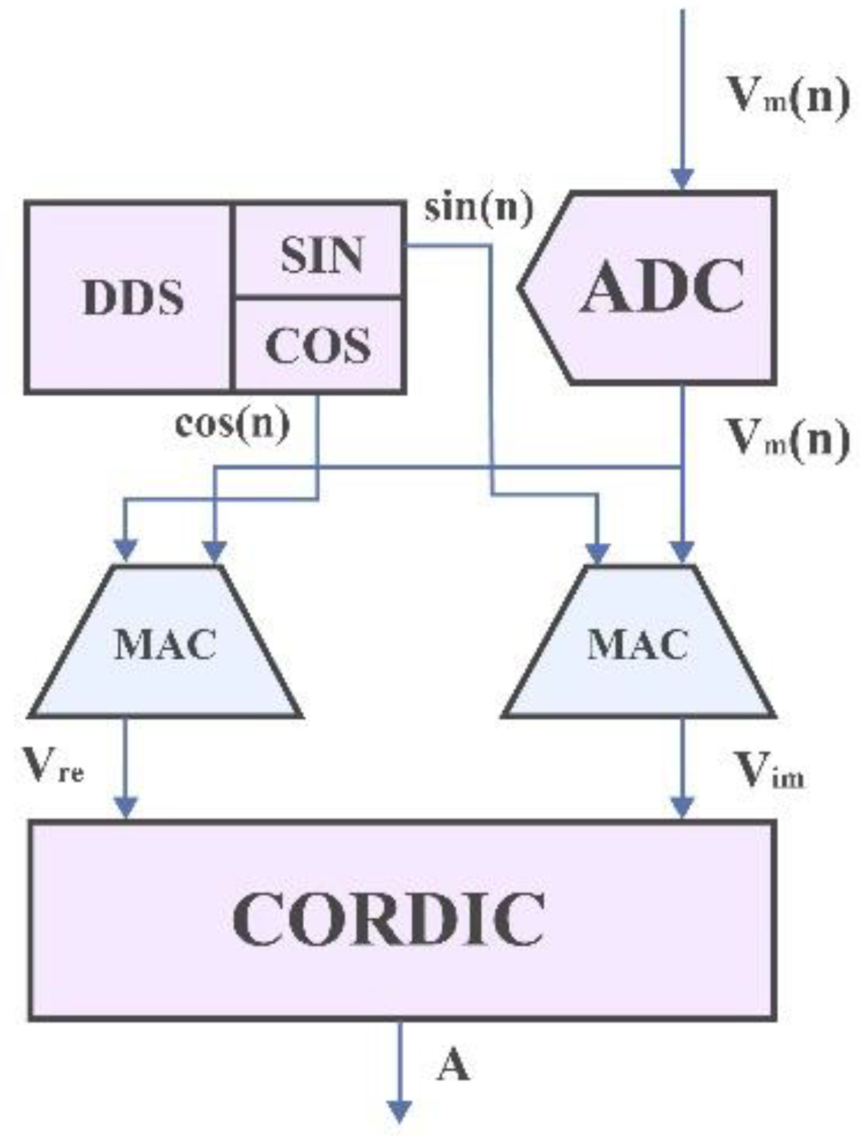
2.4. Digital Phase-Sensitive Demodulation Technique
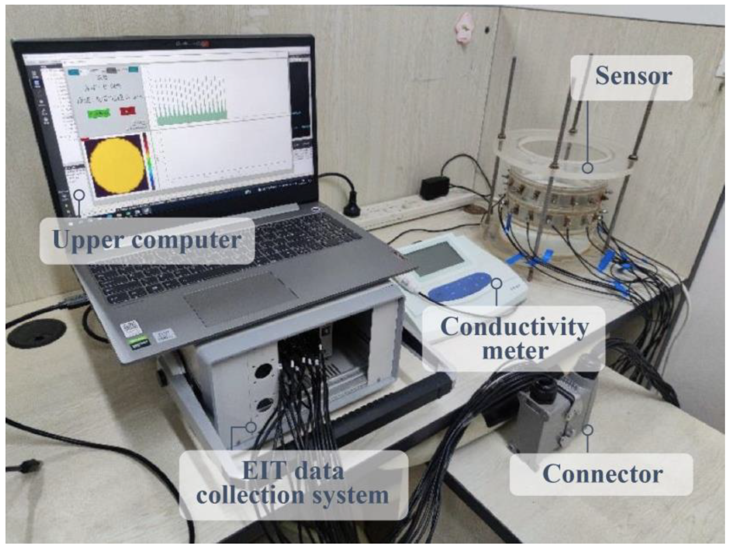
Without considering environmental interference and noise effects, the sine excitation signal output by the data acquisition system may change in amplitude and phase when passing through the measured field domain, while the frequency and waveform remain unchanged. Therefore, the basic form of the discrete signal of Vm(i) that represents the magnitude of voltage received by FPGA can be expressed as
V m ( i ) = A sin ( 2 π i / N + θ )
where A is the amplitude of the sine wave, and N represents the number of sampling points of the AD converter within one excitation signal cycle. Obviously, such a digital signal sequence requires processing to obtain the sine wave amplitude required for image reconstruction. Taking the maximum value point Vmax in a cycle as the value of A is a simple and effective method. However, this method will result in extremely low noise immunity, and any noise that causes a change in the maximum value will have a significant impact on the results. Another method is to directly transmit the amplitude of these discrete signals to the upper computer, which utilizes its powerful data processing function for calculation. However, this requires transmitting N data per cycle, which is very detrimental to the real-time performance of the system.
To address the above issues, digital phase-sensitive demodulation technology is adopted, which converts the discrete signal into a sine wave amplitude through multiplication accumulation and coordinate conversion in FPGA and then transmits it to the upper computer. This method has good anti-interference performance. Due to the parallel execution of instructions in FPGA and the need to transmit only one data to the upper computer, it has almost no impact on the real-time performance of the system.
In Equation (4), Vm represents the voltage to be measured. Assuming Vre represents the real part of Vm and Vim represents the imaginary part of Vm, they can be represented as
V r e = 2 N i = 0 N 1 V m ( i ) × sin 2 π i N = A cos θ
V i m = 2 N i = 0 N 1 V m ( i ) × cos 2 π i N = A sin θ
Therefore, the amplitude of Vm(i) can be expressed as
A = V r e 2 + V i m 2
According to the above formula, digital phase-sensitive demodulation is achieved using the Multiply Accumulate (MAC) and Coordinate Rotation Digital Computer (CORDIC) modules in FPGA. The designed module block diagram is shown in Figure 10.
Vm (n) represents the discrete voltage value to be measured after AD conversion. Two MACs are used to perform cross-correlation operations with the reference signals sin(n) and cos(n), respectively, to obtain the real and imaginary values. Take the output of MAC as the input of CORDIC and perform modulus calculation to obtain the amplitude of the signal to be tested. Using digital phase-sensitive demodulation technology effectively ensures the real-time performance of the system and improves the data acquisition speed.

3. Results

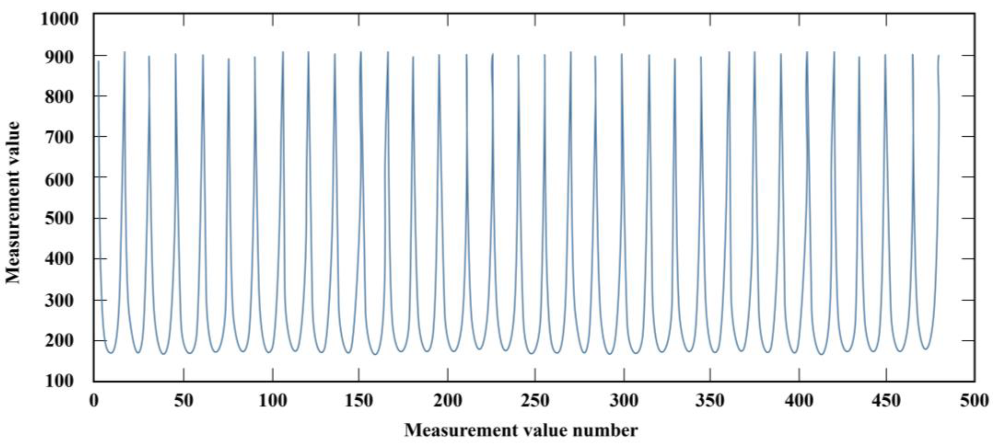
3.1. Experiment on Static Objects

To test the optimization effect of the proposed scheme on the EIT acquisition system, static experiments were conducted to test the SNR of the current system using the optimized EIT acquisition system. The output waveform frequency of the FPGA DDS IP core is set to 160 kHz, and the sampling frequency of AD9764 and AD9244 is set to 20 Mhz. At this time, the excitation frequency of the entire system is 160 kHz. The inner diameter of the static water basin device is 16 cm, and the liquid phase background is tapping water with a conductivity of 260 μS/cm. The entire testing device is shown in Figure 11.
Set the excitation size to 2 V and continuously collect 1000 sets of measurement values in the pure water. After performing SNR analysis on the current system using continuous multiple sets of measurement data, the calculation formula for SNR is as follows:
S N R = 20 lg ( σ x / x ¯ )
where σx represents the standard deviation of the measured values and x ¯ represents the average of the measured values.
The measurement value sequence consists of 480 measurements, and they are shown in Figure 12. To measure the anti-interference ability of the entire EIT system, it is necessary to calculate the SNR of the EIT acquisition system for 480 measurements separately and then calculate the expected values of all results to obtain the SNR of the entire system. The SNR of some measured values is shown in Table 5.
From Table 5, it can be seen that the SNR of most measured values is above 65 dB, and some measured values have no fluctuations in 1000 sets of data, with a standard deviation of 0, indicating a good SNR. When calculating the expected SNR of all measured values, the parameter with an SNR of “/” is set to 100 dB, resulting in an SNR of 73 dB for the current system. Compared to other EIT systems, both domestically and internationally, it can reach a higher level [25,26]. The EIT system in the article is optimized based on our previous work. The original EIT system has an SNR of 52 dB. The comparison results show that the optimized EIT measurement system has significantly improved SNR.

3.2. Simulation Results

Simulate the reading and writing process of the communication module using Modelsim simulation software, and the simulation results are shown in Figure 13. Among them, USB_ ADDR is an addressing signal for FIFO. When the values of this signal are 00 and 10, the communication module performs read and write functions, respectively. The results of the simulation experiment indicate the feasibility of the USB2.0 communication used in this simulation.
After compiling the Verilog program and burning it into FPGA, the EZ-USB Interface was used as a communication tool for data communication. The results showed that USB2.0 communication based on CY68013A could be successfully applied to existing EIT devices.
The communication speed of the communication module is the most concerning issue. To test the actual communication speed of the communication module in this study, the upper computer program Streamer provided by Cypress company was used to test the USB transmission speed. After connecting the main control circuit board of the system to the computer using a USB transmission cable, open the Streamer to establish the connection. After selecting the corresponding read and write ports, the operator can initiate data transmission and monitor the transmission speed in real-time through the Streamer. The test results are shown in Figure 14, with a transmission rate of 40,500 KB/s, which is 316.4 Mbps; The receiving rate is 45,000 KB/s, 351.6 Mbps. Based on the calculation of the frame rate in Section 2, it can be seen that the optimized communication method can allow data transmission over 10,000 frames per second, greatly improving the system’s data acquisition rate.

4. Conclusions

To improve the performance of the data acquisition system used in dredging engineering, in this study, we propose an optimization scheme. To enhance the anti-interference and real-time performances, the sensor array, data acquisition system, and data communication module in the system are optimized to improve the SNR and data acquisition rate. Experimental results show that the optimized system has an SNR of 73 dB and a data transmission rate of 316.4 Mbps, which outperforms the existing system. Therefore, the proposed optimization scheme can extend the EIT applicable range owing to the improvement of the measuring quality.
Further work is focused on integrating multiple excitation modes into a system to cope with complex measuring conditions.

Author Contributions

Conceptualization, N.L. and S.Y.; methodology, N.L. and S.Y.; software, N.L. and Y.W.; validation, N.L., S.Y. and Y.W.; writing—original draft preparation, N.L. All authors have read and agreed to the published version of the manuscript.

Funding

This research was funded by the National Natural Science Foundation of China under Grant No. 61973232.

Institutional Review Board Statement

Not applicable.

Informed Consent Statement

Not applicable.

Data Availability Statement

The data presented in this study are available on request from the corresponding author. The data are not publicly available due to privacy.

Acknowledgments

We would like to acknowledge Engineer Chen from Tianjin Dredging Co., Ltd. for his technical and equipment support.

Conflicts of Interest

The authors declare no conflict of interest.

References

  1. Khang, H.S.; Lee, B.I.; Oh, S.H.; Woo, E.J.; Lee, S.Y.; Cho, M.H.; Kwon, O.; Yoon, J.R.; Seo, J.K. J-substitution algorithm in magnetic resonance electrical impedance tomography (MREIT): Phantom experiments for static resistivity images. IEEE Trans. Med. Imaging 2002, 21, 695–702. [Google Scholar] [CrossRef] [PubMed]
  2. Tan, C.; Lv, S.; Dong, F.; Takei, M. Image Reconstruction Based on Convolutional Neural Network for Electrical Resistance Tomography. IEEE Sens. J. 2019, 19, 196–204. [Google Scholar] [CrossRef]
  3. Brown, B.H.; Seagar, A.D. The Sheffield data collection system. Clin. Phys. Physiol. Meas. 1987, 8, 91. [Google Scholar] [CrossRef] [PubMed]
  4. Smith, R.W.; Freeston, I.L.; Brown, B.H. A real-time electrical impedance tomography system for clinical use-design and preliminary results. IEEE Trans. Biomed. Eng. 1995, 42, 133–140. [Google Scholar] [CrossRef] [PubMed]
  5. Wilson, A.; Milnes, P.; Waterworth, A.; Smallwood, R.H.; Brown, B.H. Mk3.5: A modular, multi-frequency successor to the Mk3a EIS/EIT system. Physiol. Meas. 2001, 22, 49. [Google Scholar] [CrossRef]
  6. Holder, D.; GonzÁlez-Correa, C.; Tidswell, T.; Gibson, A.; Cusick, G.; Bayford, R.H. Assessment and Calibration of a Low-Frequency System for Electrical Impedance Tomography (EIT), Optimized for Use in Imaging Brain Function in Ambulant Human Subjects. Ann. N. Y. Acad. Sci. 1999, 873, 512–519. [Google Scholar] [CrossRef] [PubMed]
  7. Halter, R.; Hartov, A.; Paulsen, K.D. Design and implementation of a high frequency electrical impedance tomography system. Physiol. Meas. 2004, 25, 379. [Google Scholar] [CrossRef]
  8. Sohal, H.; Wi, H.; Mcewan, A.L.; Woo, E.J.; Oh, T.I. Electrical impedance imaging system using FPGAs for flexibility and interoperability. Biomed. Eng. Online 2014, 13, 126. [Google Scholar] [CrossRef]
  9. Cui, Z.Q.; Wang, H.X.; Tang, L.; Zhang, L.; Chen, X.; Yan, Y. A specific data acquisition scheme for electrical tomography. In Proceedings of the 2008 IEEE Instrumentation and Measurement Technology Conference, Victoria, BC, Canada, 12–15 May 2008; pp. 726–729. [Google Scholar]
  10. Hou, H.L.; Wang, H.X.; Chen, X.Y. A biological electrical impedance imaging hardware system based on multi period undersampling technology. Chin. J. Sens. Actuators 2015, 28, 211–216. [Google Scholar]
  11. Wang, Z.Y.; Yue, S.H.; Li, Q.; Liu, X.; Wang, H.; McEwan, A. Unsupervised Evaluation and Optimization for Electrical Impedance Tomography. IEEE Trans. Instrum. Meas. 2021, 70, 1–12. [Google Scholar] [CrossRef]
  12. Zhao, Y.; Wang, P.; Zhang, Z.L.; He, W. Research on swept frequency electrical impedance tomography system. Chin. Med. Equip. J. 2005, 26, 3–5. [Google Scholar]
  13. Wu, J.C.; Yue, S.H.; Ma, H.T. An experimental device for calibration of concentration and velocity of two-phase flow based on electrical impedance measurement system. In Proceedings of the 2021 IEEE International Instrumentation and Measurement Technology Conference (I2MTC), Glasgow, UK, 17–20 May 2021; pp. 1–5. [Google Scholar]
  14. Xin, C.H. Electrical Impedance Tomography Design and Calculation Technology for Fraction Estimation in Dredging Engineering. Master’s Thesis, Tianjin University, Tianjin, China, 2022. [Google Scholar]
  15. Wang, P. Electrical Resistance Tomography (ERT) Technology and Its Application in Two-Phase Flow Detection. Doctoral Dissertation, Xidian University, Xi’an, China, 2012. [Google Scholar]
  16. Kousaka, H.; Ono, K. Numerical Analysis of the Electromagnetic Fields in a Microwave Plasma Source Excited by Azimuthally Symmetric Surface Waves. Jpn. J. Appl. Phys. 2002, 41, 2199. [Google Scholar] [CrossRef]
  17. Mcadams, E.T.; Jossinet, J.; Lackermeier, A.; Risacher, F. Factors affecting electrode-gel-skin interface impedance in electrical impedance tomography. Med. Biol. Eng. Comput. J. Int. Fed. Med. Biol. Eng. 1996, 34, 397–408. [Google Scholar] [CrossRef] [PubMed]
  18. Wang, M.; Dickin, F.J. Electrical resistance tomography of metal walled vessels and pipes. Electron. Lett. 1994, 30, 771–773. [Google Scholar] [CrossRef]
  19. Weinman, J.; Mahler, J. An analysis of electrical properties of metal electrodes. Med. Electron. Biol. Eng. 1964, 2, 299–310. [Google Scholar] [CrossRef]
  20. Xu, Y.B. Research on Communication Method of Electrical Resistance Tomography System Based on USB Technology. Master Dissertation, Tianjin University, Tianjin, China, 2004. [Google Scholar]
  21. Wang, M.; Ma, Y.X.; Holliday, N.; Dai, Y.; Williams, R.A.; Lucas, G. A high-performance EIT system. IEEE Sens. J. 2005, 5, 289–299. [Google Scholar] [CrossRef]
  22. Wang, B.L.; Huang, Z.Y.; Li, H.Q. Development of a new data acquisition system for electrical capacitance tomography. Chin. J. Sci. Instrum. 2001, 22, 424–427. [Google Scholar]
  23. Yang, D.Y.; Xu, C.L.; Zhou, B.; Wang, S.M. A small aperture high pressure capacitance tomography system based on PCI bus. Chin. J. Sci. Instrum. 2007, 28, 1399–1404. [Google Scholar]
  24. Cui, Z.Q.; Wang, H.X. Improvements on real-time performance of electrical capacitance tomography. Chin. J. Sci. Instrum. 2010, 31, 1939–1945. [Google Scholar]
  25. Chen, X.Y.; Sun, L.; Chu, M.L. Research on embedded electrical impedance measurement system. Chin. J. Electron Devices 2017, 40, 430–434. [Google Scholar]
  26. Halter, R.J.; Hartov, A.; Paulsen, K.D. A Broadband High-Frequency Electrical Impedance Tomography System for Breast Imaging. IEEE Trans. Biomed. Eng. 2008, 55, 650–659. [Google Scholar] [CrossRef] [PubMed]
Figure 1. EIT system composition.
Applsci 13 09931 g001
Figure 2. Measurement circuit and DFT result. (a) Measurement circuit; (b) DFT result.
Applsci 13 09931 g002
Figure 3. Filter structure and filtering effect. (a) Filter structure; (b) Filtering effect.
Applsci 13 09931 g003
Figure 4. EIT sensor structure.
Applsci 13 09931 g004
Figure 5. Composition of shielding wire.
Applsci 13 09931 g005
Figure 6. Design of peripheral circuit for AD9244 analog-to-digital conversion module.
Applsci 13 09931 g006
Figure 7. Internal structure diagram of CY7C68013A.
Applsci 13 09931 g007
Figure 8. Reading and writing the timing diagram of the chip. (a) Read; (b) Write.
Applsci 13 09931 g008
Figure 9. Read and write state machine.
Applsci 13 09931 g009
Figure 10. Module diagram of digital-phase sensitive demodulation.
Applsci 13 09931 g010
Figure 11. Experimental device for the test of static objects.
Applsci 13 09931 g011
Figure 12. Measurement value sequence.
Applsci 13 09931 g012
Figure 13. Communication module reading and writing simulation results. (a) Write; (b) Read.
Applsci 13 09931 g013
Figure 14. Data transmission and reception rate monitoring results. (a) Transmission Rate; (b) Receiving rate.
Applsci 13 09931 g014
Table 1. Workflow of the EIT acquisition process.
Step 1: Generate a digital sine wave from FPGA.
Step 2: Drive an external DA conversion chip to generate an AC signal.
Step 3: Load filtered smooth signal to the sensor electrode.
Step 4: Measure the current signal and convert it into a digital signal through an AD conversion chip.
Step 5: Transfer the digital signal to FPGA for demodulation to obtain its amplitude.
Step 6: Process the data collected by the EIT system through the upper computer.
Table 2. Characteristics of electrode materials at room temperature.
MaterialResistivity (Ω∙m)Yield Strength (MPa)Electrochemical CharacteristicsPrice (RMB/ton)
Copper1.72 × 10−8343Strong stability and corrosion resistance62,980
Titanium4.2 × 10−7300Good stability and corrosion resistance62,210
Carbon3.5 × 10−69.3Non-metallic, corrosion-resistant2000
Tungsten5.48 × 10−8-Strong stability and corrosion resistance116,000
Stainless steel7.3 × 10−7207Moderate stability, not resistant to corrosion15,625
Table 3. Performance parameters of common analog-to-digital conversion chips.
ChipMaximum Sampling Rate (MSPS)Packaging TypeResolution Ratio/Bit Wide (bit)SNR (dB)
AD924010MQFP-441478.5
AD924465LQFP-481475.3
LTC223980QFN-321061.6
ADS4149250VQFN-481472.2
Table 4. Comparison of data transmission methods.
Data Transmission MethodRateDistanceCharacteristic
USB2.0480 Mbps5 mLow-cost, widely used
RS-232/485115,200 bps1200 mSimple but low-speed
Ethernet(IEEE 802.3ab)1 GbpsHundreds of kilometersRelatively complex, capable of remote communication
Firewire(IEEE 1394c-2006)800 Mbps4.5 mLess CPU usage, reliability, and high-cost
PCI(PCI-X 3.0)4266 MB/s-Belongs to the local bus
Table 5. SNR situation of some measured values.
Measurement Data Number x ¯ σxSNR (dB)
608980/
182410.980.040880.0656
2832930/
290197.99500.070568.9652
327236.980.040875.0986
396180.99000.099565.1967
442174.00160.040772.5998
473169.99830.040872.3976
Disclaimer/Publisher’s Note: The statements, opinions and data contained in all publications are solely those of the individual author(s) and contributor(s) and not of MDPI and/or the editor(s). MDPI and/or the editor(s) disclaim responsibility for any injury to people or property resulting from any ideas, methods, instructions or products referred to in the content.

