Brief Report

A Palladium-Deposited Molybdenum Disulfide-Based Hydrogen Sensor at Room Temperature

Department of Electric Engineering, Gangneung-Wonju National University, Gangneung 25457, Republic of Korea
*
Author to whom correspondence should be addressed.
Appl. Sci. 2023, 13(19), 10594; https://doi.org/10.3390/app131910594
Submission received: 29 August 2023 / Revised: 18 September 2023 / Accepted: 20 September 2023 / Published: 22 September 2023

Abstract

:
Recently, hydrogen (H2) energy has attracted attention among eco-friendly energy sources because H2 energy is eco-friendly, energy-efficient, and abundant in nature. However, when the concentration of H2 in the atmosphere is more than 4%, H2 has a risk of explosion. H2 is a colorless, tasteless, and odorless gas that is difficult to detect with human senses. Therefore, developing an optimized hydrogen sensor is essential. Palladium (Pd) has good reactivity to hydrogen. Molybdenum disulfide (MoS2) has high carrier mobility, sensitive reactivity to toxic gases, and high surface-area-to-volume ratio. Therefore, we proposed hydrogen sensors that use Pd and MoS2. The main fabrication processes include MoS2 deposition through CVD and Pd deposition through DC sputtering. In this study, we utilized Pd and MoS2 to enable sensing at room temperature. By optimizing the Pd to a nanoparticle structure with an expansive surface area of 4 nm, we achieved a fast response time of 4–5 s and an enhanced yield through a simplified structure. Hydrogen sensors inherently exhibit sensitivity to various environmental factors. To address these challenges, technologies such as machine learning can be incorporated. Emphasizing low-power consumption and various application compatibilities becomes pivotal to promoting commercialization across diverse industries.

1. Introduction

Recently, global interest in eco-friendly energy sources has increased in response to pressing concerns about climate change and the depletion of fossil fuels. Among new sustainable energy options, H2 energy has received considerable attention. H2 is an eco-friendly, energy-efficient, and richly available energy source and has the potential to be a key competitor in the pursuit of sustainable power generation. However, the remarkable potential of H2 energy is coupled with the inherent challenge of requiring innovative solutions. One of the significant challenges associated with H2 is its unique properties. H2 is a colorless, odorless, and tasteless gas that is seemingly harmless but can be highly flammable and explosive if the concentration in the surrounding air exceeds 4% [1]. This property poses a significant safety risk, especially in industries where H2 is an important component. To reduce the potential risks and protect both people and infrastructure, the timely detection of H2 leaks is essential. For this reason, hydrogen sensors have become an integral part of various industries that rely on H2. Hydrogen sensors play a pivotal role in ensuring safety by accurately detecting H2 leaks early on. For practical applications in a variety of industrial environments, hydrogen sensors must satisfy the criteria of being cost-effective, compact, energy-efficient, and have high-performance results.
The hydrogen sensors available in the market are typically categorized into several types, including electrochemical sensors, catalyst-based sensors, work function-based sensors, and resistive-based sensors. Among them, electrochemical and chemiresistive hydrogen sensors are attracting attention for being commercially available sensors. Electrochemical sensors are sensitive, selective, and have a low limit of detection (LOD); however, they are highly sensitive to ambient conditions and require high manufacturing costs. On the other hand, chemiresistive sensors have advantages, such as efficient sensing performance, low-cost manufacturing, and low power. Among the chemiresistive sensors, Pd-based resistive sensors and semiconducting metal oxide (SMO)-based sensors are being actively studied. Pd-based resistive sensors provide simplicity, high reactivity to H2, and detection at room temperature but reduce the detection performance in ambient air. SMO-based sensors have been commercialized due to their effectiveness and high compatibility with H2 detection. The SMO-based sensor has a high operating temperature. High operating temperatures not only increase power consumption but also increase the combustibility of H2, which creates a risk of explosion [2,3,4].
The recent rapid development of sensor technology has revealed many application methods. In particular, nanowire structures are attracting attention as one of the most promising methods thanks to their excellent reactivity and proficiency in detection. Among these developments, research by Sihang Lu et al. deserves to be noted. Their exploration of the utilization of Pd/SnO2 nanowire structures showed remarkable reactivity to hydrogen. However, an important consideration is the operating requirement of relatively high temperatures, especially at about 150 °C [5]. Therefore, the development of reliable hydrogen sensors that can operate at room temperature is the most important factor.
Previous researchers were interested in two-dimensional (2D) materials, which are now attracting attention in various scientific fields due to their unique structural, electronic, and mechanical properties. Graphene, in particular, is a subject of extensive research due to graphene’s excellent properties within the domain of 2D materials. However, the application of graphene as a sensor is limited in certain situations due to the difficulty in controlling its band gap [6]. For this reason, MoS2 has received a lot of attention because its bandgap is adjustable. MoS2 is connected by a relatively weak van der Waals force. This means that the gas molecules can freely penetrate and diffuse through the layers. MoS2-based sensors are being actively studied in the field of gas detection. An MoS2 -based sensor has excellent potential for gas detection but has low selectivity and a high operating temperature for hydrogen [7]. To overcome these limitations, Pd with good reactivity and selectivity to hydrogen was proposed as a catalyst [8]. We proposed a Pd-deposited MoS2-based hydrogen sensor operating at room temperature.

2. Nanocomposite Materials

Nanocomposites are the focus of extensive research due to their unique properties, including remarkable electrical, optical, chemical, and mechanical characteristics. Nanocomposites have demonstrated applications across a multitude of industries. Among the various 2D materials, MoS2 has drawn particularly significant attention from researchers. MoS2 exhibits exceptional properties, such as high carrier mobility, sensitivity to toxic gases, and a substantial surface-area-to-volume ratio [9,10]. One of the main areas of exploration related to MoS2 is the application of hydrogen sensor development. However, conventional MoS2-based hydrogen sensors have posed challenges due to their high operating temperatures. In response to this limitation, noble metals have emerged as valuable catalytic materials. Among the catalysts, Pd can effectively dissociate H2 gas and then adsorb H2 atoms onto the surface. Pd-induced catalysis significantly reduces the activation energy required for the chemical reactions associated with hydrogen detection. Consequently, Pd not only enhances the response time but also enables operation at lower temperatures, thus improving the overall efficiency and reliability of hydrogen sensors [11].

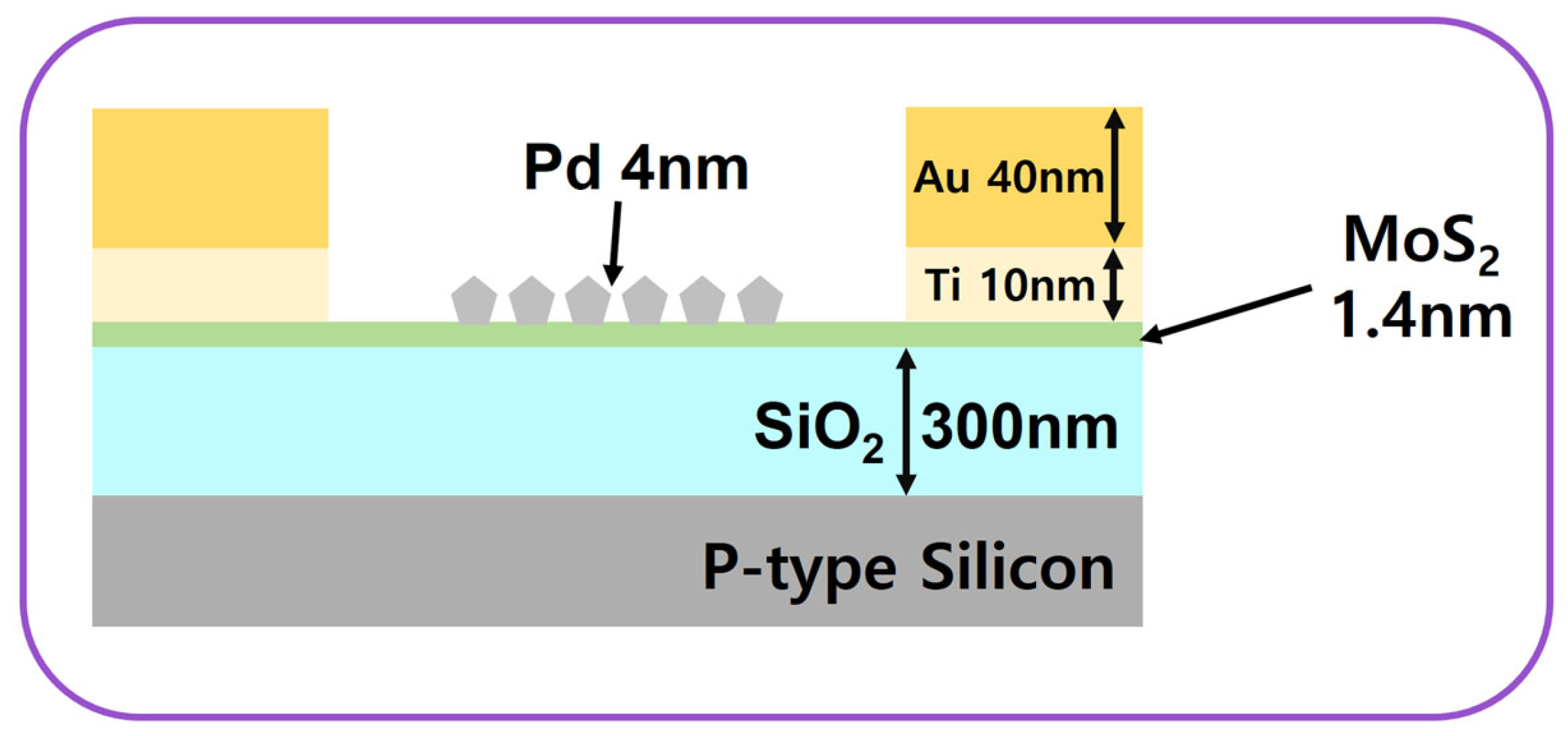
3. Fabrication Process

Figure 1 illustrates the comprehensive fabrication process employed in creating the Pd-deposited MoS2-based hydrogen sensor. The process initiates with the preparation of a Si wafer, onto which a layer of silicon dioxide is meticulously deposited, reaching a thickness of 300 nm via the wet oxidation technique. Subsequently, the crucial channel material, MoS2, is deposited utilizing chemical vapor deposition (CVD) methodology. In the CVD process, the MoS2 deposition takes place under specific conditions: the central heating zone maintains a temperature of 720 °C, while the upstream zone maintains a temperature of 200 °C. Furthermore, Ar gas is introduced at a rate of 200 standard cubic centimeters per minute (SCCM), effectively maintaining ambient pressure within the system.
To facilitate this deposition, a combination of molybdenum trioxide powder (2 mg) and sulfur powder (100 mg) is placed in quartz tubes inserted into larger quartz tubes within a three-zone tube furnace. Throughout this process, MoS2 accumulates to a thickness of approximately 1.4 nm, constituting approximately eight layers. Following the deposition phase, a patterning step is introduced through a lithography process. Within this process, an initial cleaning procedure is conducted, involving successive treatments with acetone, an isopropyl alcohol (IPA) solution, deionized water (DI-water), and N2 gas. Subsequently, a positive photoresist (PR) is applied, forming a PR coating at an RPM of 5000 for 40 s. The coated substrate is then subjected to a hot plate at 100 °C for 1 min to eliminate the solvent. A mask is then strategically placed over the sample, which is subsequently exposed to ultraviolet (UV) light. Finally, the photoresist is removed utilizing a developer solution. In the final phase of the fabrication process, Pd is deposited onto the MoS2 layer through DC sputtering. The deposition parameters are precisely controlled, with Pd being deposited for 4 s, employing an Ar flow rate of 30 sccm and a power of 100 W. The resulting Pd layer exists in the form of discrete Pd particles, characterized by a thickness of 4 nm. To conclude the process, electrodes are introduced, comprising a Ti layer with a thickness of 10 nm, followed by a Au layer with a thickness of 40 nm, both deposited through DC sputtering.
Figure 2 presents a schematic representation of the Pd-deposited MoS2-based hydrogen sensor, offering insights into its structure and key features. The thickness of the Pd layer plays a critical role in determining sensor performance. When the Pd layer is extremely thin, such as 1 nm, the Pd particles become indistinct, resulting in a limited contact area with the MoS2 layer. As a result, sensitivity is compromised, and the response time is relatively slow. Conversely, as the thickness of the Pd layer increases, the increased contact area of the Pd improves both the sensitivity and reactivity. However, deposition of the Pd into a continuous layer can lead to a decrease in sensitivity and response time. This reduction is attributed to a reduced contact area and the accumulation of an electric charge. Therefore, a balance must be struck to optimize sensor performance. To achieve the best sensing properties, the researchers in this study decided to deposit Pd particles with a thickness of 4 nm. This thickness represents an optimal compromise and was carefully selected, providing a substantial contact area while preventing the adverse effects associated with thicker Pd layers [12].

4. Results

This section discusses the experimental gas reactions, the operating principles of Pd-deposited MoS2-based hydrogen sensors, and the various measurement results.

4.1. Gas Measurement Method

This section provides a detailed description of the gas measurement technique, encompassing the test conditions, setup protocols, and gas introduction methods.
The gas sensing measurements were conducted within a controlled environment, specifically a gas probe station chamber. During these measurements, the sensor was subjected to a DC voltage of 3.5 V. The H2 concentration was precisely controlled using a mass flow controller (MFC), ensuring accurate and repeatable test conditions. To minimize the influence of other gases and maintain current stability, the sensor was first exposed to N2 gas at a flow rate of 100 SCCM for 1 min. Subsequently, H2 gas was introduced at a flow rate of 20 SCCM, allowing for the measurement of changes in current as a result of H2 presence.

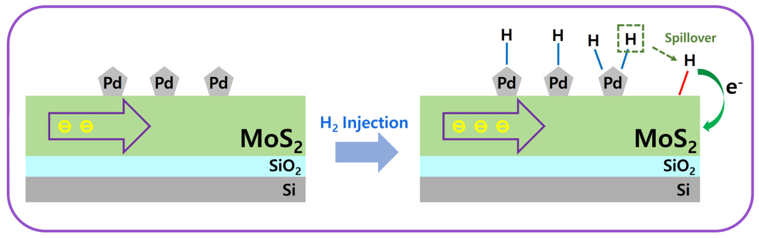
4.2. Gas Sensor Mechanism

This section describes the basic behavior of the MoS2-based hydrogen sensor. Here, we explain the scientific principles of how sensors detect the presence of H2.
The operational framework of the Pd-deposited MoS2-based hydrogen sensor arises from the multifaceted functions of MoS2 within the system. Specifically, MoS2 assumes two critical roles that synergistically contribute to the sensor’s functionality. Firstly, MoS2 serves as the channel through which the current flows. Simultaneously, MoS2 undertakes the task of adsorbing oxygen molecules onto its surface, thereby generating oxygen ion species. This process induces an increase in the resistance of MoS2. This resistance increase can be attributed to the transformation of the adsorbed oxygen into oxygen ion species, involving the exchange of electrons with MoS2 atoms.
Figure 3 shows the mechanism of the Pd-deposited MoS2-based hydrogen sensor. In the absence of injected H2, MoS2 tends to adsorb oxygen on the MoS2 surface, leading to the generation of oxygen ion species. Following the injection of H2, Pd plays a pivotal role. Pd dissociates the H2 molecules, subsequently absorbing the liberated H. A notable phenomenon referred to as the “spillover effect” ensues, wherein hydrogen diffuses from the Pd layer into the MoS2 material. In this dynamic, hydrogen and oxygen ion species combine on the surface of MoS2, culminating in the production of H2O and free electrons. These generated electrons are then introduced into the MoS2 channel, inducing a change in the current flow. Consequently, the Schottky barrier, which governs the flow of electrical charge at the metal–semiconductor interface and experiences alteration, ultimately manifesting as a measurable current change. As such, the hydrogen sensor detects the presence of H2 leakage through the observed variation in current.

4.3. Measurement Result

In the Measurement Result section, we present the spectrum results, analyzing the structural characteristics of MoS2, and the sensor responses at varying H2 concentrations. Additionally, a table is incorporated for comparison with other studies.
The structural properties of MoS2 are precisely analyzed through Raman and photoluminescence (PL) spectroscopy, providing important insights into the properties of materials. Figure 4a shows the Raman spectrum, an important indicator for analyzing the structural properties of MoS2. Two major peaks are important in the Raman spectrum. The first peak, indicated by E1 2g, is related to the crystal structure in the form of MoS2. The position and intensity of the E1 2g peak are greatly influenced by both the crystal structure and the thickness of MoS2. The second peak, designated as A1g, is related to interatomic vibration in the material. A1g is also influenced by crystal structure and thickness, and A1g is an indicator of material quality. In the Raman spectrum, the E1 2g and A1g peaks of the MoS2 monolayer were observed at 382 cm−1 and 402 cm−1, respectively, and the E1 2g and A1g peaks of the multilayer MoS2 were observed at 380 cm−1 and 407 cm−1, respectively. The E1 2g peak corresponds to the in-plane vibration mode, which is the vibration of Mo atoms and S atoms parallel to the layer, and the A1g peak corresponds to the out-of-plane vibration mode, which is the vibration of S atoms perpendicular to the layer. The distance between the two peaks represents the number of layers present in the MoS2 crystal, and as the number of layers increases, the distance between the two peaks increases due to interlayer vibration.
Figure 4b is a PL spectrum graph of MoS2 obtained at a laser wavelength of 532 nm. The PL spectrum of MoS2 provides essential information on electronic states and structural properties. In the PL spectrum, the peak position reflects the bandgap of MoS2. The peak of the monolayer MoS2 is located at 660 nm. The peak of the multilayer MoS2 is located at 995 nm. Applying the conversion relationship between photon energy and laser wavelength, the bandgap of the monolayer MoS2 is calculated as 1.87 eV, and the bandgap of the multilayer MoS2 is calculated as 1.24 eV. This corresponds to a generally known bandgap range of MoS2. The intensity of the PL peak represents the efficiency of the light-emitting process occurring in MoS2 [13].
Figure 5 shows the sensitivity of the Pd-deposited MoS2-based hydrogen sensor according to the H2 concentration at room temperature. Figure 5a shows a H2 concentration of 1% and an average sensitivity of 1.34. Increasing the H2 concentration to 3% in Figure 5b increases the average sensitivity to 2.17, and, finally, the results for the 4% H2 concentration in Figure 5c show the average sensitivity to be 2.77. The response time was 4 to 5 s. Response time is defined as the time when the sensor’s total current changes by 90%. Sensitivity is defined as S = Ig/I0. Ig is the current after injecting the H2 gas, and I0 is the current without H2. The fast response time was caused by the high carrier mobility of MoS2 and the simplification of the process due to the simple structure. Typical MoS2-based sensors have high operating temperatures. However, the sensor showed changes in current to H2 at room temperature. The reason for this is that Pd aggregates hydrogen and promotes the reaction to H2. The sensitivity graph demonstrates that as the sensitivity increases, the H2 concentration increases. The reason for this is the amount of H2 reacting with the Pd particles increases as the concentration of H2 increases. This means that the current increases when increasing the number of electrons injected into the channel.

5. Discussion

In this study, we analyzed the mechanism and performance of Pd-deposited MoS2-based hydrogen sensors. The foundational role of MoS2 in adsorbing oxygen in the absence of H2 and the action of adsorbing hydrogen in the presence of H2 are combined to reveal the characteristics of sensing H2. This “spillover” effect, characterized by H2 dissociation in Pd and the subsequent diffusion to MoS2, highlights the importance of Pd in sensing mechanisms, especially in influencing the Schottky barrier at the metal–semiconductor junction. As shown in Table 1, faster responses at room temperature are prominent compared to previous studies. The fast response time shown by the Pd-deposited MoS2-based hydrogen sensor was caused by various characteristics. The first one contributed to the fast response time by enabling fast current change due to the high electron mobility of MoS2. Both Raman spectroscopy and PL spectroscopy provided a perspective on the structural dynamics of MoS2 for optimization through thickness adjustment. Second, the property of Pd, which quickly adsorbs and dissociates H2 molecules, contributes to a faster reaction time, and Pd thickness optimization ensures the nanoparticle structure of Pd and the wide surface area for efficient H2 adsorption and reaction. In addition, the change in the Schottky barrier due to the interaction of Pd and MoS2 accelerates the electron flow, thereby facilitating the reaction. The optimized thickness of the MoS2 layer can speed up the movement of electrons and improve the response time. Adjusting the Schottky barrier may affect the sensitivity of the sensor.

6. Conclusions

In conclusion, a high-performance hydrogen sensor was presented by optimizing the thickness and structure of Pd and MoS2. Therefore, the excellent response time of 4 to 5 s at room temperature and the simple design resulted in a high yield. Hydrogen sensors are sensitive to environmental factors. With this in mind, it should be considered that future machine learning or similar technologies could be integrated to produce optimized sensors. This would require a low power base and good compatibility of various applications to demonstrate the potential for widespread use in various sectors. Our results, therefore, demonstrate an undeniable possibility. Future research may coordinate MoS2 and Pd deposition technologies and focus on the integration of machine learning technologies.

Author Contributions

Conceptualization, U.J.C.; methodology, B.J., R.K. and Y.K.; validation, D.J. and T.K.; investigation, U.J.C.; re-sources, Y.J.; writing—original draft preparation, U.J.C.; writing—review and editing, U.J.C.; visu-alization, Y.J.; supervision, M.-W.K.; project administration, D.J. and M.-W.K.; funding acquisition, M.-W.K. All authors have read and agreed to the published version of the manuscript.

Funding

We gratefully acknowledge the support from the National R&D Program, facilitated by the National Research Foundation of Korea (NRF). This initiative was generously funded by the Ministry of Science and ICT under grant NRF-2022M3I7A1078936. Further support was extended by the “Regional Innovation Strategy (RIS)” initiative, backed by the Ministry of Education with grant 2022RIS-005. Additionally, our gratitude extends to the Korean government’s MSIT for the assistance provided through the National Research Foundation of Korea grant 2021R1G1A1093786.

Institutional Review Board Statement

Not applicable.

Informed Consent Statement

Not applicable.

Data Availability Statement

No new data were created or analyzed in this study. Data sharing is not applicable to this article.

Conflicts of Interest

The authors declare no conflict of interest.

References

  1. Li, Z.; Yao, Z.; Haidry, A.A.; Plecenik, T.; Xie, L.; Sun, L.; Fatima, Q. Resistive-type hydrogen gas sensor based on TiO2: A review. Int. J. Hydrogen Energy 2018, 43, 21114–21132. [Google Scholar] [CrossRef]
  2. Kuru, C.; Choi, C.; Kargar, A.; Choi, D.; Kim, Y.J.; Liu, C.H.; Yavuz, S.; Jin, S. MoS2 Nanosheet–Pd Nanoparticle Composite for Highly Sensitive Room Temperature Detection of Hydrogen. Adv. Sci. 2015, 2, 1500004. [Google Scholar] [CrossRef] [PubMed]
  3. Rezende, N.P.; Cadore, A.R.; Gadelha, A.C.; Pereira, C.L.; Ornelas, V.; Watanabe, K.; Taniguchi, T.; Ferlauto, A.S.; Malachias, A.; Campos, L.C.; et al. Probing the Electronic Properties of Monolayer MoS2 via Interaction with Molecular Hydrogen. Adv. Electron. Mater. 2019, 5, 1800591. [Google Scholar] [CrossRef]
  4. Koo, W.-T.; Cho, H.-J.; Kim, D.-H.; Kim, Y.H.; Shin, H.; Penner, R.M.; Kim, I.-D. Chemiresistive Hydrogen Sensors: Fundamentals, Recent Advances, and Challenges. ACS Nano 2020, 14, 14284–14322. [Google Scholar] [CrossRef] [PubMed]
  5. Lu, S.; Zhang, Y.; Liu, J.; Li, H.Y.; Hu, Z.; Luo, X.; Gao, N.; Zhang, B.; Jiang, J.; Zhong, A.; et al. Sensitive H2 gas sensors based on SnO2 nanowires. Sens. Actuators B Chem. 2021, 345, 130334. [Google Scholar] [CrossRef]
  6. Zhang, W.; Zhang, P. Synthesis and sensor applications of MoS2-based nanocomposites. Nanoscale 2015, 7, 18364–18378. [Google Scholar] [CrossRef] [PubMed]
  7. Baek, D.-H.; Kim, J. MoS2 gas sensor functionalized by Pd for the detection of hydrogen. Sens. Actuators B Chem. 2017, 250, 686–691. [Google Scholar] [CrossRef]
  8. Jaiswal, J.; Tiwari, P.; Singh, P.; Chandra, R. Fabrication of highly responsive room temperature H2 sensor based on vertically aligned edge-oriented MoS2 nanostructured thin film functionalized by Pd nanoparticles. Sens. Actuators B Chem. 2020, 325, 128800. [Google Scholar] [CrossRef]
  9. Lee, S.; Kang, Y.; Lee, J.; Kim, J.; Shin, J.W.; Sim, S.; Go, D.; Jo, E.; Kye, S.; Kim, J.; et al. Atomic layer deposited Pt nanoparticles on functionalized MoS2 as highly sensitive H2 sensor. Appl. Surf. Sci. 2022, 571, 151256. [Google Scholar] [CrossRef]
  10. Sarkar, D.; Xie, X.; Kang, J.; Zhang, H.; Liu, W.; Navarrete, J.; Moskovits, M.; Banerjee, K. Functionalization of Transition Metal Dichalcogenides with Metallic Nanoparticles: Implications for Doping and Gas-Sensing. Nano Lett. 2015, 15, 2852–2862. [Google Scholar] [CrossRef] [PubMed]
  11. Luo, Y.; Zhang, C.; Zheng, B.; Geng, X. Hydrogen sensors based on noble metal doped metal-oxide semiconductor: A review. Int. J. Hydrogen Energy 2018, 42, 20386–20397. [Google Scholar] [CrossRef]
  12. Hao, L.; Liu, Y.; Du, Y.; Chen, Z.; Han, Z.; Xu, Z.; Zhu, J. Highly Enhanced H2 Sensing Performance of Few-Layer MoS2/SiO2/Si Heterojunctions by Surface Decoration of Pd Nanoparticles. Nanoscale Res. Lett. 2017, 12, 567. [Google Scholar] [CrossRef] [PubMed]
  13. Han, T.; Liu, H.; Wang, S.; Chen, S.; Li, W.; Yang, X.; Cai, M.; Yang, K. Probing the Optical Properties of MoS2 on SiO2/Si and Sapphire Substrates. Nanomaterials 2019, 9, 740. [Google Scholar] [CrossRef] [PubMed]
  14. Luo, Y.; Zhang, C. Pt-activated TiO2-MoS2 nanocomposites for H2 detection at low temperature. J. Alloys Compd. 2018, 747, 550–557. [Google Scholar] [CrossRef]
  15. Vivekanandan, A.K.; Huang, B.-R.; Kathiravan, D.; Saravanan, A.; Prasannan, A.; Tsai, H.-C.; Chen, S.-H. Effect of MoS2 solution on reducing the wall thickness of ZnO nanotubes to enhance their hydrogen gas sensing properties. J. Alloys Compd. 2021, 854, 157102. [Google Scholar] [CrossRef]
Figure 1. The fabrication process of the Pd-deposited MoS2-based hydrogen sensor.
Applsci 13 10594 g001
Figure 2. Schematic of the Pd-deposited MoS2-based hydrogen sensor.
Applsci 13 10594 g002
Figure 3. The mechanism of the Pd−deposited MoS2−based hydrogen sensor.
Applsci 13 10594 g003
Figure 4. (a) Raman spectrum of MoS2; (b) PL spectrum of MoS2 at a 532 nm laser wavelength.
Applsci 13 10594 g004
Figure 5. The sensitivity of the Pd-deposited MoS2-based hydrogen sensor using H2 concentration at room temperature: (a) H2 concentration is 1%; (b) H2 concentration is 3%; (c) H2 concentration is 4%.
Applsci 13 10594 g005
Table 1. Comparison of sensitivity, response time, and conditions for various hydrogen gas sensors.
MaterialsDefinition of SensitivityConcentration
(ppm)
Temperature
(°C)
SensitivityResponse Time (s)Reference
Pd/MoS2(Rg−Ra)/Ra × 100%50,000RT100040[2]
Pt/Tio2/MoS2(Rg-Ra)/Ra20001000.749150[14]
MoS2/ZnORg/Ra × 100%500RT51.514[15]
Pd/MoS2(Rg−Ra)/Ra × 100%500RT33.716[8]
Pd/MoS2(Rg−Ra)/Ra × 100%10,000RT35.3786[7]
Pd/MoS2Ig/I040,000RT2.774~5This work
Disclaimer/Publisher’s Note: The statements, opinions and data contained in all publications are solely those of the individual author(s) and contributor(s) and not of MDPI and/or the editor(s). MDPI and/or the editor(s) disclaim responsibility for any injury to people or property resulting from any ideas, methods, instructions or products referred to in the content.

