
Integrated Hybrid Tweezer for Particle Trapping with Combined Optical and Acoustic Forces

Abstract
:Featured Application
Abstract
1. Introduction
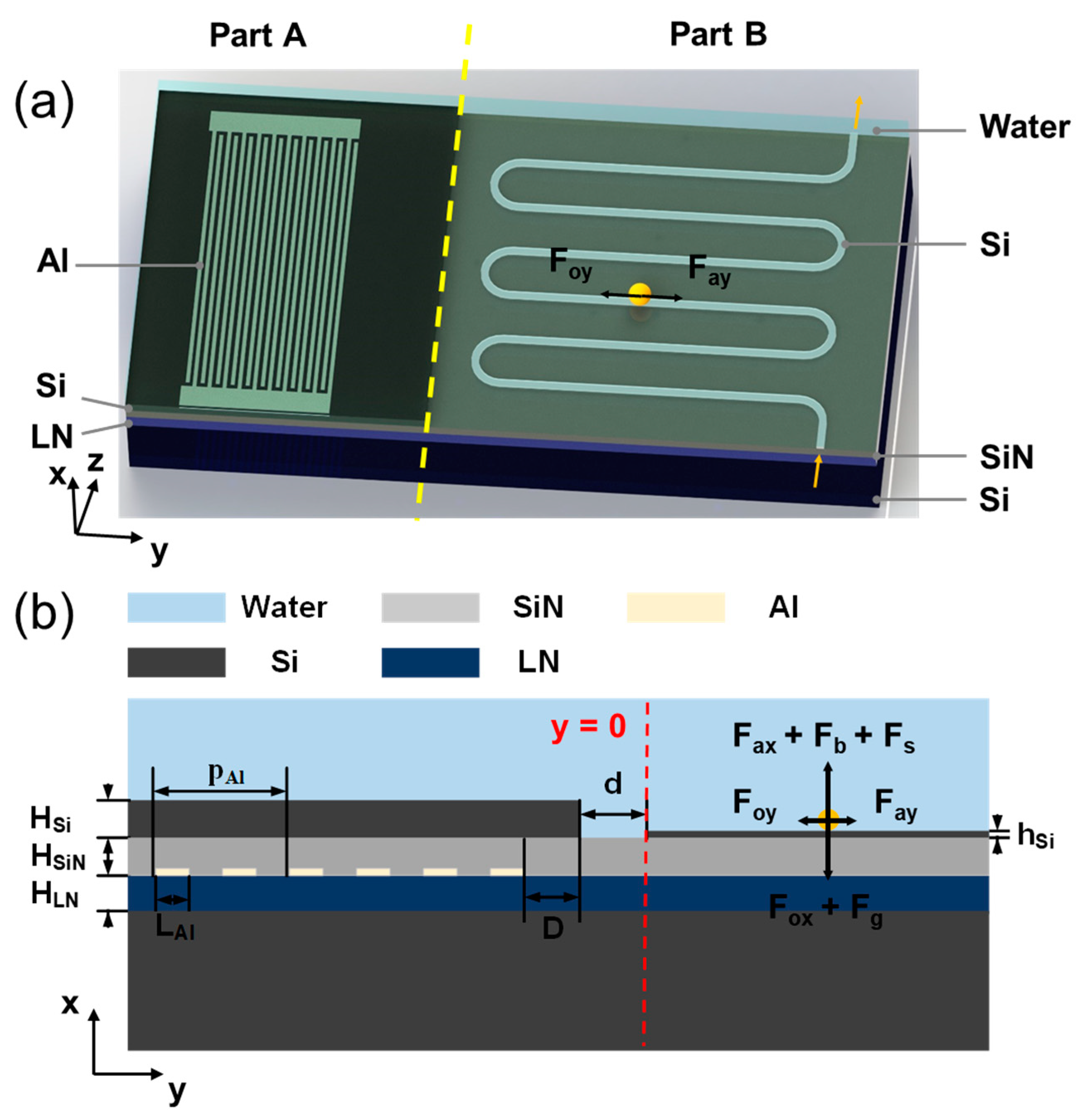
2. Principle and Model
3. Optical Force and Acoustic Force
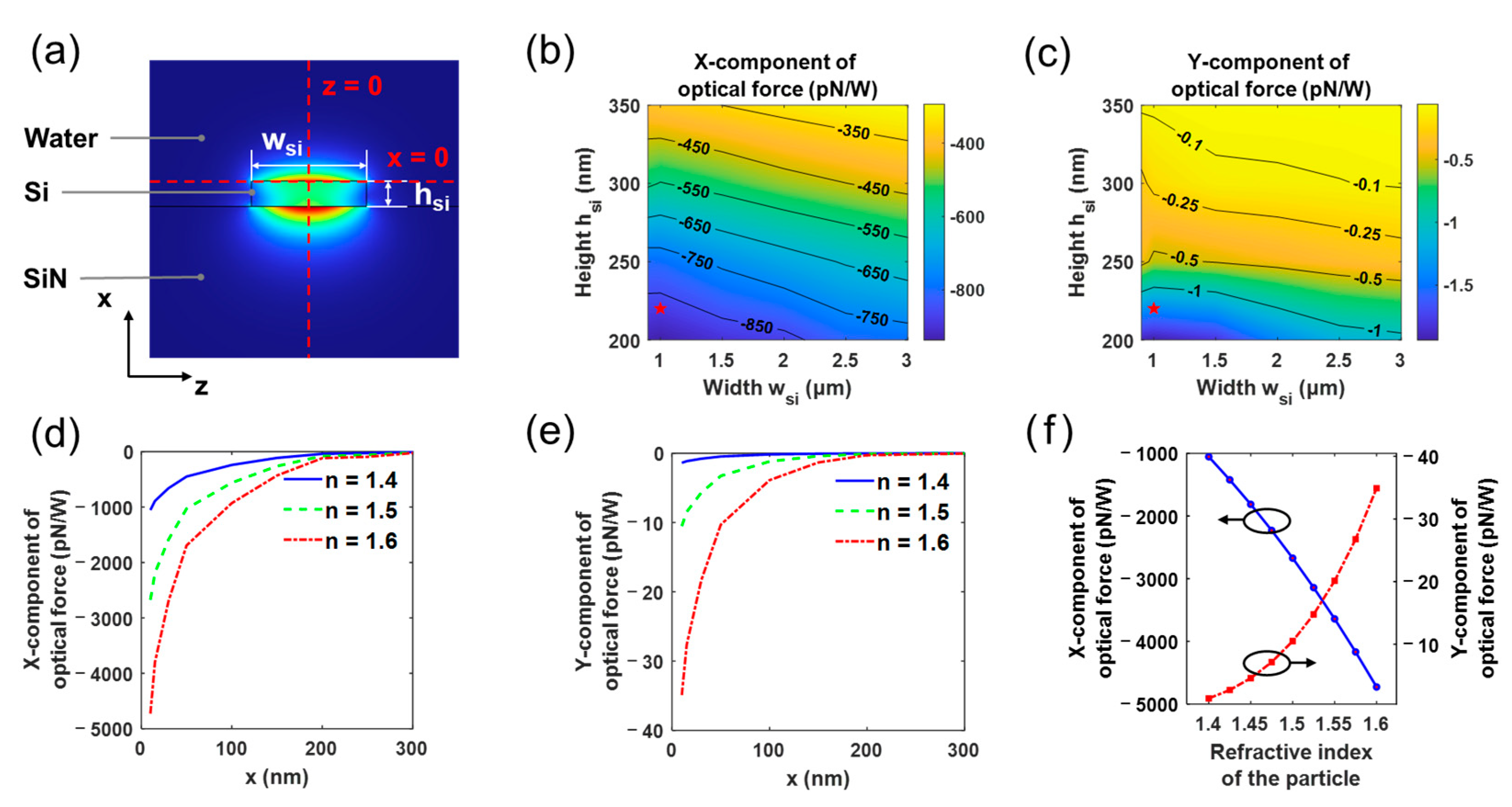
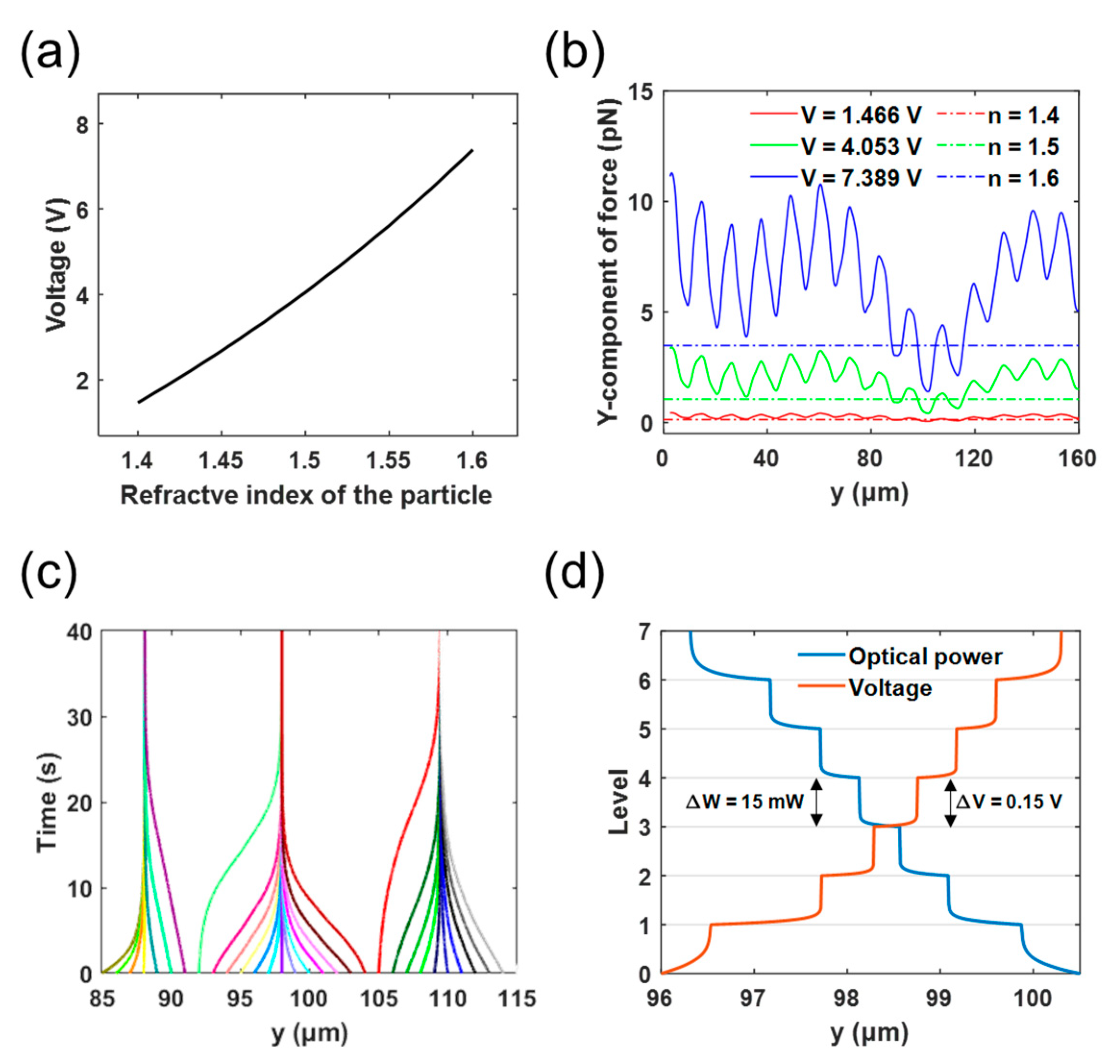
3.1. Optical Force
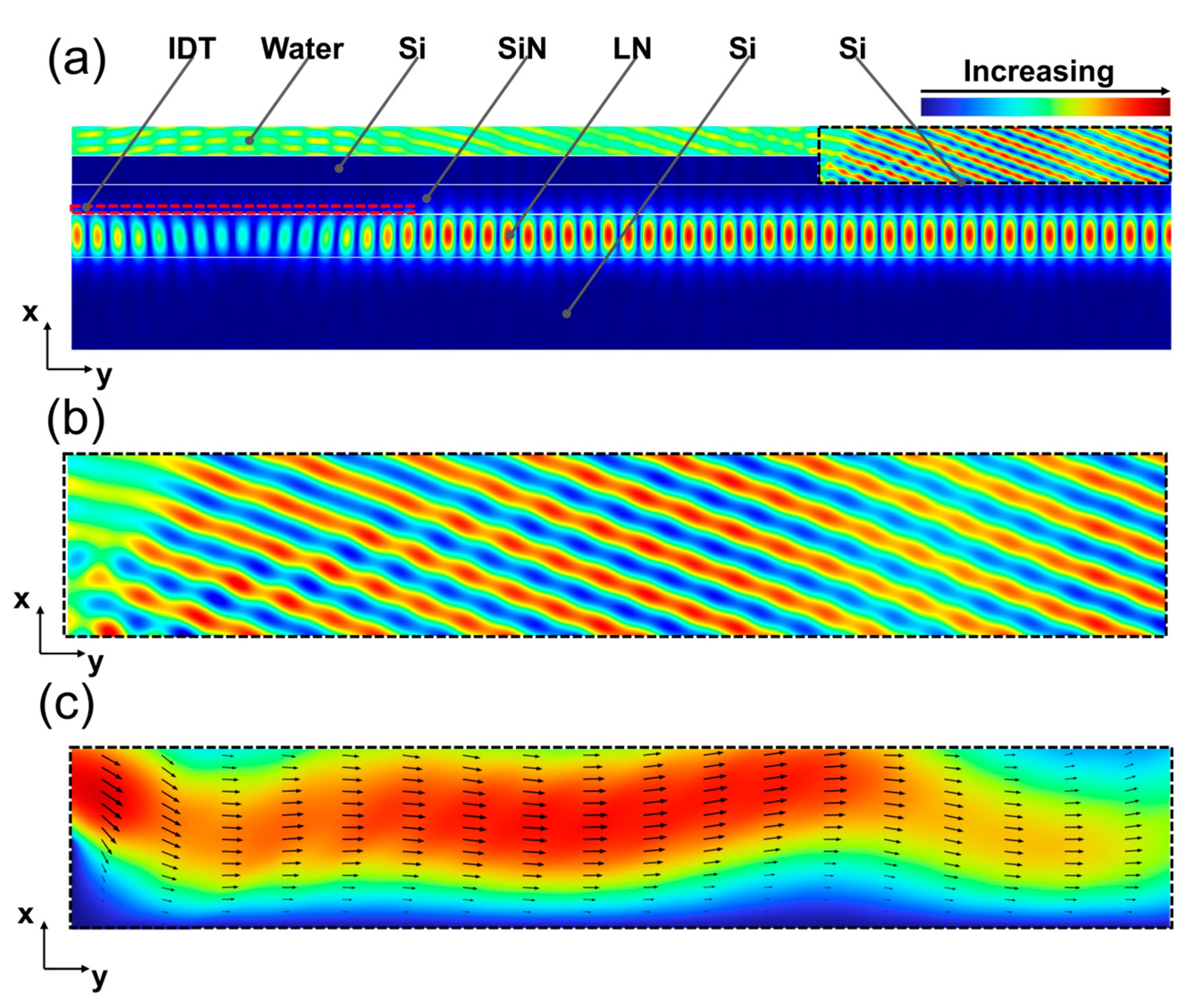
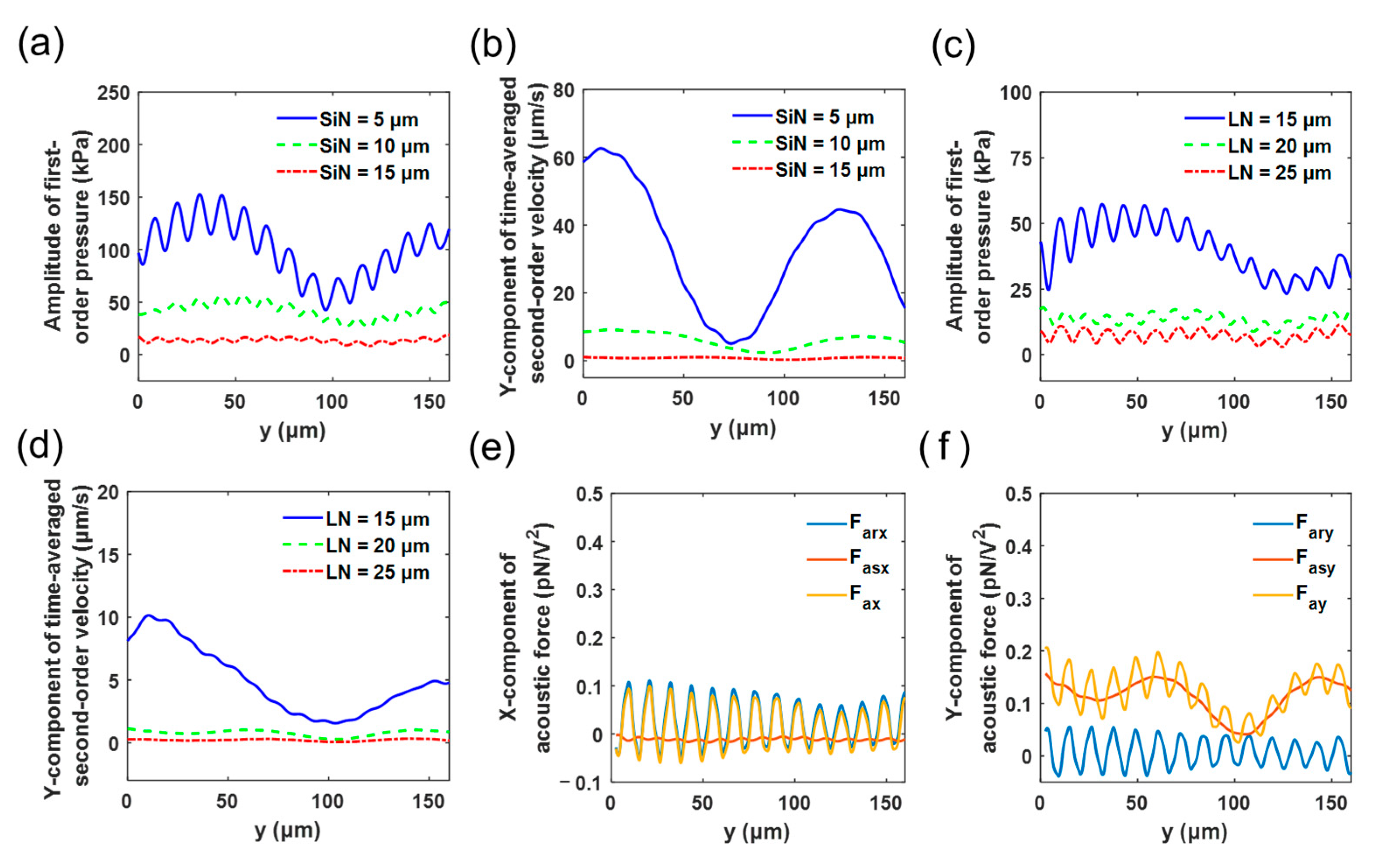
3.2. Acoustic Force
4. Dynamic Process of Trapping Particles
5. Discussion
6. Conclusions
Author Contributions
Funding
Institutional Review Board Statement
Informed Consent Statement
Data Availability Statement
Acknowledgments
Conflicts of Interest
References
- Badman, R.P.; Ye, F.; Wang, M.D. Towards Biological Applications of Nanophotonic Tweezers. Curr. Opin. Chem. Biol. 2019, 53, 158–166. [Google Scholar] [CrossRef] [PubMed]
- Zhao, X.T.; Zhao, N.; Shi, Y.; Xin, H.B.; Li, B.J. Optical Fiber Tweezers: A Versatile Tool for Optical Trapping and Manipulation. Micromachines 2020, 11, 114. [Google Scholar] [CrossRef] [PubMed]
- Meng, L.; Cai, F.; Li, F.; Zhou, W.; Niu, L.; Zheng, H. Acoustic Tweezers. J. Phys. D-Appl. Phys. 2019, 52, 273001. [Google Scholar] [CrossRef]
- Gaire, S.; Fabian, R.; Pegg, I.; Sarkar, A. Magnetic Tweezers: Development and Use in Single-Molecule Research. Biotechniques 2021, 72, 65–72. [Google Scholar] [CrossRef]
- Block, F.; Klingbeil, F.; Sajjad, U.; Arndt, C.; Sindt, S.; Seidler, D.; Thormählen, L.; Selhuber-Unkel, C.; McCord, J. Magnetic Bucket Brigade Transport Networks for Cell Transport. Adv. Mater. Technol. 2023, 8, 2300260. [Google Scholar] [CrossRef]
- Ghomian, T.; Hihath, J. Review of Dielectrophoretic Manipulation of Micro and Nanomaterials: Fundamentals, Recent Developments, and Challenges. IEEE Trans. Biomed. Eng. 2023, 70, 27–41. [Google Scholar] [CrossRef]
- Zhang, Y.; Min, C.; Dou, X.; Wang, X.; Urbach, H.P.; Somekh, M.G.; Yuan, X. Plasmonic Tweezers: For Nanoscale Optical Trapping and Beyond. Light-Sci. Appl. 2021, 10, 59. [Google Scholar] [CrossRef]
- Zhang, Y.; Tang, X.; Zhang, Y.; Liu, Z.; Zhao, E.; Yang, X.; Zhang, J.; Yang, J.; Yuan, L. Multiple Particles 3-D Trap Based on All-Fiber Bessel Optical Probe. J. Light. Technol. 2017, 35, 3849–3853. [Google Scholar] [CrossRef]
- Bhebhe, N.; Williams, P.A.C.; Rosales-Guzmán, C.; Rodriguez-Fajardo, V.; Forbes, A. A Vector Holographic Optical Trap. Sci. Rep. 2018, 8, 17387. [Google Scholar] [CrossRef]
- Chantakit, T.; Schlickriede, C.; Sain, B.; Meyer, F.; Weiss, T.; Chattham, N.; Zentgraf, T. All-Dielectric Silicon Metalens for Two-Dimensional Particle Manipulation in Optical Tweezers. Photonics Res. 2020, 8, 1435–1440. [Google Scholar] [CrossRef]
- Ahmad, A.; Dubey, V.; Singh, V.R.; Tinguely, J.-C.; Oie, C.I.; Wolfson, D.L.; Mehta, D.S.; So, P.T.C.; Ahluwalia, B.S. Quantitative Phase Microscopy of Red Blood Cells During Planar Trapping and Propulsion. Lab Chip 2018, 18, 3025–3036. [Google Scholar] [CrossRef] [PubMed]
- Sahafi, M.; Habibzadeh-Sharif, A. Robust Increase of the Optical Forces in Waveguide-Based Optical Tweezers Using V-Groove Structure. J. Opt. Soc. Am. B-Opt. Phys. 2018, 35, 1905–1909. [Google Scholar] [CrossRef]
- Wang, L.; Cao, Y.; Shi, B.; Li, H.; Feng, R.; Sun, F.; Lin, L.Y.; Ding, W. Subwavelength Optical Trapping and Transporting Using a Bloch Mode. Opt. Lett. 2020, 45, 1886–1889. [Google Scholar] [CrossRef] [PubMed]
- Ho, V.W.L.; Chang, Y.; Liu, Y.; Zhang, C.; Li, Y.; Davidson, R.R.; Little, B.E.; Wang, G.; Chu, S.T. Optical Trapping and Manipulating with a Silica Microring Resonator in a Self-Locked Scheme. Micromachines 2020, 11, 202. [Google Scholar] [CrossRef] [PubMed]
- Ye, F.; Inman, J.T.; Hong, Y.; Hall, P.M.; Wang, M.D. Resonator Nanophotonic Standing-Wave Array Trap for Single-Molecule Manipulation and Measurement. Nat. Commun. 2022, 13, 77. [Google Scholar] [CrossRef]
- Shi, Y.; Wu, Y.; Chin, L.K.; Li, Z.; Liu, J.; Chen, M.K.; Wang, S.; Zhang, Y.; Liu, P.Y.; Zhou, X.; et al. Multifunctional Virus Manipulation with Large-Scale Arrays of All-Dielectric Resonant Nanocavities. Laser Photon. Rev. 2022, 16, 2100197. [Google Scholar] [CrossRef]
- Ye, F.; Badman, R.P.; Inman, J.T.; Soltani, M.; Killian, J.L.; Wang, M.D. Biocompatible and High Stiffness Nanophotonic Trap Array for Precise and Versatile Manipulation. Nano Lett. 2016, 16, 6661–6667. [Google Scholar] [CrossRef]
- Li, H.; Yu, X.; Wu, X.; Shi, W.; Chen, M.; Liu, L.; Xu, L. All-Optically-Controlled Nanoparticle Transporting and Manipulating at Soi Waveguide Intersections. Opt. Express 2012, 20, 24160–24166. [Google Scholar] [CrossRef]
- Wang, J.; Poon, A.W. Unfolding a Design Rule for Microparticle Buffering and Dropping in Microring-Resonator-Based Add-Drop Devices. Lab Chip 2014, 14, 1426–1436. [Google Scholar] [CrossRef]
- Collins, D.J.; Ma, Z.; Han, J.; Ai, Y. Continuous Micro-Vortex-Based Nanoparticle Manipulation Via Focused Surface Acoustic Waves. Lab Chip 2016, 17, 91–103. [Google Scholar] [CrossRef]
- Tian, Z.; Yang, S.; Huang, P.-H.; Wang, Z.; Zhang, P.; Gu, Y.; Bachman, H.; Chen, C.; Wu, M.; Xie, Y.; et al. Wave Number–Spiral Acoustic Tweezers for Dynamic and Reconfigurable Manipulation of Particles and Cells. Sci. Adv. 2019, 5, eaau6062. [Google Scholar] [CrossRef]
- Zhang, P.; Chen, C.; Guo, F.; Philippe, J.; Gu, Y.; Tian, Z.; Bachman, H.; Ren, L.; Yang, S.; Zhong, Z.; et al. Contactless, Programmable Acoustofluidic Manipulation of Objects on Water. Lab Chip 2019, 19, 3397–3404. [Google Scholar] [CrossRef] [PubMed]
- Baudoin, M.; Gerbedoen, J.-C.; Riaud, A.; Matar, O.B.; Smagin, N.; Thomas, J.-L. Folding a Focalized Acoustical Vortex on a Flat Holographic Transducer: Miniaturized Selective Acoustical Tweezers. Sci. Adv. 2019, 5, eaav1967. [Google Scholar] [CrossRef] [PubMed]
- Kang, P.; Tian, Z.; Yang, S.; Yu, W.; Zhu, H.; Bachman, H.; Zhao, S.; Zhang, P.; Wang, Z.; Zhong, R.; et al. Acoustic Tweezers Based on Circular, Slanted-Finger Interdigital Transducers for Dynamic Manipulation of Micro-Objects. Lab Chip 2020, 20, 987–994. [Google Scholar] [CrossRef] [PubMed]
- De Vlaminck, I.; Dekker, C. Recent Advances in Magnetic Tweezers. Ann. Rev. Biophys. 2012, 41, 453–472. [Google Scholar] [CrossRef]
- Lin, P.T.; Chu, H.Y.; Lu, T.W.; Lee, P.T. Trapping Particles Using Waveguide-Coupled Gold Bowtie Plasmonic Tweezers. Lab Chip 2014, 14, 4647–4652. [Google Scholar] [CrossRef]
- Ashkin, A.; Dziedzic, J.M.; Bjorkholm, J.E.; Chu, S. Observation of a Single-Beam Gradient Force Optical Trap for Dielectric Particles. Opt. Lett. 1986, 11, 288–290. [Google Scholar] [CrossRef]
- Kawata, S.; Sugiura, T. Movement of Micrometer-Sized Particles in the Evanescent Field of a Laser Beam. Opt. Lett. 1992, 17, 772–774. [Google Scholar] [CrossRef]
- Soltani, M.; Lin, J.; Forties, R.A.; Inman, J.T.; Saraf, S.N.; Fulbright, R.M.; Lipson, M.; Wang, M.D. Nanophotonic Trapping for Precise Manipulation of Biomolecular Arrays. Nat. Nanotechnol. 2014, 9, 448–452. [Google Scholar] [CrossRef]
- Descharmes, N.; Dharanipathy, U.P.; Diao, Z.; Tonin, M.; Houdré, R. Observation of Backaction and Self-Induced Trapping in a Planar Hollow Photonic Crystal Cavity. Phys. Rev. Lett. 2013, 110, 123601. [Google Scholar] [CrossRef]
- van Leest, T.; Caro, J. Cavity-Enhanced Optical Trapping of Bacteria Using a Silicon Photonic Crystal. Lab Chip 2013, 13, 4358–4365. [Google Scholar] [CrossRef] [PubMed]
- O’Mahoney, P.; Brodie, G.W.; Wang, H.; Demore, C.E.M.; Cochran, S.; Spalding, G.C.; MacDonald, M.P. Hybrid Optical and Acoustic Force Based Sorting. In Proceedings of the Optical Trapping and Optical Micromanipulation XI, San Diego, CA, USA, 17–21 August 2014. [Google Scholar]
- Lovmo, M.K.; Pressl, B.; Thalhammer, G.; Ritsch-Marte, M. Controlled Orientation and Sustained Rotation of Biological Samples in a Sono-Optical Microfluidic Device. Lab Chip 2021, 21, 1563–1578. [Google Scholar] [CrossRef]
- Galanzha, E.I.; Viegas, M.G.; Malinsky, T.I.; Melerzanov, A.V.; Juratli, M.A.; Sarimollaoglu, M.; Nedosekin, D.A.; Zharov, V.P. In Vivo Acoustic and Photoacoustic Focusing of Circulating Cells. Sci. Rep. 2016, 6, 21531. [Google Scholar] [CrossRef] [PubMed]
- Fury, C.; Jones, P.H.; Memoli, G. Multiscale Manipulation of Microbubbles Employing Simultaneous Optical and Acoustical Trapping. In Proceedings of the Optical Trapping and Optical Micromanipulation XI, San Diego, CA, USA, 17–21 August 2014. [Google Scholar]
- Botter, R.; Ye, K.; Klaver, Y.; Suryadharma, R.; Daulay, O.; Liu, G.; van den Hoogen, J.; Kanger, L.; van der Slot, P.; Klein, E.; et al. Guided-Acoustic Stimulated Brillouin Scattering in Silicon Nitride Photonic Circuits. Sci. Adv. 2022, 8, eabq2196. [Google Scholar] [CrossRef]
- Edwards, R.L.; Coles, G.; Sharpe, W.N. Comparison of Tensile and Bulge Tests for Thin-Film Silicon Nitride. Exp. Mech. 2004, 44, 49–54. [Google Scholar] [CrossRef]
- Gyger, F.; Liu, J.; Yang, F.; He, J.; Raja, A.S.; Wang, R.N.; Bhave, S.A.; Kippenberg, T.J.; Thevenaz, L. Observation of Stimulated Brillouin Scattering in Silicon Nitride Integrated Waveguides. Phys. Rev. Lett. 2020, 124, 013902. [Google Scholar] [CrossRef] [PubMed]
- Ahmadi, S.; Hassani, F.; Korman, C.; Rahaman, M.; Zaghloul, M. Characterization of Multi- and Single-Layer Structure Saw Sensor. In Proceedings of the IEEE Sensors 2004 Conference, Vienna Univ Technol, Vienna, Austria, 24–27 October 2004. [Google Scholar]
- Chen, L.; Yang, C.; Xiao, Y.; Yan, X.; Hu, L.; Eggersdorfer, M.; Chen, D.; Weitz, D.A.; Ye, F. Millifluidics, Microfluidics, and Nanofluidics: Manipulating Fluids at Varying Length Scales. Mater. Today Nano 2021, 16, 100136. [Google Scholar] [CrossRef]
- Gao, J.M.; Carlier, J.; Wang, S.X.; Campistron, P.; Callens, D.; Guo, S.S.; Zhao, X.Z.; Nongaillard, B. Lab-on-a-Chip for High Frequency Acoustic Characterization. Sens. Actuator B-Chem. 2013, 177, 753–760. [Google Scholar] [CrossRef]
- Tong, X.; Tian, H.; Guo, Y.; Zhang, M.; Zhang, L. Dynamic Nanoparticle Trapping by Cascaded Nanophotonic Traps in a Silicon Slot Waveguide. IEEE J. Sel. Top. Quantum Electron. 2021, 27, 7300708. [Google Scholar] [CrossRef]
- Samandari, M.; Abrinia, K.; Sanati-Nezhad, A. Acoustic Manipulation of Bio-Particles at High Frequencies: An Analytical and Simulation Approach. Micromachines 2017, 8, 290. [Google Scholar] [CrossRef]
- Thomas, J.-L.; Marchiano, R.; Baresch, D. Acoustical and Optical Radiation Pressure and the Development of Single Beam Acoustical Tweezers. J. Quant. Spectrosc. Radiat. Transf. 2017, 195, 55–65. [Google Scholar] [CrossRef]
- Muller, P.B.; Barnkob, R.; Jensen, M.J.H.; Bruus, H. A Numerical Study of Microparticle Acoustophoresis Driven by Acoustic Radiation Forces and Streaming-Induced Drag Forces. Lab Chip 2012, 12, 4617–4627. [Google Scholar] [CrossRef]
- Zhao, H.T.; Chin, L.K.; Shi, Y.Z.; Liu, P.Y.; Zhang, Y.; Cai, H.; Yap, E.P.H.; Ser, W.; Liu, A.Q. Continuous Optical Sorting of Nanoscale Biomolecules in Integrated Microfluidic-Nanophotonic Chips. Sens. Actuator B-Chem. 2021, 331, 129428. [Google Scholar] [CrossRef]
- Gaugiran, S.; Gétin, S.; Fedeli, J.M.; Colas, G.; Fuchs, A.; Chatelain, F.; Dérouard, J. Optical Manipulation of Microparticles and Cells on Silicon Nitride Waveguides. Opt. Express 2005, 13, 6956–6963. [Google Scholar] [CrossRef] [PubMed]
- Ross, K.F.; Billing, E. The Water and Solid Content of Living Bacterial Spores and Vegetative Cells as Indicated by Refractive Index Measurements. J. Gen. Microbiol. 1957, 16, 418–425. [Google Scholar] [CrossRef]
- Salim, Z.T.; Hashim, U.; Arshad, M.K.M. Fem Modeling and Simulation of a Layered Saw Device Based on Zno/128° Yx Linbo3. In Proceedings of the 2016 IEEE International Conference on Semiconductor Electronics (ICSE), Kaula Lumpur, Malaysia, 17–19 August 2016. [Google Scholar]
- Namdeo, A.K.; Nemade, H.B. Simulation on Effects of Electrical Loading Due to Interdigital Transducers in Surface Acoustic Wave Resonator. In Proceedings of the International Conference On Design and Manufacturing (IConDM), IIITDM Kancheepuram, Chennai, India, 18–20 July 2013. [Google Scholar]
- Kim, H.J.; Yang, W.S.; No, K. Improvement of Low-Frequency Characteristics of Piezoelectric Speakers Based on Acoustic Diaphragms. IEEE Trans. Ultrason. Ferroelectr. Freq. Control 2012, 59, 2027–2035. [Google Scholar] [CrossRef] [PubMed]
- Wu, Y.; Chattaraj, R.; Ren, Y.; Jiang, H.; Lee, D. Label-Free Multitarget Separation of Particles and Cells under Flow Using Acoustic, Electrophoretic, and Hydrodynamic Forces. Anal. Chem. 2021, 93, 7635–7646. [Google Scholar] [CrossRef]
- Cardenas, J.; Poitras, C.B.; Luke, K.; Luo, L.W.; Morton, P.A.; Lipson, M. High Coupling Efficiency Etched Facet Tapers in Silicon Waveguides. IEEE Photonics Technol. Lett. 2014, 26, 2380–2382. [Google Scholar] [CrossRef]
- Cai, H.; Poon, A.W. Optical Trapping of Microparticles Using Silicon Nitride Waveguide Junctions and Tapered-Waveguide Junctions on an Optofluidic Chip. Lab Chip 2012, 12, 3803–3809. [Google Scholar] [CrossRef]
- Song, F.; Xiao, J.; Seo, S.-W. Heterogeneously Integrated Optical System for Lab-on-a-Chip Applications. Sens. Actuator A Phys. 2013, 195, 148–153. [Google Scholar] [CrossRef]
- Angelsky, O.; Maksymyak, P.; Zenkova, C.; Maksymyak, A.; Hanson, S.; Ivanskyi, D. Peculiarities of Control of Erythrocytes Moving in an Evanescent Field. J. Biomed. Opt. 2019, 24, 055002. [Google Scholar] [CrossRef] [PubMed]
- Jinan Jingzheng Electronics Co. Ltd. Available online: https://www.nanoln.com/ (accessed on 8 September 2023).
- Kumar, A.; Prasad, M.; Janyani, V.; Yadav, R.P. Development of Diaphragm and Microtunnel Structures for Mems Piezoelectric Sensors. IEEE Trans. Semicond. Manuf. 2020, 33, 606–613. [Google Scholar] [CrossRef]
- Kaloyeros, A.E.; Jové, F.A.; Goff, J.; Arkles, B. Review—Silicon Nitride and Silicon Nitride-Rich Thin Film Technologies: Trends in Deposition Techniques and Related Applications. ECS J. Solid State Sci. Technol. 2017, 6, P691–P714. [Google Scholar] [CrossRef]
- Tuncer, E. Nonlinear Conductivity in Silicon Nitride. Solid-State Electron. 2017, 134, 46–50. [Google Scholar] [CrossRef]
- Yeghoyan, T.; Alassaad, K.; Soulière, V.; Douillard, T.; Carole, D.; Ferro, G. Growth and Characterization of Undoped Polysilicon Thick Layers: Revisiting an Old System. Silicon 2020, 12, 1187–1194. [Google Scholar] [CrossRef]
- Vanhove, E.; Tsopéla, A.; Bouscayrol, L.; Desmoulin, A.; Launay, J.; Temple-Boyer, P. Final Capping Passivation Layers for Long-Life Microsensors in Real Fluids. Sens. Actuator B-Chem. 2013, 178, 350–358. [Google Scholar] [CrossRef]
- Zhang, Y.; Yang, S.Y.; Lim, A.E.J.; Lo, G.Q.; Galland, C.; Baehr-Jones, T.; Hochberg, M. A Cmos-Compatible, Low-Loss, and Low-Crosstalk Silicon Waveguide Crossing. IEEE Photonics Technol. Lett. 2013, 25, 422–425. [Google Scholar] [CrossRef]

| Type of Tweezer | Tweezer Composition | Captured Particle | Type of Force | Feature | Reference |
|---|---|---|---|---|---|
| Free-space optical tweezer | The optical fiber | Yeast cells | Optical force | Multiple yeast cells 3D stable trapping | [8] |
| The holographic lens group | 2 μm diameter silica beads | Optical force | The 3D shape control of the optical forces | [9] | |
| The metasurface | Polystyrene particles with a diameter of 4.5 μm | Optical force | Polarization-sensitive 2D manipulation | [10] | |
| Near-field optical tweezer | The strip and rib waveguides | Red blood cells | Optical force | Developing a methodology for quantitatively studying red blood cells | [11] |
| The V-groove waveguide | Polystyrene nanoparticles | Optical force | The much higher capability to trap nanoparticles | [12] | |
| The one-dimensional (1D) photonic crystal waveguide | The polystyrene particle with a refractive index of 1.56 and a radius of 150 nm | Optical force | Efficient optical trapping and transportation in a peristaltic way | [13] | |
| The microring resonator | Polystyrene beads of sizes up to 3 µm | Optical force | The trapping capability maintaining based on the self-locked scheme | [14] | |
| The resonator and nanophotonic standing-wave array | 380 nm polystyrene beads | Optical force | Significant force enhancement and base-pair resolution measurements of multiple molecules | [15] | |
| The photonic crystal cavity | Viruses with diameters ranging from 20 to 100 nm and RI of 1.4 (virus) and 1.58 (polystyrene nanoparticle) | Optical force | Single or massive virus transporting, positioning, patterning, sorting, and concentrating | [16] | |
| Acoustic tweezer | The piezoelectric transducer | The 10 μm polystyrene bead | Acoustic force | Dynamic wavefields reshaping and dynamic and reconfigurable particle/cell manipulation | [21] |
| The piezoelectric transducer | The zebrafish larvae and oil droplets | Acoustic force | The digital actuation of small objects on the surface of water | [22] | |
| The flat holographic transducer | Polystyrene particles with a radius of 75 ± 2 μm | Acoustic force | Selectively trapping and moving for one particle independently | [23] | |
| The circular, slanted-finger piezoelectric transducer | 10.2 μm yellow-green polystyrene microspheres and K562 cells | Acoustic force | Dynamic and reconfigurable manipulations of microparticles and cells | [24] | |
| Hybrid tweezer | The holographic lens group (free-space) and piezoelectric transducer | Polystyrene and silica spheres | Optical and acoustic forces | Optical sorting and acoustic trapping | [32] |
| The holographic lens group (free-space) and piezoelectric transducer | Micro-organisms | Optical and acoustic forces | Controlled reorientation and controlled continuous rotation of specimens | [33] | |
| The rectangle waveguide (near-field integrated) and piezoelectric transducer | The particle with a refractive index of 1.4 and a diameter of 5 μm (similar to yeast cells) | Optical and acoustic forces | Particle capturing, controlled reorientation, and the separation of particles with significantly different refractive indices | This work |
| Symbol | Notation |
|---|---|
| The optical force | |
| The total acoustic force | |
| The acoustic radiation force | |
| The Stokes drag force | |
| The gravity of the particle | |
| The buoyancy of the particle | |
| The supporting force | |
| The Maxwell stress tensor | |
| The normal vector | |
| The surface of the particle | |
| The electric field | |
| The electric displacement | |
| The magnetic field | |
| The magnetic flux field | |
| The isotropy tensor | |
| The Brillouin stress tensor | |
| The density of water | |
| The i-th direction component of the first-order velocity | |
| The first-order pressure | |
| The speed of sound in water | |
| The Kronecker delta | |
| The viscosity of water | |
| The radius of particle | |
| The second-order velocity of water | |
| The velocity of the particle | |
| The distance between the center of the particle and the surface | |
| The mass of the particle | |
| The acceleration of the particle |
| HSi | HSiN | HLN | λ | LAl | pAl | D | d | wSi | hSi |
|---|---|---|---|---|---|---|---|---|---|
| 15 | 15 | 20 | 20.5 | 5.125 | 20.5 | 272.9 | 20 | 1 | 0.22 |
Disclaimer/Publisher’s Note: The statements, opinions and data contained in all publications are solely those of the individual author(s) and contributor(s) and not of MDPI and/or the editor(s). MDPI and/or the editor(s) disclaim responsibility for any injury to people or property resulting from any ideas, methods, instructions or products referred to in the content. |
© 2023 by the authors. Licensee MDPI, Basel, Switzerland. This article is an open access article distributed under the terms and conditions of the Creative Commons Attribution (CC BY) license (https://creativecommons.org/licenses/by/4.0/).
Share and Cite
Li, S.; Tong, X.; Cai, L.; Zhang, L. Integrated Hybrid Tweezer for Particle Trapping with Combined Optical and Acoustic Forces. Appl. Sci. 2023, 13, 10673. https://doi.org/10.3390/app131910673
Li S, Tong X, Cai L, Zhang L. Integrated Hybrid Tweezer for Particle Trapping with Combined Optical and Acoustic Forces. Applied Sciences. 2023; 13(19):10673. https://doi.org/10.3390/app131910673
Chicago/Turabian StyleLi, Sen, Xin Tong, Lutong Cai, and Lin Zhang. 2023. "Integrated Hybrid Tweezer for Particle Trapping with Combined Optical and Acoustic Forces" Applied Sciences 13, no. 19: 10673. https://doi.org/10.3390/app131910673