
Perspective of Using Vertically Oriented Graphene as an Electrochemical Biosensing Platform

Abstract
:1. Introduction
2. Materials and Methods
2.1. Synthesis of VG
2.2. Characterization Methods
3. Results and Discussions
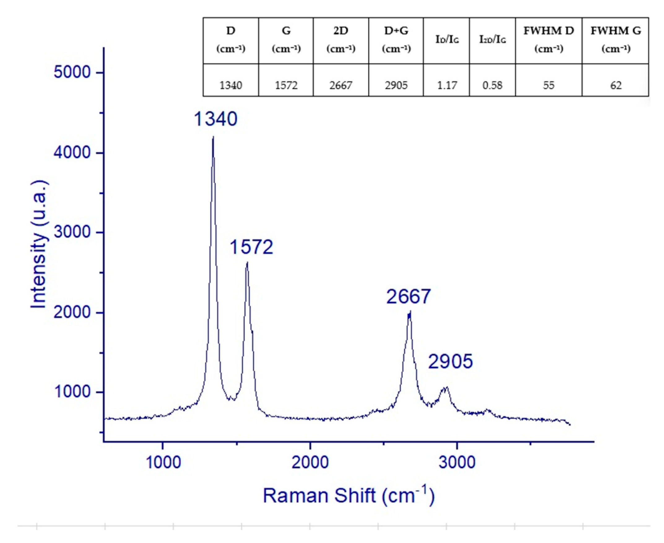
3.1. Raman Spectroscopy
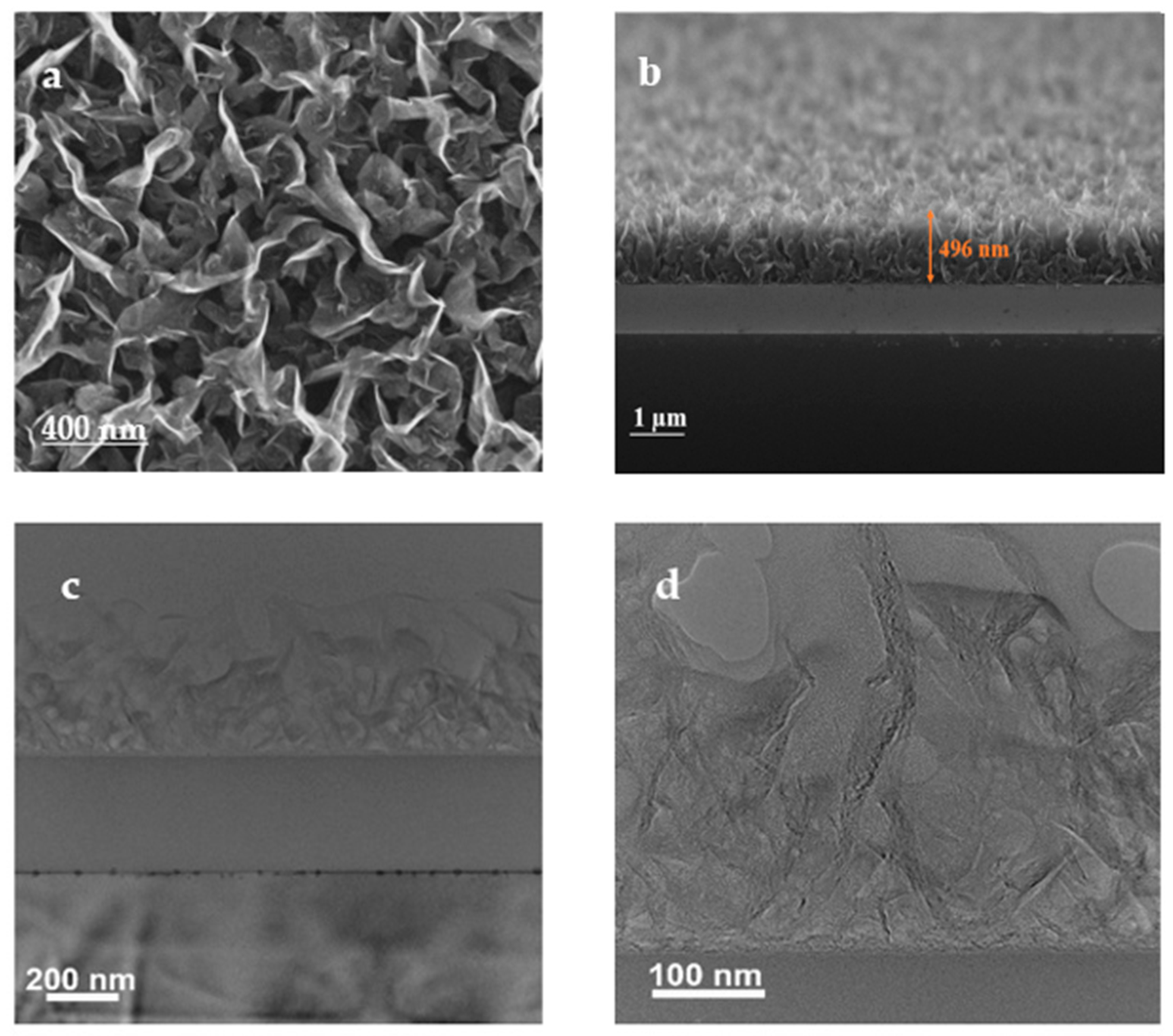
3.2. SEM and TEM Analysis
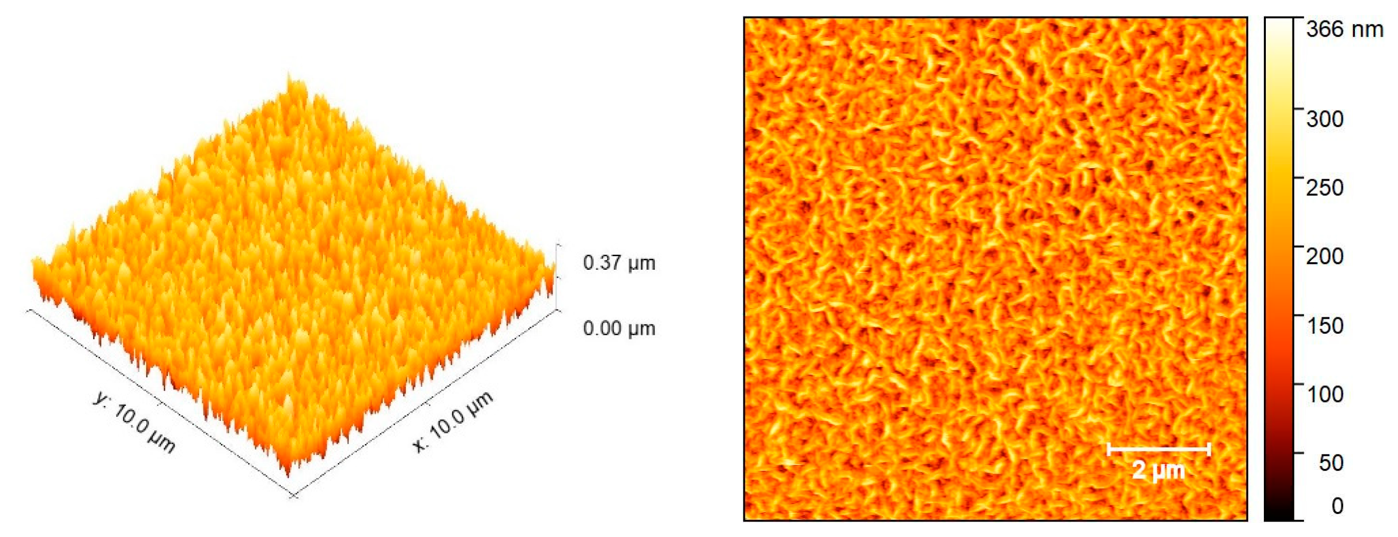
3.3. AFM Analysis
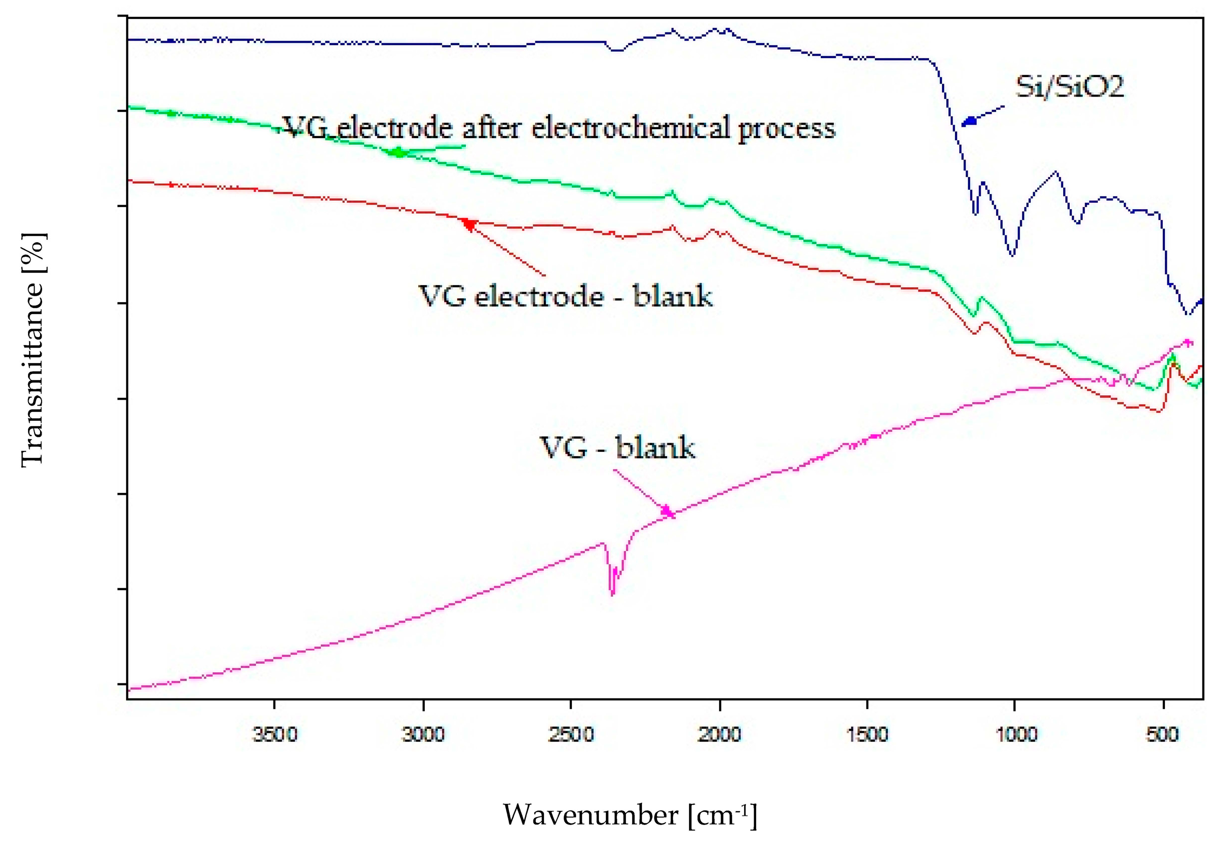
3.4. FTIR Analysis
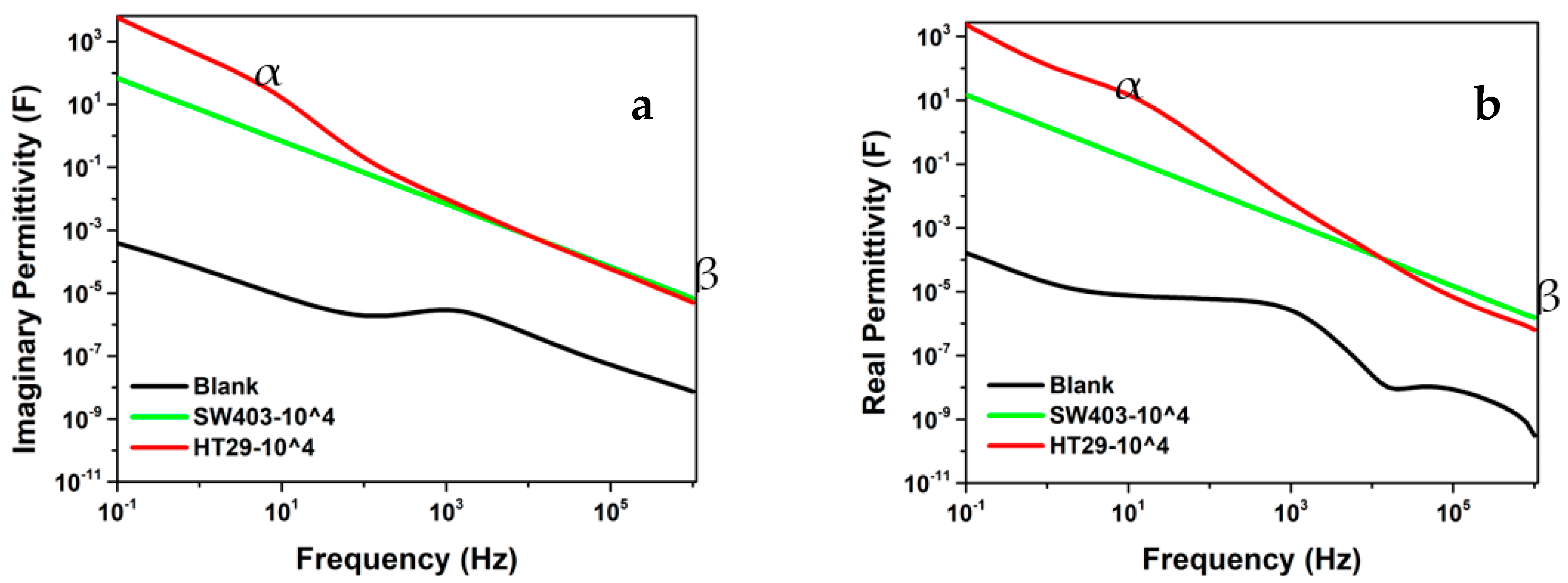
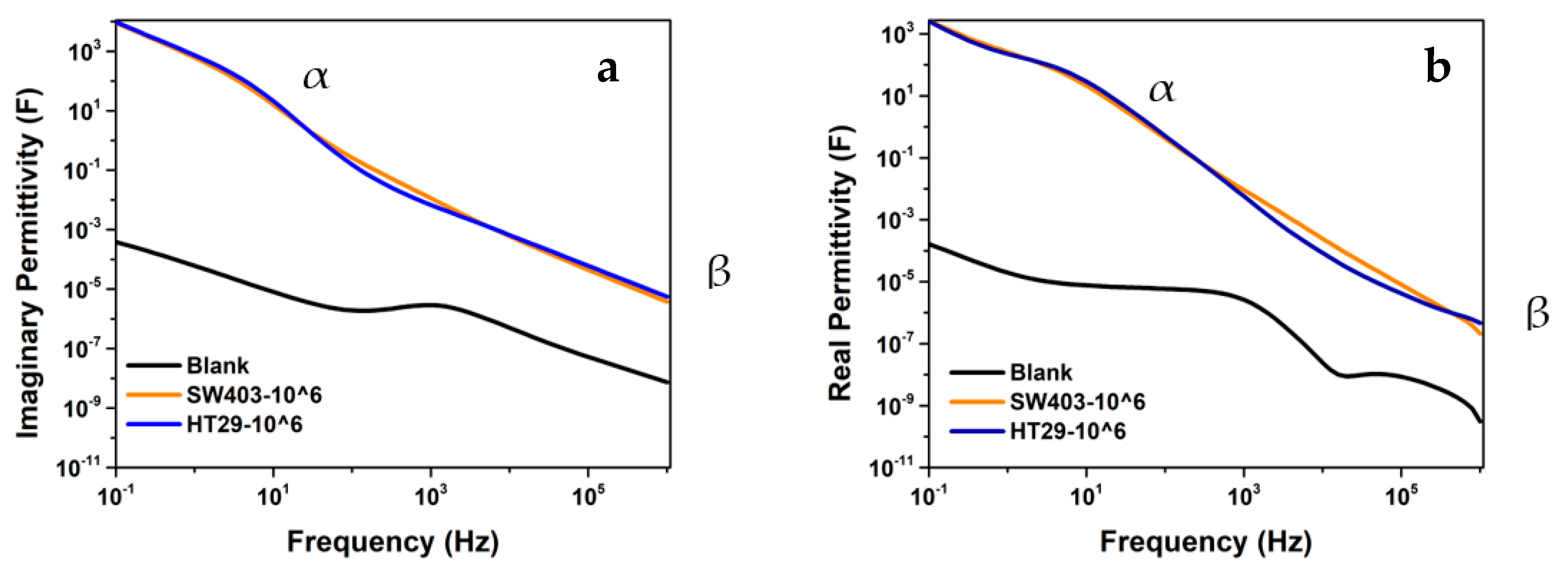
3.5. EIS Analysis
4. Conclusions
Author Contributions
Funding
Acknowledgments
Conflicts of Interest
References
- Junhong, C.; Zheng, B.; Ganhua, L. Vertically-Oriented Graphene: PECVD Synthesis and Applications, 1st, ed.; Springer: Cham, Switzerland, 2015. [Google Scholar] [CrossRef]
- Cao, X.; Shi, Y.; Shi, W.; Lu, G.; Huang, X. Vertically oriented graphene materials: Synthesis, characterizations, and applications. Small 2017, 13, 1701976. [Google Scholar]
- Zhang, Y.; Wang, X.; Wu, H.; Zhou, C. Vertically oriented graphene-based materials: Synthesis, characterization, and applications. Adv. Mater. 2015, 27, 7493–7527. [Google Scholar]
- Anghel, E.; Adiaconita, B.; Demetrescu, I.; Avram, A. A Review of Vertical Graphene and Its Biomedical Applications. Coatings 2023, 13, 761. [Google Scholar] [CrossRef]
- Ren, J.; Han, J.; Ma, Y.; Wang, M.; Tong, Z.; Suhr, J.; Xiao, L.; Jia, S.; Chen, X. Morphology and surface engineering of vertical graphene films for dye photodegradation. Ceram. Int. 2022, 48, 9477–9482. [Google Scholar] [CrossRef]
- Zheng, W.; Zhao, X.; Fu, W. Review of Vertical Graphene and its Applications. ACS Appl. Mater. Interfaces 2021, 13, 9561–9579. [Google Scholar] [CrossRef] [PubMed]
- Ih, C.; Lee, J.; Kim, J.; Kang, M.S.; Paik, J.K.; Ku, S. Current technologies of electrochemical immunosensors: Perspective on signal amplification. Sensors 2018, 18, 207. [Google Scholar]
- Bahamonde, J.P.; Nguyen, H.N.; Fanourakis, S.K.; Rodrigues, D.F. Recent advances in graphene-based biosensor technology with applications in life sciences. J. Nanobiotechnol. 2018, 16, 75. [Google Scholar]
- Liu, A.; Wang, K.; Weng, S.; Lei, Y.; Lin, L.; Chen, W. Development of electrochemical DNA biosensors. Trends Anal. Chem. 2012, 37, 101–111. [Google Scholar] [CrossRef]
- Wang, Y.; Shao, Y.; Matson, D.W.; Li, J.; Lin, Y. Nitrogen-doped graphene and its application in electrochemical biosensing. ACS Nano 2010, 4, 1790–1798. [Google Scholar] [CrossRef]
- Chen, L.F.; Zhang, X.D.; Liang, H.W.; Kong, M.G.; Cui, Z.D.; Png, R.Q.; Chen, P. High performance three-dimensional tubular array based on nitrogen-doped graphene for high-rate supercapacitors. ACS Nano 2012, 6, 9132–9141. [Google Scholar]
- Patiño, T.; Souto DE, P.; Lopes JM, J.; Chaves, A.R.; Machado SA, S.; Kubota, L.T. Electrochemical genosensing platform based on graphene oxide for detection of short DNA sequences related to the human T-cell lymphotropic virus. Sens. Actuators B Chem. 2018, 254, 808–814. [Google Scholar]
- Mao, S.; Yu, K.; Chang, J.; Steeber, D.A.; Ocola, L.E.; Chen, J. Direct Growth of Vertically-oriented Graphene for Field-Effect Transistor Biosensor. Sci. Rep. 2013, 3, 1696. [Google Scholar] [CrossRef]
- Chen, Q.; Sun, T.; Song, X.; Ran, Q.; Yu, C.; Yang, J.; Feng, H.; Yu, L.; We, D. Flexible electrochemical biosensors based on graphene nanowalls for the real-time measurement of lactate. Nanotechnology 2017, 28, 315501. [Google Scholar] [CrossRef]
- Tzouvadaki, I.; Aliakbarinodehi, N.; Pineda, D.D.; De Micheli, G.; Carrara, S. Graphene nanowalls for high-performance chemotherapeutic drug sensing and anti-fouling properties. Sens. Actuators B Chem. 2018, 262, 395–403. [Google Scholar] [CrossRef]
- Li, Y.; Liu, X.; Li, M.; Liu, Q.; Xu, T. Portable Vertical Graphene@Au-Based Electrochemical Aptasensing Platform for Point-of-Care Testing of Tau Protein in the Blood. Biosensors 2022, 12, 564. [Google Scholar] [CrossRef] [PubMed]
- Abolpour, M.; Azadi, S.; Belford, A.; Razmjou, A.; Wu, S.; Han, Z.; Asadnia, M. Development of an Ultra-Sensitive and Flexible Piezoresistive Flow Sensor Using Vertical Graphene Nanosheets. Nano-Micro Lett. 2020, 12, 109. [Google Scholar] [CrossRef] [PubMed]
- Burinaru, T.; Adiaconita, B.; Avram, M.; Preda, P.; Enciu, A.M.; Chiriac, E.; Marculescu, C.; Constantin, T. Electrochemical impedance spectroscopy based microfluidic biosensor for the detection of circulating tumor cells. Mater. Today Commun. 2022, 32, 104016. [Google Scholar] [CrossRef]
- Tincu, B.; Burinaru, T.; Enciu, A.M.; Preda, P.; Chiriac, E.; Marculescu, C.; Avram, M.; Avram, A. Vertical Graphene-Based Biosensor for Tumor Cell Dielectric Signature Evaluation. Micromachines 2022, 13, 1671. [Google Scholar] [CrossRef]
- Anghel, E.; Adiaconita, B.; Avram, A.; Mihailescu, C.; Pachiu, C.; Brincoveanu, O.; Popescu, R.C.; Demetrescu, I. Vertical graphene growth process optimization for use in cellular identification. Bull. Mater. Sci. 2023, 46, 105. [Google Scholar] [CrossRef]
- Mishra, K.K.; Ghosh, S.; Thoguluva, R.; Amirthapandian, S.; Kamruddin, M. Thermal conductivity and pressure-dependent Raman studies of vertical graphene nanosheets. J. Phys. Chem. C 2016, 120, 4. [Google Scholar] [CrossRef]


| Sample | Rs (Ω) | Rp (Ω) | Rct (Ω) | Z″max (Ω) | Cdl (μF) |
|---|---|---|---|---|---|
| VG | 53.8 | 2630 | 1474 | 1237 | 5.98 |
| SW 403—104 cells/mL | 32.8 | 6071 | 3250 | 2921 | 6.38 |
| HT 29—104 cells/mL | 49.9 | 4071 | 1190 | 905 | 5.66 |
| SW 403—106 cells/mL | 29.9 | 5236 | 2787 | 1825 | 8.92 |
| HT 29—106 cells/mL | 39.4 | 5380 | 2409 | 1999 | 4.85 |
Disclaimer/Publisher’s Note: The statements, opinions and data contained in all publications are solely those of the individual author(s) and contributor(s) and not of MDPI and/or the editor(s). MDPI and/or the editor(s) disclaim responsibility for any injury to people or property resulting from any ideas, methods, instructions or products referred to in the content. |
© 2023 by the authors. Licensee MDPI, Basel, Switzerland. This article is an open access article distributed under the terms and conditions of the Creative Commons Attribution (CC BY) license (https://creativecommons.org/licenses/by/4.0/).
Share and Cite
Anghel, E.; Adiaconita, B.; Avram, A.; Demetrescu, I. Perspective of Using Vertically Oriented Graphene as an Electrochemical Biosensing Platform. Appl. Sci. 2023, 13, 11833. https://doi.org/10.3390/app132111833
Anghel E, Adiaconita B, Avram A, Demetrescu I. Perspective of Using Vertically Oriented Graphene as an Electrochemical Biosensing Platform. Applied Sciences. 2023; 13(21):11833. https://doi.org/10.3390/app132111833
Chicago/Turabian StyleAnghel, Elena, Bianca Adiaconita, Andrei Avram, and Ioana Demetrescu. 2023. "Perspective of Using Vertically Oriented Graphene as an Electrochemical Biosensing Platform" Applied Sciences 13, no. 21: 11833. https://doi.org/10.3390/app132111833