Article

Air-Stable Near-Infrared Sensitive Organic Phototransistors Realized via Tri-Layer Planar Heterojunction

1
School of Electronic and Information Engineering, Lanzhou Jiaotong University, Lanzhou 730070, China
2
School of Mechanical Engineering, Lanzhou Jiaotong University, Lanzhou 730070, China
3
Engineering Research Center of Integrated Circuit Packaging and Testing, Ministry of Education, Tianshui 741000, China
4
School of Electronic Information and Electrical Engineering, Tianshui Normal University, Tianshui 741000, China
*
Author to whom correspondence should be addressed.
Appl. Sci. 2023, 13(23), 12613; https://doi.org/10.3390/app132312613
Submission received: 12 October 2023 / Revised: 12 November 2023 / Accepted: 15 November 2023 / Published: 23 November 2023

Abstract

:
Near-infrared (NIR) light has many applications in agriculture, transportation, medicine, the military, and other fields. Lead phthalocyanine (PbPc) exhibits excellent near-infrared (NIR) light absorption characteristics and is widely used in NIR-sensitive organic photodetectors. In this work, PbPc-based NIR organic phototransistors (OPTs) with different active layer structures were designed and fabricated. The photo-absorption characteristics of organic films, photosensitive properties, and air stability of the devices were investigated. The results suggested that (i) the bilayer planar heterojunction (PHJ) devices exhibit far better photosensitive performance than the single layer ones due to higher mobility of the formers than the latters; (ii) the bilayer PHJ ones with p-type channel have equivalent photosensitive performance to those with n-type channel owing to equivalent mobility, higher NIR absorption and lower exciton dissociation efficiency of the formers than the latters; (iii) the bilayer PHJ ones with p-type channel possess superior air stability to those with n-type channel thanks to better air stability of pentacene channel layer than C60 channel layer; (iv) the tri-layer PHJ ones perform better than the bilayer PHJ ones with p-type channel and exhibit a high photoresponsivity of 1415 mA/W and a maximum photo-to-dark current ratio of 1.2 × 10⁴, and such an outstanding performance benefits from the virtues of tri-layer PHJ structure including high light absorption, carrier mobility and exciton dissociation efficiency; and (v) the air stability of the tri-layer PHJ ones is better than that of the bilayer PHJ ones with p-type channel, which can be attributed to the passivation of the top-level C60 layer.

1. Introduction

In industry, agriculture, transportation, medicine, the military, and various other fields [1,2,3,4], near-infrared (NIR) light serves a significant purpose. The detection of NIR light has attracted considerable attention, leading to extensive research on developing NIR-sensitive devices [5,6,7,8]. Organic NIR photodetectors are gaining increasing recognition for their extensive applications in sensing and imaging [9,10]. While traditional inorganic alternatives have seen widespread application, they still present certain limitations. For instance, some NIR photodetectors rely on narrow-bandgap semiconductors like InGaAs, which necessitate cooling for optimal operation to suppress intrinsic carrier concentration. This cooling requirement complicates the routine use of these devices. In contrast, organic photodetectors offer distinct advantages compared to their inorganic counterparts, including cost-effective production, the ability for large-area fabrication, and excellent mechanical flexibility [11,12,13,14,15]. Furthermore, there exists a wide array of materials to choose from.
To create efficient organic NIR photodetectors, specific properties are necessary in the organic NIR-sensitive materials. These properties include a low band gap, exceptional thermal and chemical stability, and strong absorption within the NIR region. Among the various materials considered, metal phthalocyanines have garnered significant attention for their role as active components in organic solar cells, organic photodiodes (OPDs), and organic field-effect transistors [16,17,18]. These metal phthalocyanines include zinc phthalocyanine, lead phthalocyanine (PbPc), and neodymium phthalocyanine, and so on [19,20,21]. Among them, PbPc is drawing intense interest in organic optoelectronic devices due to its nice NIR absorption and semiconductor characteristics [20,21,22]. Organic phototransistors (OPTs) represent a category of light-detecting transistors with the unique capability of optical control over their channel conductance. OPTs typically exhibit a superior photo-to-dark current ratio and reduced noise levels compared to organic photodiodes (OPDs) [23], making them the primary focus of our investigation. In the realm of OPTs, the performance of OPTs is notably influenced by three critical factors: light absorption, transport of channel carriers, and exciton dissociation efficiency. It becomes a hot issue to realize high light absorption, carrier transport, and exciton dissociation efficiency in a discrete OPT. Conventional single-layer OPTs are often unable to attain the above objectives. For this, some effective methods, such as heterojunction structures, interfacial modification, and nanomaterial doping, are put forward and adopted to solve this problem. Among these methods, heterojunction structures (e.g., planar heterojunction (PHJ), bulk heterojunction) are paid more attention by researchers due to their advantages, such as flexible designs, easy realization, and favorable performance. High carrier mobility, light absorption, and exciton dissociation efficiency can be achieved in a single device by using heterojunction structures. Especially, it is found that the NIR absorption of the photoactive layer in a PHJ structure can be enhanced due to template inducing of the underneath organic function layer (e.g., pentacene and copper phthalocyanine channel layer). Binda et al. [24] fabricated the NIR OPTs using a GlySQ/PCBM bilayer PHJ. Song et al. [25] conducted a comparative analysis of device structures, including planar and bulk heterojunction configurations, and used MEH-PPV and PbS quantum dots as NIR photoactive materials. In their investigation, a remarkable photoresponsivity of 100 mA/W was achieved for the bulk heterojunction device. In this research, we fabricated a series of NIR OPTs with single active layer, bilayer, and tri-layer PHJ structures, and the photoactive layer of the devices was employed PbPc. Among these devices, the tri-layer PHJ devices exhibit an impressive photoresponsivity of 1415/W, surpassing the results reported in prior studies [26,27]. In addition, the air stability of the bilayer and tri-layer PHJ devices was investigated, which indicates that the tri-layer PHJ ones perform better than the bilayer PHJ ones. Given device performance and air stability, the tri-layer PHJ structure can be candidates for NIR OPTs.

2. Experimental

We procured all organic materials commercially and utilized them in their as-received state. As illustrated in Figure 1a–d, the structural diagrams of the NIR OPTs with various active layer configurations were given and denoted as Dev-A, Dev-B, Dev-C, and Dev-D, respectively. These devices were constructed with a bottom-gate top-contact geometry. The procedure for device fabrication is as follows.
PbPc, pentacene, and C60 were purchased from Sigma-Aldrich Ltd. and used as received. Before deposition, these organic small-molecule materials were purified via sublimation. A heavily doped n-type Si wafer was employed as the gate electrode, on which there is a thermally grown SiO2 layer (Ci = 3.2 nF/cm2) serving as the gate dielectric. To prepare the wafers for further processing, the wafers underwent a thorough cleaning procedure involving ultrasonic treatment with acetone, ethanol, and de-ionized water for 8 min each. Subsequently, the wafers were dried using high-purity N2 gas and further baked in an oven at 60 °C for 20 min. Following the previous steps, a monolayer of octadecyltrichlorosilane was self-assembled through vacuum sublimation at 120 °C for 2 h in a vacuum oven. For the fabrication of the active layer in each device, distinct organic films (PbPc (20 nm), pentacene (30 nm)/PbPc (20 nm), C60 (30 nm)/PbPc (20 nm), pentacene (30 nm)/PbPc (20 nm)/C60 (20 nm)) were deposited via thermal evaporation under a vacuum environment (3.0 × 10⁻⁴ Pa). The deposition rate was maintained at 0.2–0.3 Å/s, monitored using a quartz crystal oscillator. Subsequently, Au source and drain electrodes were vacuum deposited to define a channel length/width of 50 μm/3 mm by using a shadow mask.
All the measurements were taken at room temperature. The thickness of the organic films underwent assessment using a profile meter (Veeco Dektak 8). The electrical properties of the devices were evaluated with an organic semiconductor measurement system. In terms of optical absorption analysis, thin films of pentacene (30 nm), C60 (30 nm), PbPc (20 nm), pentacene (30 nm)/PbPc (20 nm), C60 (30 nm)/PbPc (20 nm), and pentacene (30 nm)/PbPc (20 nm)/C60 (20 nm) were deposited through vacuum evaporation onto cleaned quartz substrates. Subsequently, the absorption spectra of these films were recorded using a Lambda 950 spectrometer (PerkinElmer). To realize top illumination, a laser diode with an emission centered at 850 nm and a power density of 720 mW/cm2 was employed, and the light power can be adjusted with neutral density filters.

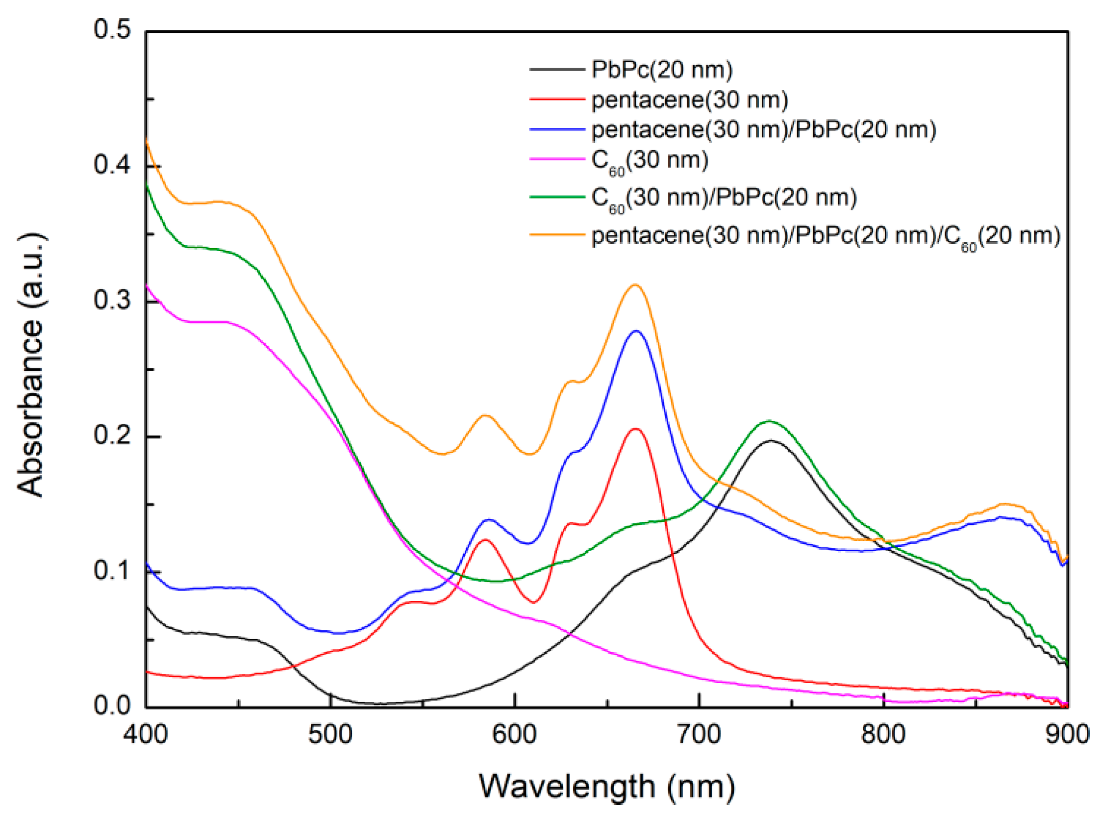
3. Results and Discussion

Quartz was used as the substrate for depositing the films. Figure 2 shows the absorption spectra of a variety of organic films. Examining the spectra reveals that the PbPc film displays strong NIR absorption due to π→π* electron transitions, whereas the pentacene film exhibits weaker absorption in the NIR region, and the C60 film shows no significant absorption in this wavelength range. The pentacene (30 nm)/PbPc (20 nm), C60(30 nm)/PbPc (20 nm), and pentacene (30 nm)/PbPc (20 nm)/C60(20 nm) films display desirable NIR absorption, which stems from the NIR absorption of PbPc film. It is observed that the NIR absorption of the pentacene/PbPc/C60, pentacene/PbPc, and C60/PbPc films is stronger than that of the PbPc film, and that of the pentacene/PbPc/C60, pentacene/PbPc films is higher than that of the C60/PbPc film. Generally, the evaporated PbPc film contains the monoclinic and triclinic phases, and the triclinic phase has higher NIR absorption than the monoclinic. Therefore, the higher the triclinic phase content in the PbPc film, the stronger the NIR absorption of the PbPc film, and thus, the more triclinic phase is expected to be produced in the evaporated PbPc film. In this place, the enhanced NIR absorption of the pentacene/PbPc/C60, pentacene/PbPc, and C60/PbPc films can be attributed to the increased triclinic phase content and crystallinity of PbPc films due to the template inducing of C60 or pentacene film, and pentacene has better template inducing for PbPc than C60, and thus the pentacene/PbPc/C60 and pentacene/PbPc films display stronger NIR absorption than C60/PbPc film. It is established that the high-mobility small-molecule materials have a good induction template to the low-mobility ones. The reason is that the high-mobility small-molecule materials always have a molecular orientation nearly perpendicular to the ab plane, and such a molecular orientation will produce a nice carrier transport in the ab plane, which is beneficial for field-effect transistors. Therefore, a better molecular orientation can be acquired in a low-mobility small-molecule material via template induction, leading to an enhancement in crystallinity, light absorption, etc.
In the evaluation of an OPT, there are two crucial parameters for assessing its photosensitive performance: photoresponsivity (R) and photo-to-dark current ratio (P). These parameters are defined as follows:
R = I p h / P o p t = | I i l l I d a r k | / P i n c A
P = I p h / | I d a r k |
where Iph = |IillIdark| is photocurrent, and Idark and Iill are the drain currents in the darkness and illumination, respectively. Where Popt stands for the optical power incident on the device channel, Pinc represents the power density of incident light, and A denotes the effective irradiated area. The detectivity (D*) signifies the minimum optical power required to generate photocurrent, while the external quantum efficiency (EQE) indicates the capacity to produce photo-generated carriers per individual incident photon. These parameters are defined as follows [28]:
D * = R A 1 / 2 ( 2 q I d a r k ) 1 / 2
where q = 1.6 × 10⁻¹⁹ C represents the elementary charge. And
E Q E = I p h / q P i n c λ / h c = R h c q λ
Here, h = 6.6 × 10⁻³⁴ J·s is Planck’s constant, λ is incident wavelength, and c = 3.0 × 10⁸ m/s is velocity of light.

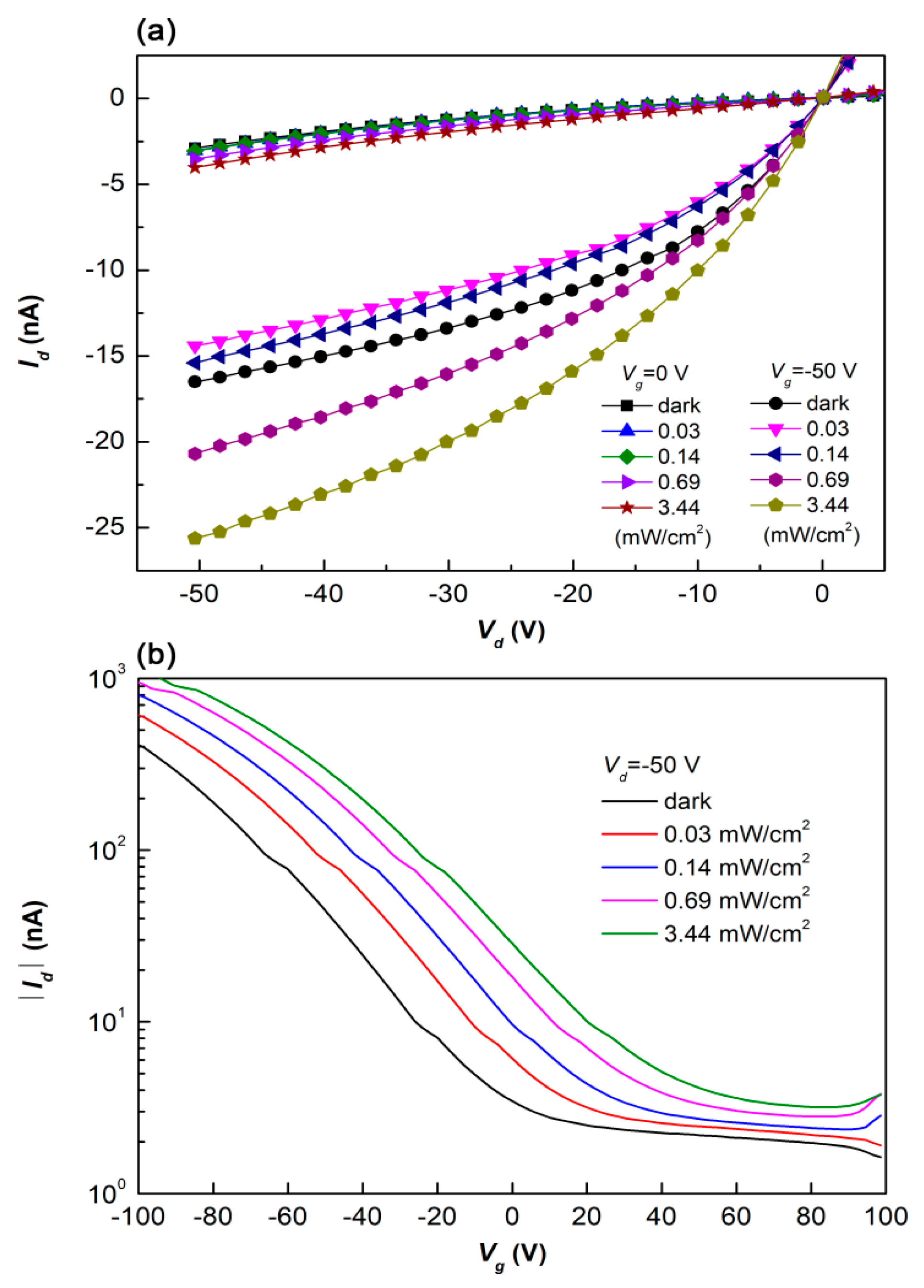
3.1. Single-Layer Devices

In Figure 3, we present the output and transfer characteristics of Dev-A under both dark and illuminated conditions. Notably, the PbPc single-layer OPTs display typical p-channel operation characteristics under negative gate voltage and drain voltage. Specifically, in the absence of light, the drain current (Id) at a drain voltage (Vd) of −50 V and gate voltage (Vg) of −50 V was measured to be merely −14.41 nA. Under illumination with an intensity of 3.44 mW/cm2, the drain current increases to −25.62 nA. The photocurrent (Iph) of the PbPc single-layer OPT is notably small, registering at 11.21 nA. Consequently, it exhibits a low R of 4.34 mA/W, a maximum photo-to-dark current ratio (Pmax) of 9.3, and an EQE of 0.65%. Due to its remarkably low carrier mobility of 8.5 × 10⁻⁴ cm2/V·s (as outlined in Table 1), Dev-A demonstrates suboptimal performance.

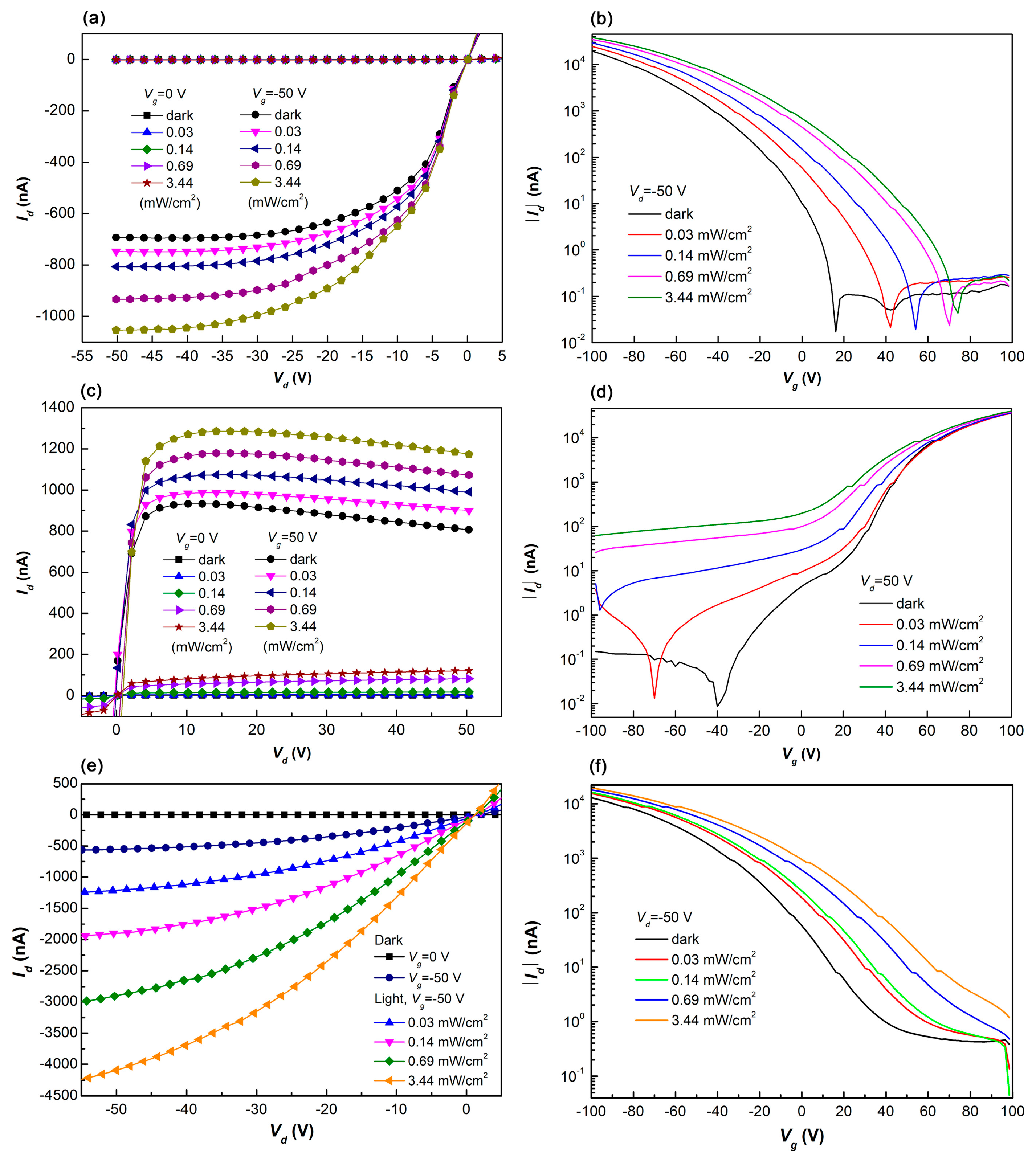
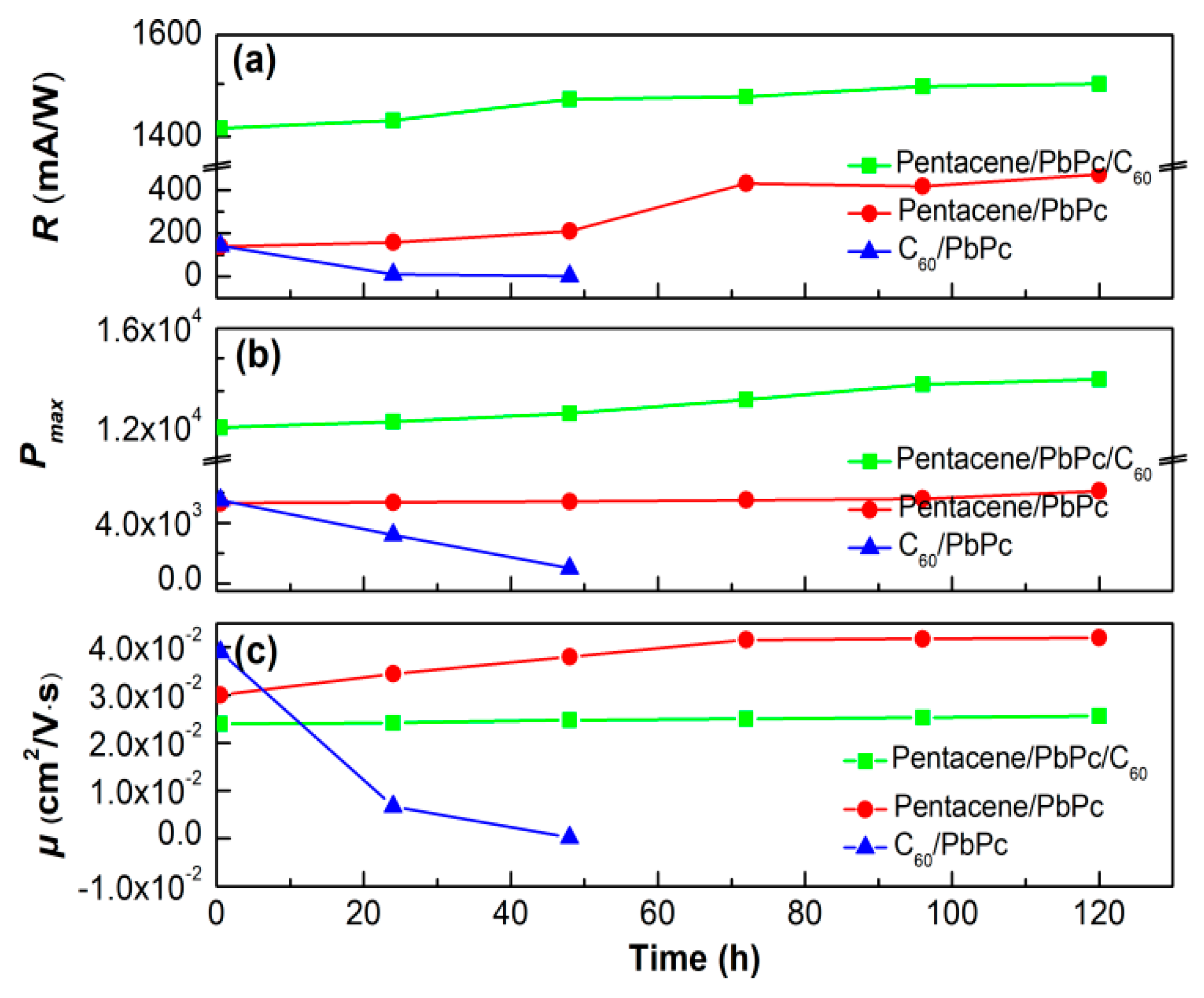
3.2. Bilayer Planar Heterojunction

Pentacene and C60 are typical hole and electron transport materials with high mobility [29,30]. To overcome the challenge of the low mobility of the PbPc film, a channel layer of either 30-nm-thick pentacene or C60 was introduced, and the PbPc film was used as the photoactive layer, that is, Dev-B and Dev-C. In Figure 4a,b, the output and transfer characteristics of Dev-B are presented, featuring the structure of Si/SiO2/pentacene (30 nm)/PbPc (20 nm)/Au. One can see that Dev-B has p-channel operation characteristics. In the dark, the Id of Dev-B at Vd = Vg = −50 V is −693.78 nA and rises to −1053.77 nA under 3.44 mW/cm2 illumination, and thus an Iph of 359.22 nA and an R of 139 mA/W are obtained, and the R of Dev-B is 32 times larger than that of Dev-A (Table 1). And at Vd = −50 V, a Pmax of 5.3 × 10³ of Dev-B is achieved, which is 570 times greater than that of Dev-A, and an EQE of 20.29% is acquired and bigger than that of Dev-A (see Table 1). The far superior performance of Dev-B to Dev-A is mainly ascribed to the higher NIR absorption and carrier mobility of Dev-B than Dev-A (see Figure 2 and Table 1), and the higher NIR absorption and carrier mobility of Dev-B benefit from the increased triclinic phase content and crystallinity of the PbPc films owing to template inducing of the pentacene layer [31]. In Figure 4c,d, we illustrate the output and transfer characteristics of Dev-C with a structure of Si/SiO2/C60 (30 nm)/PbPc (20 nm)/Au, which show that Dev-C has n-channel operation characteristics. In the dark, the Id of Dev-C at Vd = Vg = 50 V is 806.63 nA and increases to 1173.24 nA under 3.44 mW/cm2 illumination, and an Iph of 366.61 nA and R of 142 mA/W are gained, and the R of Dev-C is 33 times bigger than that of Dev-A (Table 1). And at Vd = 50 V, a Pmax of 5.5 × 10³ of Dev-C is obtained, which is 591 times larger than that of Dev-A, and an EQE of 20.73% is obtained and greater than that of Dev-A (see Table 1). Clearly, the performance of Dev-C is much better than that of Dev-A, which is largely due to the higher carrier mobility and exciton dissociation efficiency of Dev-C than Dev-A, and the higher exciton dissociation efficiency of Dev-C is a result of the newly established exciton dissociation centers at the C60 (acceptor)/PbPc (donor) interface. Due to relatively large energy barriers between the highest occupied molecular orbital (HOMO) levels and the lowest unoccupied molecular orbital levels of C60 and PbPc, a strong C60/PbPc interfacial electric field will be formed, and the excitons diffusing to the C60/PbPc interface will be dissociated into free electrons and holes. From the above, we can see that the performances of Dev-B and Dev-C are both far superior to those of Dev-A, reflecting the advantages of PHJ structure over a single layer.
Compared to Dev-C, Dev-B has equivalent mobility, higher NIR absorption, and lower exciton dissociation efficiency, which renders Dev-B to perform equivalently to Dev-C (shown in Table 1). The air stability of organic electronic devices has long been a concern. For this, the air stability of Dev-B and Dev-C was investigated. The R, Pmax, and mobility (μ) variations of them with storage time in air were plotted in Figure 5. It is clear that after 24 h, the R, Pmax, and μ of Dev-C plunge from 142 mA/W, 5.5 × 10³ and 3.9 × 102 cm2/V·s to 9.4 mA/W, 3.2 × 10³, and 6.7 × 103 cm2/V·s, respectively, while after 120 h, the R, Pmax, and μ of Dev-B rise from 139 mA/W, 5.3 × 10³, and 3 × 102 cm2/V·s to 473 mA/W, 6.1 × 10³, and 4.2 × 102 cm2/V·s, respectively. These results proved that Dev-B has far better air stability than Dev-C. The reason for this is that PbPc and pentacene are relatively stable for O2 and H2O in air, whereas C60 is highly sensitive to them [32,33,34,35,36]. When Dev-C exposes to air, the O2 and H2O molecules can permeate into the C60 layer and react with C60 to produce hydroxyls, and the hydroxyls would act as electron traps and capture lots of electrons [37], which causes a sharp decline in mobility and a serious deterioration of device performance (see Figure 5c). And when Dev-B is exposed to air, the O2 and H2O molecules are not easy to react with pentacene and PbPc, and thus Dev-B performs stably in air with time. Hence, given the performance and air stability of devices, the structure of Dev-B will be preferred.

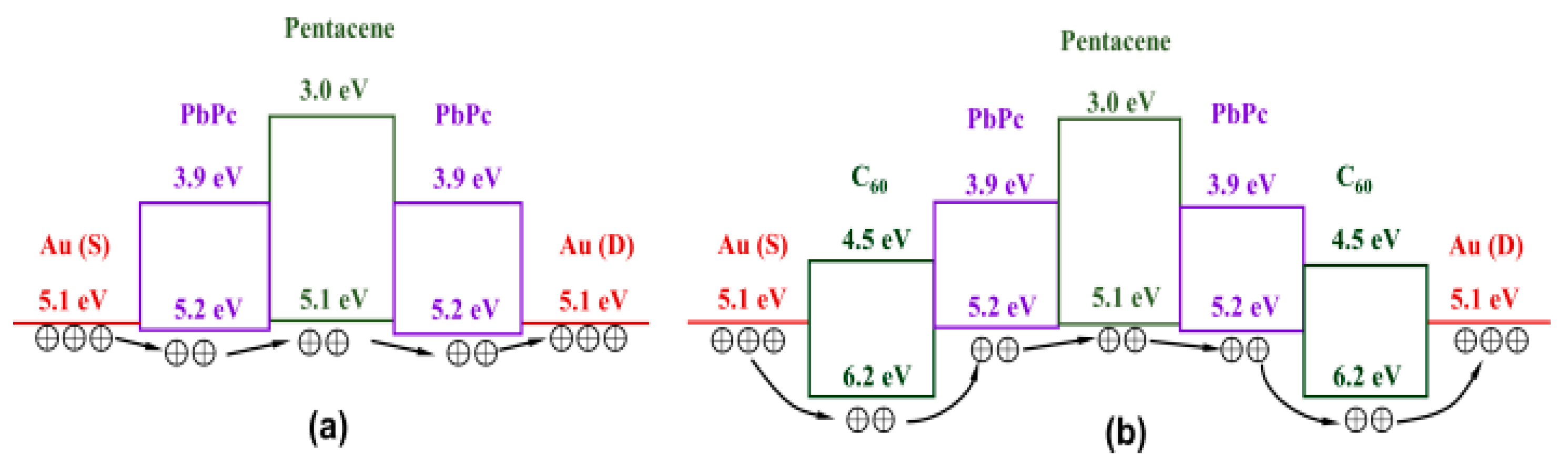
3.3. Tri-Layer Planar Heterojunction

The presence of dark current can significantly affect various aspects of a photodetector’s performance, including its photosensitive properties and power consumption. Therefore, in order to improve device performance and reduce power consumption, the dark current should be minimized in the design of the device.
In an effort to further diminish the dark current of Dev-B (Si/SiO2/pentacene (30 nm)/PbPc (20 nm)/Au), a C60 hole-blocking layer was deposited onto the surface of the PbPc/pentacene film. Consequently, an OPT (denoted as Dev-D) with the structure of Si/SiO2/pentacene (30 nm)/PbPc (20 nm)/C60 (20 nm)/Au was successfully fabricated. Figure 4e,f display the output and transfer characteristics of Dev-D. The most noticeable difference lies in the dark current, which has been significantly reduced to 81% (−562.41 nA) compared to that of Dev-B (−693.78 nA). At the same time, the photocurrent of Dev-D has increased by 1015% and reached 3651.24 nA. As can be seen from Table 1, the R of Dev-D rises to 1415 mA/W, which is 10 times bigger than that of Dev-B. The D* and EQE reach 7 × 10¹¹ Jones and 206.55%, which are 12 and 9 times larger than those of Dev-B, respectively. And it is noteworthy that the Pmax of Dev-D increases to 1.2 × 10⁴ substantially, surpassing that of Dev-B by 2.3 times. The decrease in dark current can primarily be attributed to the presence of the C60 acceptor layer, which can effectively block the holes from flowing towards the drain electrode. And the effective blocking is due to the relatively large energy barriers between the HOMO levels of PbPc and C60 and the HOMO level of C60 and the Fermi level of Au, as visually depicted in Figure 6. It can be seen that the energy barriers between the HOMO levels of PbPc and C60 and between the HOMO level of C60 and the Fermi level of Au are 1.0 eV and 1.1 eV, respectively, which are both much bigger than those of Dev-B (for Dev-B, the energy barriers between the HOMO levels of PbPc and pentacene and between the HOMO level of PbPc and the Fermi level of Au are 0.1 eV and 0.1 eV, respectively, as shown in Figure 6). In Dev-D, fewer holes can be injected into the C60 layer due to a big energy barrier lying between the HOMO level of C60 and the Fermi level of Au, and the holes injected into C60 layer may transport along the HOMO levels of active layer, and some of them might be blocked at the PbPc/C60 interface, and only the rest of them could be collected with the drain electrode successfully, thus generating a small drain current. Additionally, the μ of Dev-D is 2.4 × 10⁻² cm2/V·s, smaller than that of Dev-B (3.0 × 10⁻² cm2/V·s, shown in Table 1). This is also due to the presence of the C60 hole-blocking layer. Under the equal electric field effect, the hole drift velocity of C60 is far less than that of pentacene or PbPc. Therefore, the addition of the C60 layer gives rise to a decrement in both hole drift velocity and mobility. And the increase in photocurrent and photoresponsivity is thanks to the increased exciton dissociation efficiency owing to the newly established exciton dissociation centers located at the PbPc (donor)/C60 (acceptor) interface. Here, the excitons can be dissociated into free electrons and holes under an interfacial electric field. From the above, we can see that creating exciton dissociation centers in some ways is particularly beneficial for the performance of OPTs [28]. In summary, the overall performance of Dev-D, featuring a tri-layer PHJ structure, is better than that of Dev-A or Dev-B and surpasses that of the NIR OPTs reported in Refs. [26,27,31,38,39] (see Table 2).
The air stability of Dev-D was measured and shown in Figure 5. As can be seen, after 120 h, the R, Pmax, and μ of Dev-D increased from 1415 mA/W, 1.2 × 10⁴, and 2.4 × 102 cm2/V·s to 1500 mA/W, 1.38 × 10⁴, and 2.56 × 102 cm2/V·s by 6%, 15%, and 6.7%, respectively. The results indicated that Dev-D has superior air stability to Dev-B, and the air-sensitive C60 has almost no effect on the air stability of Dev-D. This is because the C60 layer located on the PbPc layer would play a key role in passivation and prevent O2 and H2O molecules from permeating towards PbPc to some extent. It is an interesting phenomenon that the device performance may deteriorate quickly when C60 acts as the channel layer in an OPT, whereas the device performance can be maintained well when C60 functions as the top-level passivation layer. This indicates that the air stability of the OPTs containing the C60 layer is linked to the position of the C60 layer. To sum up, C60 acts as a blocking layer, an exciton dissociation layer, and a passivation layer in Dev-D.

4. Conclusions

A series of NIR OPTs with distinct active layer configurations were manufactured. The absorption spectrum of the organic films and the electrical characteristics and air stability of the devices were measured. The results demonstrated that (i) the bilayer PHJ devices (Dev-B and Dev-C) have far superior photosensitive performance to the single layer ones (Dev-A) due to higher carrier mobility and light absorption of Dev-B and Dev-C than Dev-A; (ii) the bilayer PHJ ones with p-type channel (Dev-B) exhibit equivalent photosensitive properties to those with n-type channel (Dev-C) owing to stronger NIR absorption but lower exciton dissociation efficiency of Dev-B than Dev-C; (iii) Dev-B demonstrates much better air stability than Dev-C due to far superior stability of pentacene to C60 in air; (iv) the tri-layer PHJ ones (Dev-D) possess better photosensitive properties (R of 1415 mA/W and Pmax of 1.2 × 10⁴) than the bilayer PHJ ones with p-type channel (Dev-B), and the overall excellent photosensitive performance of Dev-D receives benefits from the merits of tri-layer PHJ structure including high light absorption, carrier mobility and exciton dissociation efficiency; and (v) the air stability of Dev-D is better than that of Dev-B; this can be ascribed to the passivation of the top-level C60 layer, and the C60 layer can effectively block O2 and H2O molecules from permeating into the PbPc layer.

Author Contributions

Conceptualization, Y.H., Y.L. and Y.W.; methodology, Y.H. and Y.L.; software, Y.H. and L.Z.; validation, Y.H., Y.L. and Y.W.; investigation, Y.H.; writing—original draft preparation, Y.H.; writing—review and editing, Y.H. and Y.L.; visualization, Y.H. and L.Z.; supervision, Y.W. All authors have read and agreed to the published version of the manuscript.

Funding

This research was funded by the development of high photoelectric conversion efficiency Si_PEDOT:PSS: PSS heterojunction solar cells, Youth Science Foundation of Lanzhou Jiaotong University, grant number 2021025.

Institutional Review Board Statement

Not applicable.

Informed Consent Statement

Not applicable.

Data Availability Statement

Data are contained within the article.

Conflicts of Interest

The authors declare no conflict of interest. The funders had no role in the design of the study; in the collection, analyses, or interpretation of data; in the writing of the manuscript; or in the decision to publish the results.

References

  1. Grassi, S.; Alamprese, C. Advances in NIR spectroscopy applied to process analytical technology in food industries. Curr. Opin. Food Sci. 2018, 22, 17–21. [Google Scholar] [CrossRef]
  2. Rathod, P.H.; Müller, I.; Van der Meer, F.D.; de Smeth, B. Analysis of visible and near infrared spectral reflectance for assessing metals in soil. Environ. Monit. Assess. 2016, 188, 558. [Google Scholar] [CrossRef]
  3. Sakudo, A. Near-infrared spectroscopy for medical applications: Current status and future perspectives. Clin. Chim. Acta 2016, 455, 181–188. [Google Scholar] [CrossRef] [PubMed]
  4. Zhang, Y.; Wang, Y.; Song, J.; Qu, J.; Li, B.; Zhu, W.; Wong, W.Y. Near-infrared emitting materials via harvesting triplet excitons: Molecular design, properties, and application in organic light emitting diodes. Adv. Opt. Mater. 2018, 6, 1800466. [Google Scholar] [CrossRef]
  5. Lee, D.; Han, S.Y.; Jeong, Y.; Nguyen, D.M.; Yoon, G.; Mun, J.; Chae, J.; Lee, J.H.; Ok, J.G.; Jung, G.Y.; et al. Polarization-sensitive tunable absorber in visible and near-infrared regimes. Sci. Rep. 2018, 8, 12393. [Google Scholar] [CrossRef]
  6. Wu, S.; Butt, H.J. Near-Infrared-Sensitive Materials Based on Upconverting Nanoparticles. Adv. Mater. 2015, 28, 1208–1226. [Google Scholar] [CrossRef] [PubMed]
  7. Hwang, D.K.; Lee, Y.T.; Lee, H.S.; Lee, Y.J.; Shokouh, S.H.; Kyhm, J.-H.; Lee, J.; Kim, H.H.; Yoo, T.-H.; Nam, S.H.; et al. Ultrasensitive PbS quantum-dot-sensitized InGaZnO hybrid photoinverter for near-infrared detection and imaging with high photogain. NPG Asia Mater. 2016, 8, e233. [Google Scholar] [CrossRef]
  8. Lei, Y.; Li, N.; Chan, W.-K.E.; Ong, B.S.; Zhu, F. Highly sensitive near infrared organic phototransistors based on conjugated polymer nanowire networks. Org. Electron. 2017, 48, 12–18. [Google Scholar] [CrossRef]
  9. Wu, G.; Fu, R.; Chen, J.; Yang, W.; Ren, J.; Guo, X.; Ni, Z.; Pi, X.; Li, C.Z.; Li, H.; et al. Perovskite/Organic Bulk-Heterojunction Integrated Ultrasensitive Broadband Photodetectors with High Near-Infrared External Quantum Efficiency over 70%. Small 2018, 14, 1802349. [Google Scholar] [CrossRef]
  10. Gasparini, N.; Gregori, A.; Salvador, M.; Biele, M.; Wadsworth, A.; Tedde, S.; Baran, D.; McCulloch, I.; Brabec, C.J. Visible and near-infrared imaging with nonfullerene-based photodetectors. Adv. Mater. Technol. 2018, 3, 1800104. [Google Scholar] [CrossRef]
  11. Wang, C.; Chen, X.; Chen, F.; Shao, J. Organic photodetectors based on copper phthalocyanine films prepared by a multiple drop casting method. Org. Electron. 2019, 66, 183–187. [Google Scholar] [CrossRef]
  12. Zheng, S.; Xiong, X.; Zheng, Z.; Xu, T.; Zhang, L.; Zhai, T.; Lu, X. Solution-grown large-area C60 single-crystal arrays as organic photodetectors. Carbon 2018, 126, 299–304. [Google Scholar] [CrossRef]
  13. Tong, S.; Yuan, J.; Zhang, C.; Wang, C.; Liu, B.; Shen, J.; Xia, H.; Zou, Y.; Xie, H.; Sun, J.; et al. Large-scale roll-to-roll printed, flexible and stable organic bulk heterojunction photodetector. NPJ Flex. Electron. 2018, 2, 7. [Google Scholar] [CrossRef]
  14. Su, Z.; Hou, F.; Wang, X.; Gao, Y.; Jin, F.; Zhang, G.; Li, Y.; Zhang, L.; Chu, B.; Li, W. High-Performance Organic Small-Molecule Panchromatic Photodetectors. ACS Appl. Mater. Interfaces 2015, 7, 2529–2534. [Google Scholar] [CrossRef]
  15. Luo, X.; Zhao, F.; Du, L.; Lv, W.; Xu, K.; Peng, Y.; Wang, Y.; Lu, F. Ultrasensitive flexible broadband photodetectors achieving pA scale dark current. NPJ Flex. Electron. 2017, 1, 6. [Google Scholar] [CrossRef]
  16. Urbani, M.; Ragoussi, M.-E.; Nazeeruddin, M.K.; Torres, T. Phthalocyanines for dye-sensitized solar cells. Coord. Chem. Rev. 2019, 381, 1–64. [Google Scholar] [CrossRef]
  17. Choi, M.-S.; Lee, S.; Kim, H.J.; Kim, J.-J. Inverted near-infrared organic photodetector with oriented lead (II) phthalocyanine molecules via substrate heating. Org. Electron. 2018, 61, 164–169. [Google Scholar] [CrossRef]
  18. Vijayan, L.; Thomas, A.; Kumar, K.S.; Jinesh, K. Low power organic field effect transistors with copper phthalocyanine as active layer. J. Sci. Adv. Mater. Devices 2018, 3, 348–352. [Google Scholar] [CrossRef]
  19. Hamam, K.J.; Alomari, M.I. A study of the optical band gap of zinc phthalocyanine nanoparticles using UV-Vis spectroscopy and DFT function. Appl. Nanosci. 2017, 7, 261–268. [Google Scholar] [CrossRef]
  20. Hamamoto, N.; Sonoda, H.; Sumimoto, M.; Hori, K.; Fujimoto, H. Theoretical study on crystal polymorphism and electronic structure of lead(ii) phthalocyanine using model dimers. RSC Adv. 2017, 7, 8646–8653. [Google Scholar] [CrossRef]
  21. Sekhosana, K.E.; Shumba, M.; Nyokong, T. Electrochemical and non-linear optical behavior of a new neodymium double-decker phthalocyanine. Polyhedron 2017, 138, 154–160. [Google Scholar] [CrossRef]
  22. Choi, M.-S.; Chae, S.; Kim, H.J.; Kim, J.-J. Control of Crystallinity in PbPc:C60 Blend Film and Application for Inverted Near-Infrared Organic Photodetector. ACS Appl. Mater. Interfaces 2018, 10, 25614–25620. [Google Scholar] [CrossRef] [PubMed]
  23. Chow, P.C.; Matsuhisa, N.; Zalar, P.; Koizumi, M.; Yokota, T.; Someya, T. Dual-gate organic phototransistor with high-gain and linear photoresponse. Nat. Commun. 2018, 9, 4546. [Google Scholar] [CrossRef]
  24. Binda, M.; Agostinelli, T.; Caironi, M.; Natali, D.; Sampietro, M.; Beverina, L.; Ruffo, R.; Silvestri, F. Fast and air stable near-infrared organic detector based on squaraine dyes. Org. Electron. 2009, 10, 1314–1319. [Google Scholar] [CrossRef]
  25. Song, X.; Zhang, Y.; Wang, R.; Cao, M.; Che, Y.; Wang, J.; Wang, H.; Jin, L.; Dai, H.; Ding, X.; et al. Bulk-and layer-heterojunction phototransistors based on poly [2-methoxy-5-(2′-ethylhexyloxy-p-phenylenevinylene)] and PbS quantum dot hybrids. Appl. Phys. Lett. 2015, 106, 253501. [Google Scholar] [CrossRef]
  26. Peng, Y.; Lv, W.; Yao, B.; Fan, G.; Chen, D.; Gao, P.; Zhou, M.; Wang, Y. High performance near infrared photosensitive organic field-effect transistors realized by an organic hybrid planar-bulk heterojunction. Org. Electron. 2013, 14, 1045–1051. [Google Scholar] [CrossRef]
  27. Li, Y.; Lv, W.; Luo, X.; Sun, L.; Zhou, M.; Zhang, J.; Zhao, F.; Zhong, J.; Peng, Y. Enhanced performance of isotype planar heterojunction photoresponsive organic field-effect transistors by using Ag source-drain electrodes. Europhys. Lett. 2015, 110, 17006. [Google Scholar] [CrossRef]
  28. Baeg, K.-J.; Binda, M.; Natali, D.; Caironi, M.; Noh, Y.-Y. Organic Light Detectors: Photodiodes and Phototransistors. Adv. Mater. 2013, 25, 4267–4295. [Google Scholar] [CrossRef]
  29. Yang, X.; Wang, G.; Liu, D.; Yao, Y.; Zhou, G.; Li, P.; Wu, B.; Rao, X.; Song, Q. Pentacene as a hole transport material for high performance planar perovskite solar cells. Curr. Appl. Phys. 2018, 18, 1095–1100. [Google Scholar] [CrossRef]
  30. Castro, E.; Fernandez-Delgado, O.; Arslan, F.; Zavala, G.; Yang, T.; Seetharaman, S.; D’Souza, F.; Echegoyen, L. New thiophene-based C60 fullerene derivatives as efficient electron transporting materials for perovskite solar cells. New J. Chem. 2018, 42, 14551–14558. [Google Scholar] [CrossRef]
  31. Li, Y.; Lv, W.; Luo, X.; Sun, L.; Zhao, F.; Zhang, J.; Zhong, J.; Huang, F.; Peng, Y. Enhanced performance of PbPc photosensitive organic field effect transistors by inserting different-thickness pentacene inducing layers. Org. Electron. 2015, 26, 186–190. [Google Scholar] [CrossRef]
  32. Collins, R.A.; Belghachi, A. Structural properties of lead phthalocyanine thin films. Mater. Lett. 1989, 8, 349–352. [Google Scholar] [CrossRef]
  33. Kumaki, D.; Yahiro, M.; Inoue, Y.; Tokito, S. Air stable, high performance pentacene thin-film transistor fabricated on SiO2 gate insulator treated with β-phenethyltrichlorosilane. Appl. Phys. Lett. 2007, 90, 133511. [Google Scholar] [CrossRef]
  34. Kagan, C.R.; Afzali, A.; Graham, T.O. Operational and environmental stability of pentacene thin-film transistors. Appl. Phys. Lett. 2005, 86, 193505. [Google Scholar] [CrossRef]
  35. Pevzner, B.; Hebard, A.F.; Dresselhaus, M.S. Role of molecular oxygen and other impurities in the electrical transportand dielectric properties of C60 films. Phys. Rev. B 1997, 55, 16439–16449. [Google Scholar] [CrossRef]
  36. Tsetseris, L.; Pantelides, S.T. Oxygen and water-related impurities in C60 crystals: A density-functional theory study. Phys. Rev. B 2010, 82, 045201. [Google Scholar] [CrossRef]
  37. Letizia, J.A.; Facchetti, A.; Stern, C.L.; Ratner, M.A.; Marks, T.J. High electron mobility in solution-cast and vapor-deposited phenacyl-quaterthiophene-based field-effect transistors: Toward n-type polythiophenes. J. Am. Chem. Soc. 2005, 127, 13476–13477. [Google Scholar] [CrossRef]
  38. Li, Y.; Pan, M.; Hu, Y.; Wang, Z.; Lv, W.; Peng, Y. The influence of substrate temperature on the near-infrared absorption and carrier mobility of lead phthalocyanine phototransistors. Thin Solid Films 2021, 718, 138481. [Google Scholar] [CrossRef]
  39. Huang, F.; Li, Y.; Xia, H.; Zhang, J.; Xu, K.; Peng, Y.; Liu, G. Towards high performance broad spectral response fullerene based photosensitive organic field-effect transistors with tricomponent bulk heterojunctions. Carbon 2017, 118, 666–674. [Google Scholar] [CrossRef]
Figure 1. Structure schematic diagrams of the NIR OPTs with different active layer structures. Devices (ad) correspond to Dev-A, Dev-B, Dev-C, and Dev-D, respectively.
Applsci 13 12613 g001
Figure 2. Photo-absorption spectra of PbPc, pentacene, pentacene/PbPc, C60, C60/PbPc, and pentacene/PbPc/C60 films.
Applsci 13 12613 g002
Figure 3. (a) Output and (b) transfer characteristics of the PbPc single-layer OPT (Dev-A) under both dark conditions and various incident light intensities.
Applsci 13 12613 g003
Figure 4. Output and transfer characteristics of Dev-B (a,b), Dev-C (c,d), and Dev-D (e,f) in the darkness and illumination.
Applsci 13 12613 g004
Figure 5. The R, Pmax, and μ variations of the PHJ devices with storage time in air. (a) R. (b) Pmax. (c) μ.
Applsci 13 12613 g005
Figure 6. Energy level diagram of (a) Dev-B and (b) Dev-D. Here, S and D are short for source and drain, respectively.
Applsci 13 12613 g006
Table 1. Device parameter summary from the experiments.
Active Layer Structuresμ a (cm2/V·s)R b (mA/W)PmaxD* (Jones)EQE
A: PbPc8.5 × 10−44.439.35.5 × 1090.65%
B: pentacene/PbPc3.0 × 10−21395.3 × 1036.2 × 101020.29%
C: C60/PbPc3.9 × 10−21425.5 × 1035.3 × 101020.73%
D: pentacene/PbPc/C602.4 × 10−214151.2 × 1047.0 × 1011206.55%
a Extracted from the following equation: Id = (W/2L)μCi(VgVth)2. b The obtained results were acquired under the incident light power condition of 3.44 mW/cm2 and Vd = −50 V.
Table 2. Comparison of device performance.
StructureResponse Wavelength
(nm)
R (mA/W) References
n+-Si/SiO2/CuPc/PbPc:PTCDA/Au808322 mA/W[26]
n+-Si/SiO2/PbPc/pentacene/Ag808123 mA/W[27]
n+-Si/SiO2/PbPc/pentacene(2 nm)/Au808505 mA/W[31]
n+-Si/SiO2/PbPc/Au85012.08 mA/W[38]
n+-Si/SiO2/C60/PbPc:AlClPc:PTCDA/Au850580 mA/W[39]
n+-Si/SiO2/pentacene/PbPc/C60/Au8501415 mA/Wthis work
Disclaimer/Publisher’s Note: The statements, opinions and data contained in all publications are solely those of the individual author(s) and contributor(s) and not of MDPI and/or the editor(s). MDPI and/or the editor(s) disclaim responsibility for any injury to people or property resulting from any ideas, methods, instructions or products referred to in the content.

