1. Introduction
The quad-flat no-lead package (QFN), as one of the primary packaging forms for integrated circuits, has gained widespread adoption in industrial applications due to its remarkable performance and cost advantages. Compared with the BGA package with the same I/O count, the QFN package not only features smaller dimensions and a lighter weight but also demonstrates superior thermal and electrical performance [
1]. These characteristics have facilitated extensive utilization of the QFN package in cutting-edge fields such as 5G. However, as the power of modern electronic products continues to increase, the heat generated by the QFN package has also risen progressively. Failure to effectively dissipate this heat may lead to product damage [
2,
3]. Therefore, in order to ensure the reliability of QFN products, a thorough analysis of their thermal performance is essential and of significant importance.
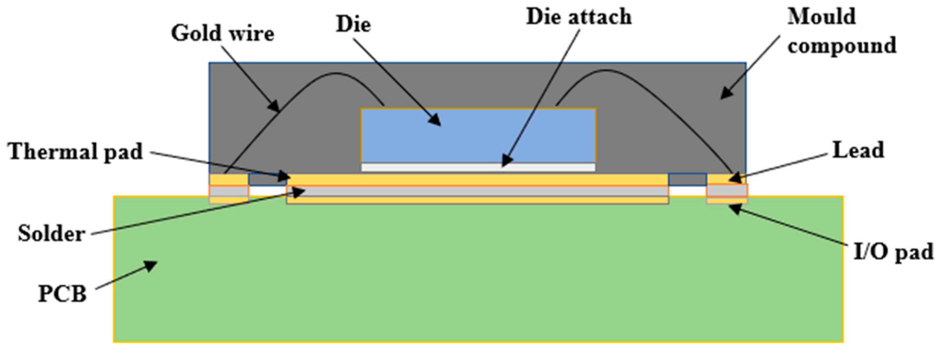
Most QFN packages are equipped with copper-based thermal pads on their undersides, which directly contact the silicon chip. The QFN package is soldered onto the copper-based thermal pad on the PCB. This design facilitates the efficient transfer of heat generated by the chip’s operation to the PCB, thereby reducing the internal temperature of the package.
The QFN package employs surface mount technology (SMT) for connection with PCB. The selected PCB material predominantly employs flame retardant (FR-4) for its cost-effectiveness and relatively minor environmental impact. However, the low thermal conductivity of FR-4 material results in elevated overall thermal resistance of the PCB, limiting heat conduction [
4]. To enhance thermal exchange between the PCB and its surroundings, a certain number of vias are typically designed beneath electronic components [
5].
Over the past decades, numerous scholars have conducted in-depth research on the thermal performance of QFN packages. At present, FEA has become the theoretical basis for engineering calculations and analysis. The finite element method can not only simplify complex problems but also save a lot of time and money. Krishnamoorthi [
6] designed a new type of QFN package with better thermal performance by using chip attachment film material attached to the chip. Chang [
7] predicted the effect of different convective conditions on the junction temperature of QFN packages using the finite element method. Fan [
8] introduced 3D simulations of multi-chip QFN systems for thermal analysis, employing CFD-based thermal modeling to predict heat behavior under temperature cycling. Suwa [
9] established a thermal resistance network between the chip and PCB through finite element modeling and associated simulations. Fu [
10] directly affixed carbon nanotubes as micro-scale heat sinks onto chips, significantly improving chip heat dissipation. Xia [
11] employed Flotherm computational fluid dynamics (CFD) software to predict the thermal performance of dual-row and conventional QFN packages. Bairi [
12] affirmed the positive effect of wire bonding technology on temperature regulation in QFN16b packages. Chen [
13] designed an integrated silicon-based microchannel heat dissipation module, shortening the heat conduction path and enhancing heat dissipation efficiency. Wang [
14] proposed a thermal resistance network analytical model for calculating the average chip temperature of QFN-packaged chips on PCB. Wang [
15] presented an enclosed cooling system integrating micro-pumps, heat exchangers, and silicon-based microchannel substrates to enhance cooling rates for high-power chips. Górecki [
16] used analytical equations to study the influence of metal lead length, the ambient temperature, the solder area, the power dissipated in the device, and heat sink size on the thermal resistance of the device, and the calculated and measured results are basically the same. Górecki [
17] also analyzed the effect of the choice of cooling system on the thermal parameters of thermally coupled power field effect tubes, and the results showed that the use of an active cooling system reduced the thermal resistance of the transistor under test by a factor of 20. Most of the more established methods of heat dissipation today involve adding a heat sink to the component. The heat sink can improve heat dissipation by increasing thermal convection. We intend to improve the heat dissipation of components by improving the heat conduction process.
It has been demonstrated that PCBs with thermal vias can significantly reduce thermal resistance during heat conduction [
18]. Li [
19] designed a congestion-minimizing hot-channel planning algorithm, which proved to be very effective in directly eliminating local hot spots. Beng [
20] investigated the effect of different numbers of heat vias on the thermal resistance improvement of PCBs. Gautam [
21] investigated the heat dissipation effect of four thermal via designs for power devices. Hossain [
22] used carbon nanotubes (CNT) instead of copper as vertical heat sinks in a 3D chip and investigated its heat dissipation potential through finite element analysis. Simulation results show that carbon nanotube vias have better heat dissipation performance in 3D chips compared to conventional copper vias. Li [
23] predicted solder joint thermal reliability through studying PCB pad design layouts for multi-row QFN packages. Shen [
24] analyzed the effect of different design parameters on the thermal resistance of the through-hole and proposed an optimal design trajectory to minimize the thermal resistance of the through-hole. Wilcoxon [
25] measured gaps within the thermal pad of various solder alloy compositions and microvia configurations in test boards, indicating that vias might introduce gaps without compromising the reliability or thermal resistance of QFN. Hollstein [
26] used finite element analysis to show that increasing PCB thickness and bottom thermal pad thickness can enhance the heat dissipation capacity of QFN packages. Górecki [
27] studied PCB thermal resistance influenced by designing PCBs with nine different thermal via layouts, and the results showed that it was possible to reduce the thermal resistance value by 34% just by changing the layout of the PCB. Currently, most of the research objects for thermal vias are traditional packages, which are not fully adaptable to various kinds of packages. Moreover, the design of thermal vias is mostly limited to the thermal pad, which does not fully utilize the excellent heat dissipation performance of thermal vias.
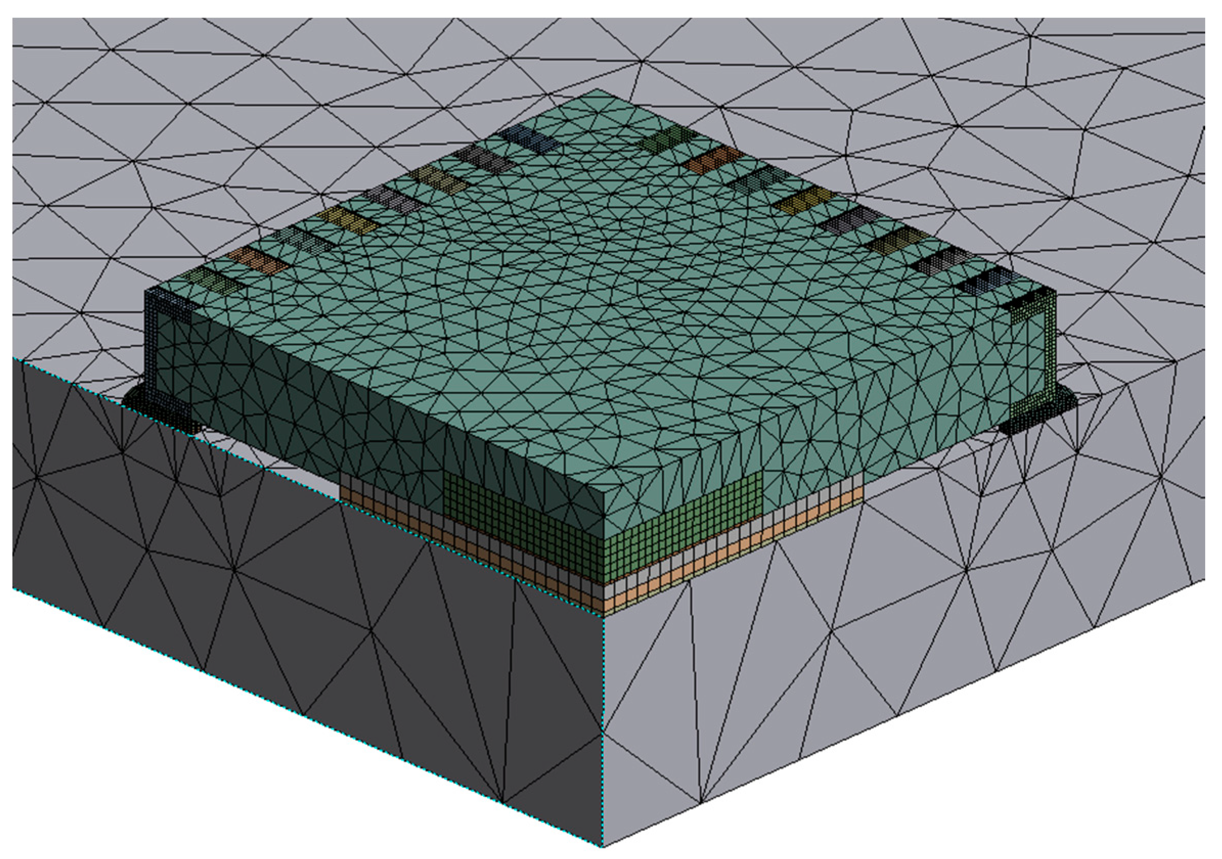
This study aims to conduct three-dimensional simulation analysis on QFN packages soldered onto PCB, with a focus on exploring the impact of thermal vias on the heat dissipation characteristics of high-lead QFN packages, followed by comparative analyses with conventional QFN and dual-row QFN. Firstly, reference parameters for the dimensions and material properties of the three QFN packages are provided, and model construction is achieved. In this paper, the influence of thermal via placement on the heat dissipation process of the high-lead QFN package is analyzed. It then describes two types of thermal via distribution (square and circular) located below the thermal pads and compares their heat dissipation effects. Subsequently, conventional QFN, dual-row QFN, and high-lead QFN packages are presented around the thermal vias placed around the I/O pads to illustrate the relationship between the maximum temperature of the three QFN packages and the diameter of thermal vias, as well as the thickness of copper plating.
3. Simulation Results
In this paper, we have primarily embraced fundamental steady-state thermal analysis and static structural analysis methodologies to comprehensively assess the heat dissipation capabilities and thermal stress characteristics of the QFN package. Our analytical framework begins by elucidating the simulated outcomes pertaining to the high-lead QFN package under varied thermal via parameters. Subsequently, building upon this foundation, we undertake an in-depth exploration encompassing the conventional QFN, dual-row QFN, and high-lead QFN packages, with the overarching objective of pinpointing the QFN package that exhibits optimal thermal performance alongside its corresponding optimal thermal via parameters.
3.1. Steady-State Analysis of High-Lead QFN Package under Reference Conditions
To ascertain the temperature distribution, we have employed convective boundary conditions. Our assumption is that the model operates under natural convection conditions, with a convection coefficient set at 20.0 W/(m² °C). The internal heat generation rate of the QFN component during operational states is considered to be 0.1 W/mm
3. The power dissipation of the device is about 0.24 W. Furthermore, radiation effects have been disregarded. Under these established conditions, the calculated temperature distribution is depicted in
Figure 4a. The observations reveal a notably uniform temperature distribution around the high-lead QFN package, signifying the transfer of heat from the die to the PCB, subsequently diffusing further across the PCB. Through computation, it is evident that the maximum temperature is concentrated around the chip, reaching a peak value of 58.4 °C.
In the context of static structural analysis, we have imposed displacement constraints in the X, Y, and Z directions at the bottom of the PCB board. Additionally, symmetric constraints have been enforced on the vertical planes in the X and Z directions to restrain displacements beyond the plane and rotations within the plane. By employing the outcomes of the fundamental steady-state thermal analysis, we have fed inputs into the static structural analysis module, rendering the stress distribution depicted in
Figure 4b. The calculated outcomes underscore the occurrence of the maximum stress at the junction of the solder joint and the I/O pads, with a peak stress value of 386.3 MPa.
In order to further validate the excellent thermal performance of the high-lead QFN package, we used two additional QFN packages (the conventional QFN package and the dual-row QFN package) as references.
Figure 5 illustrates the temperature distribution of these two QFN packages under reference conditions. The maximum temperature of the conventional QFN package is 58.6 °C. Compared to the high-lead QFN package, the heat dissipation of the conventional QFN package is poor. While the maximum temperature of the dual-row QFN package is 58.8 °C. The heat dissipation in the dual-row QFN package is the worst among the three packages.
3.2. Effect of Distance of Thermal via to the Center on Heat Dissipation of High-Lead QFN Package
Due to the relatively low thermal conductivity of the PCB, the heat generated by the die often accumulates between the die and the PCB, leading to an elevation in temperature. In order to address this concern, this section investigates the impact of thermal vias on the thermal dissipation performance of the high-lead QFN package by introducing thermal vias into the PCB. We explore this issue by analyzing the influence of thermal vias at different positions on the temperature distribution and conducting a comprehensive comparison against the results under baseline conditions. To mitigate the influence of multiple thermal vias, we have limited the number of thermal vias to one (
Figure 6). Simultaneously, we have controlled the diameter and the copper plating thickness of the thermal vias. In this section, the diameter of the thermal via is set at 0.3 mm, with a copper plating thickness of 0.02 mm, ensuring a fair comparison between thermal vias positioned at various locations.
Figure 7 illustrates the maximum temperature scenarios for the high-lead QFN package at different distances from the thermal via to the center of the heat source. It is observable that as the thermal via distance increases, the maximum temperature progressively rises. When the thermal via is located in the central position, the maximum temperature of the high-lead QFN package is 57.4 °C, indicating optimal heat dissipation performance. Compared to the baseline scenario, the maximum temperature has been reduced by approximately 1.0 °C. This observation indicates that the closer the thermal via is to the heat source, the more pronounced its effect on the thermal dissipation of the high-lead QFN package. It is worth noting that the high-lead QFN package shows a significant temperature change occurring within the range of 2 mm to 2.5 mm for thermal via distances. This is attributed to the thermal via positioned at 2 mm, located beneath the thermal pad and solder joint, facilitating efficient heat transfer and consequently better heat dissipation. Conversely, the heat generated by the die is not effectively transferred to the thermal via positioned at 2.5 mm, resulting in inferior heat dissipation performance.
3.3. Effect of Different Thermal via Distributions on Heat Dissipation in High-Lead QFN Packages
Based on the discussion in the previous section, we can deduce that the closer the thermal vias are to the heat source, the more pronounced their effect on the thermal dissipation of the high-lead QFN package. In order to deeply study the heat dissipation effects of thermal vias, this section explores two distinct thermal via distribution patterns: square distribution and circular distribution (
Figure 8). Our focus will be on investigating the impact of thermal via quantity under these two distribution conditions on heat dissipation performance. Concurrently, we have controlled the diameter and the copper plating thickness of the thermal vias at 0.3 mm and 0.02 mm, respectively.
Figure 9 presents the maximum temperatures for the high-lead QFN package under square distribution and circular distribution conditions with different numbers of thermal vias. The computational outcomes reveal that as the number of thermal vias increases, their contribution to heat dissipation becomes progressively more substantial. Notably, when the thermal via quantity reaches 9, the maximum temperature of the high-lead QFN package with thermal vias that are circularly distributed is 56.1 °C, which is slightly better than that of the square-distributed thermal vias. However, with a further increase in the number of thermal vias, the square distribution of these thermal vias demonstrates a remarkable enhancement in heat dissipation effectiveness. Beyond 13 thermal vias, the heat dissipation performance of the square distribution becomes even more significant. This observation can be attributed to the fact that with a higher number of thermal vias, the circular distribution results in a more closely packed arrangement, causing heat accumulation and hindering timely heat conduction. When the number of thermal vias is 25, the maximum temperature of the high-lead QFN package with square-distributed thermal vias is 54.2 °C, which is 1.8 °C lower relative to that for thermal vias of 9.
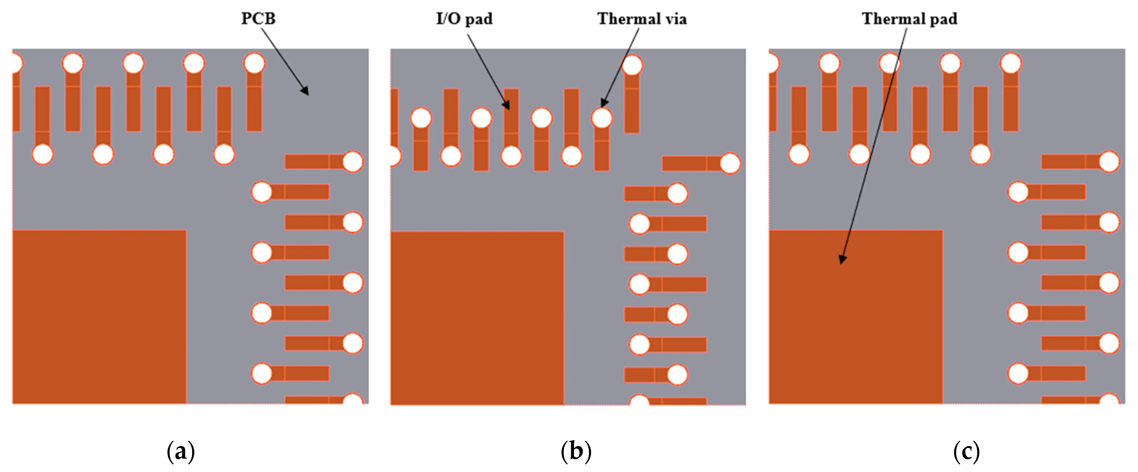
3.4. Integration of Thermal Vias with I/O Pads on PCB
While introducing thermal vias around the thermal pads can enhance the heat dissipation performance of the QFN package, the efficiency of heat transfer from the die to these thermal vias is relatively lower, resulting in suboptimal heat dissipation. To further optimize the heat dissipation efficiency, we consider the placement of thermal vias around the I/O pads and integrate these thermal vias with the I/O pads (
Figure 10). To ensure simulation accuracy, the distance between the thermal vias and the I/O pads is set at 0.3 mm.
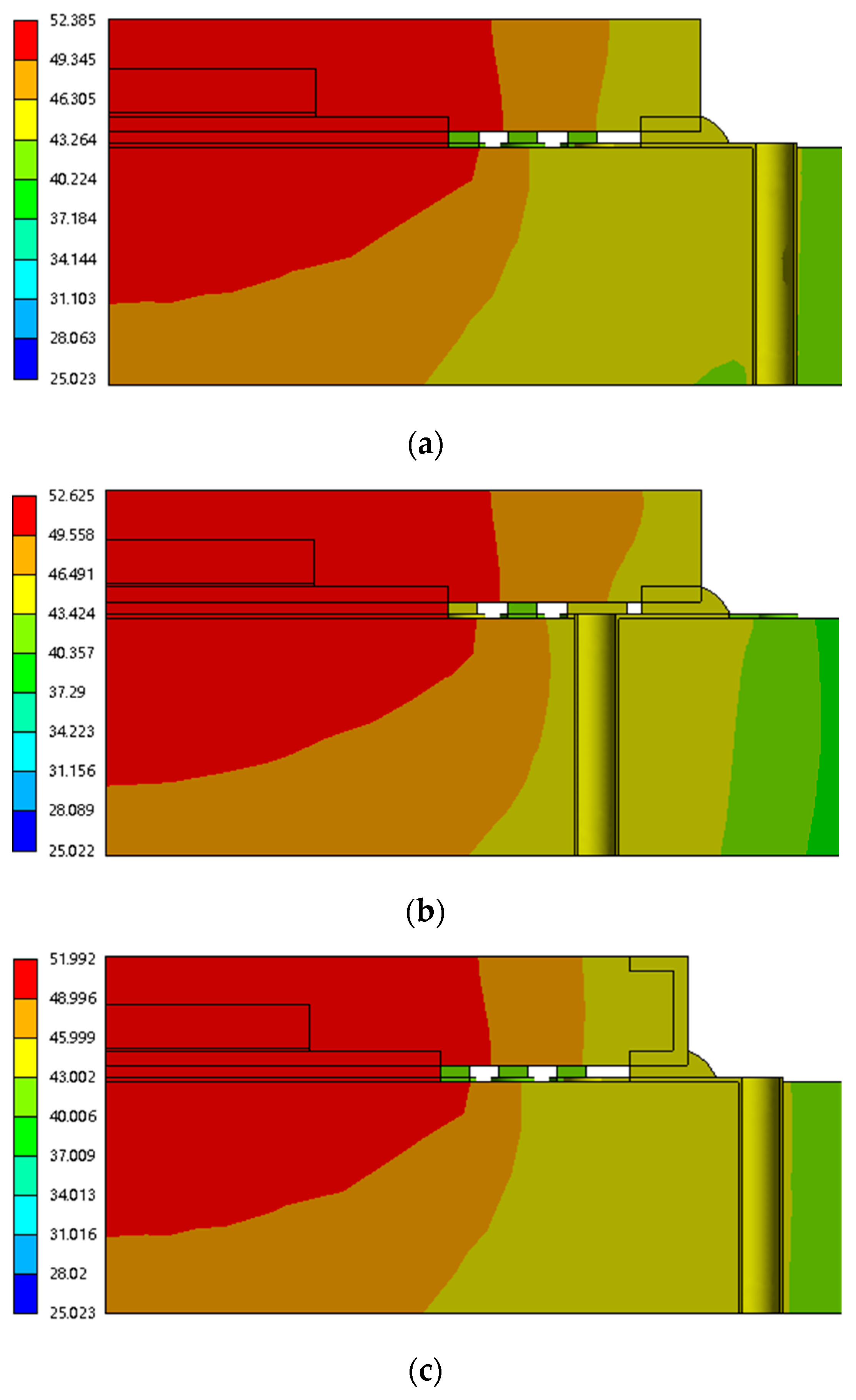
Figure 11 shows the temperature distribution of three different types of QFN packages under these conditions. The maximum temperatures of the conventional QFN, the dual-row QFN, and the high-lead QFN packages are 52.4 °C, 52.6 °C, and 52.0 °C, respectively. It is evident that among these three QFN packages, the high-lead QFN package demonstrates the best heat dissipation performance when thermal vias are combined with the I/O pads, resulting in a reduction of 6.4 °C in the maximum temperature. Therefore, this approach significantly enhances the heat dissipation efficiency of the QFN package. Furthermore, this method also substantially lowers the temperature of the solder joints, thereby reducing solder joint thermal stress and improving the solder joint’s operational lifespan.
To further validate the excellent thermal performance of high-lead QFN, the variation of the maximum temperature of the three QFN packages with different thermal via diameters and copper plating thicknesses was discussed. Firstly, with the copper plating thickness of 0.02 mm, the effects of thermal via diameters ranging from 0.2 mm to 0.5 mm on chip heat dissipation were investigated. Subsequently, keeping the thermal via diameter at 0.3 mm, the copper plating thickness was gradually increased from an initial value of 0.01 mm to a maximum of 0.15 mm, ensuring that the vias were fully filled with copper.
Figure 12 illustrates the variation of the maximum temperature under different thermal via diameters. It is observed that with an increase in thermal via diameter, the maximum temperature decreases gradually for all three QFN packages, concurrently reducing thermal stress. The maximum temperature of the conventional QFN package has decreased from 53.5 °C to 50.6 °C. For the dual-row QFN package, the maximum temperature has decreased from 53.883 °C to 50.614 °C. The high-lead QFN package has seen a reduction in its maximum temperature from 53.1 °C to 50.2 °C. This is attributed to the larger thermal via diameter, which increases the contact area between heat and air, thus enhancing heat convection. Notably, the high-lead QFN package consistently maintains the lowest maximum temperature.
Figure 13 presents the variation of the maximum temperature under different copper plating thickness conditions. The results indicate a general increase in the maximum temperature for all three QFN packages as the copper plating thickness increases. The maximum temperature of the conventional QFN package increased from 52.4 °C to 54.9 °C. The maximum temperature of the dual-row QFN package increased from 52.6 °C to 55.5 °C. The maximum temperature of the high-lead QFN package increased from 52.0 °C to 54.5 °C. This rise is attributed to the increased copper thickness elongating the heat transfer path, subsequently elevating thermal resistance and affecting the heat dissipation effectiveness of the thermal vias. The increase in coper plating thickness from 0.01 mm to 0.02 mm resulted in a relatively small increase in the maximum temperature for all three QFN packages. This phenomenon is attributed to the reduced heat capacity of the copper plating layer when the thickness of the copper plating is decreased. Even in these scenarios, the high-lead QFN package maintains the lowest maximum temperature.
Based on the data presented in this section, it can be concluded that, under variations in thermal via diameter and copper plating thickness, the high-lead QFN package exhibits superior heat dissipation performance.
4. Conclusions
The study employs finite element analysis to investigate the impact of thermal via design on the heat dissipation performance of high-lead QFN packages in comparison with conventional QFN and dual-row QFN packages. A systematic examination of four factors—thermal via distance, quantity, diameter, and copper plating thickness—was conducted, employing fundamental steady-state thermal analysis and static structural analysis techniques. Corresponding models were established using Ansys software, yielding a series of valuable outcomes.
In this paper, we verify the effectiveness of thermal vias and the superiority of heat dissipation in high-lead QFN packages. The analysis results indicate that, within the high-lead QFN package, a closer proximity of thermal vias to the heat source corresponds to more significant heat dissipation effects. Thermal vias situated beneath the thermal pad exhibit enhanced heat dissipation effectiveness. When designing thermal vias, we should try to arrange the thermal vias as close as possible to the heat source and try to ensure complete contact between the thermal vias and the heat source. Increasing the quantity of thermal vias enhances heat dissipation, with square distribution layouts showing more distinct advantages over circular ones, particularly when the quantity of thermal vias is substantial. When components that require heat dissipation are soldered to the PCB, we should maximize the number of thermal vias and arrange them in a square distribution.
We verified the effectiveness of combining I/O pads and thermal vias. This design not only reduces the junction temperature of the QFN packages but also significantly lowers the temperature of the solder joints, thus reducing the thermal stress at the solder joints. In cases where solder joints are prone to failure due to high temperatures, we can use this design to improve the solder joint life. Enlarging the thermal via diameter contributes to improved heat dissipation. However, elevating the copper plating thickness may amplify the PCB’s thermal resistance, exerting adverse effects on QFN heat dissipation. In general, under consistent conditions of thermal via diameter and copper plating thickness, the high-lead QFN package demonstrates optimal heat dissipation performance. All of these conclusions are based on a model with uniform thickness, homogeneous structure, and perfect contact between the materials.
In summary, this study provides a solid theoretical foundation and practical guidance for designing new QFN packages and optimizing PCB structures. This study helps to improve the heat dissipation performance of QFN packages for manufacturing more reliable electronic components. The investigations were performed for the PCB containing only one copper layer. The thermal vias could be more important when the PCB with two copper layers is used. In our future work, we will continue to improve the heat dissipation of QFN packages through the combined optimization of the heat convection process and the heat conduction process. In future work, we will design experiments to verify the obtained computation results.


