Abstract
This paper presents several conclusions based on time domain analysis of the simulation results of several transmission lines that use frequency-dependent dielectrics, highlighting the fiberglass effect on performance. The matching conditions of the circuit are checked based on a Smith chart simulation that represents the magnitude of the reflection coefficient via scattering parameters. A time domain analysis is provided by means of the eye diagram, which allows the study of the rise and fall time, jitter, and eye height and width of the two materials considered to be appropriate for the examination of composite substrates: one conventional substrate, FR4, and one more oriented to high-speed design constraints, N4000-13. Time domain analyses highlight the effect of increasing the rate for our purpose on the composite substrate for coupled or single-ended interconnections or routes on PCBs.
1. Introduction
The necessity of high-speed paths puts distinctive constraints on dielectrics, with a smaller dielectric constant, Dk, due to the inverse proportionality between the velocity and the square root of the dielectric constant. One main issue is the costs of the overall system, which will rise due to substrate cost; thus, using the N4000-13 substrate with low loss at higher frequencies, given by the loss tangent of the dielectric, Df, is more costly in comparison to a common substrate like FR4. The cost of the design will also increase because a good estimation of the electromagnetic and signal integrity is needed. All new IoT applications, 5G networks, and high-speed circuits need low latency and low jitter even for high data rates; thus, timing analysis is necessary while minimizing power consumption.
High-speed circuits impose constraints on PCB substrates with lower dielectric constants, where lower permittivity allows higher velocity and, thus, maximum data rates. However, this can significantly increase system costs, as both analog and digital applications require PCB material selection based on dielectric properties. Common dielectric materials like FR4 exhibit reduced performance and significant frequency-related issues.
This paper is an extension of [1] written as a partial result of the research carried out by the same group of authors, where several primary results were obtained and presented, while in this work, the topic has been expanded by conducting a new series of simulations and measurements and extracting several interesting conclusions based on the larger set of results. Since it proves that the subject is of interest, we consider that its development is valuable. While in [1], we highlighted the presence of FWE only through the study of insertion and reflection parameters; here, we aim to demonstrate the presence of FWE through time domain analyses using eye diagrams.
In [2], the authors presented a new delay deviation measure to quantify the delay in single-ended links, and they evaluated the differential skew exceedance to estimate the unpredictability in differential links. Those measured were calculated by various simulations and several interesting results were highlighted. It is important to say that the development of the study depends on the trace width and separation.
In [3], specimens of varying thicknesses were tested at different stress levels, and various analyses, including acoustic emission, infrared thermography, and micro-CT, were conducted. The study also observed thermoelastic effects, crack diversion, and delamination at elevated stress levels, with thicker specimens showing increased crack growth and susceptibility to manufacturing defects. Numerical and experimental results indicated that specimen thickness influences crack growth patterns.
The authors of [4] explored the impact of fiber hybridization on the tensile fracture of 3D woven textile composites. It was the first investigation of its kind in this context. The hybridization led to increased modulus with higher carbon fiber volume fractions but a proportional decrease in strength (78% of the baseline glass). Fiberglass can still maintain 80% of its original strength, a significant improvement over nonhybrid materials with no hybridization. Cases showed a residual strength higher than the initial strength, like the thick unsymmetrical and functionally graded in the warp direction. In general, the warp direction retained a residual strength comparable to the weft. Unsymmetric samples displayed coupled behavior, influenced by thermally induced shrinkage. These findings highlight the tradeoff involved in hybridization methods.
In [5], the authors investigated the impact of fabric areal weight on the mechanical properties of carbon-fiber-reinforced polymer composite laminates. Three different twill weaves with areal weights of 380, 630, and 800 g/m2 were used to create laminates. The research showed that decreasing fabric areal weight leads to significant increases in tensile strength, elastic modulus, and in-plane shear stress, offering valuable insights for material selection in industrial applications and enhancing the understanding of composite behavior.
The impact of various weave structures on fabric comfort and mechanical properties of fiber-reinforced composites was presented in [6]. Fabrics using different materials in the warp and weft directions, with four weave types each, were examined. Hybrid fabrics with specific weaves demonstrated superior air permeability, moisture management, and thermal resistance. In composites, different weaves exhibited enhanced mechanical properties, suggesting applications in window coverings, sports equipment, and, potentially, the automotive industry.
The authors of [7] evaluated different propagation of acoustic signals with different CFRPs, and several material proprieties were also researched. Fiber orientation, ply number, and material geometry proved to have an important role because they affect the acoustic wave during propagation; with that in mind, the negative side effects are loss of peak amplitude, duration, and energy of the recorded signals.
In [8], the author proposed a new structure that modeled the FWE and cross-talk phenomena for high data rate differential lines designed in PCB. It was shown that the substrate of composite is essential in the construction aspect for such lines, and it was concluded that frequency-dependent materials framework needs to be implemented and FWE must be pre-evaluated in the design chapter. The time domain and frequency domain indicate the priority of accurate model use for intersymbol interference prevention, which is a crucial aspect in signal quality evaluation.
The authors of [9] explained the benefit of using Modal Acoustic Emission (MAE) on Composite Overwrapped Pressure Vessels (COPV). The paper examined this path, which is an encouraging method that brings more data to typical acoustic emission techniques. It also discusses how MAE signals are used for mode extraction from AE signals. As a conclusion, it demonstrated that extensional and flexural modes were splatted, and their frequency bandwidths were described. With all of this in mind, MAE is encouraging but demands more examination.
In [10], the authors raised issues regarding the connection between Acoustic Emitted (AE) signal features and Fiber–Resin Composite Materials (FRCM) that may damage the transmitted signal because of fiber weaving. It was shown that the axial fibers layer is the main bearer of the signal, while the interweave oblique fiber can shift the values of the amplitude, number of received sounds, and their energy and duration. They concluded that AE proved to be a good solution for testing the FCRM with sophisticated fiber waving.
The authors of [11] applied the AE technique to check glass/epoxy laminated when exposed to mode II delamination loading conditions. A Hilbert Transform (HT) signal processing approach was used and the results concluded that this approach was relevant to measure damage mechanisms and better compliance was settled. In addition, the HT boosted signal characterization.
In [12,13], the authors presented several results related to the effects of surface treatment, creation process, and architecture on the mechanical and environmental setting of laminated jute/epoxy campsites. It was shown that the use of unidirectional fabric architecture raised the strength and tensile modulus. Also, the paper showed that jute/epoxy laminar composites have almost the same stiffness-to-mass ratio as glass fabric/epoxy laminar composites.
In [14], the authors evaluated the delamination propagation in glass/epoxy composites under mode I quasi-static and fatigue loading conditions. Several connections were made between the AE energy and the free strain energy. In a third-degree polynomial, connections between the cumulative AE energy of delamination and cumulative crack growth were anticipated with the AE method. The advantage of the AE method is in predicting delamination rise using one sensor without the demand to estimate AE propagation velocity. This approach is a tough technique for detecting and analyzing the crack length.
In [15], the authors presented the negative contribution of a few factors (in terms of skew, losses, dispersion, etc.) that can alter the high-speed design performance. The fiber weave effect is statistical in essence and it is challenging to regulate the timing skew, which is defined as the time difference in the arrival of the signal on a differential pair of routes at the end of it. This evaluation does not mean that, inevitably, a deviation of the skew budget will necessarily cause the system to crush, but the authors concluded that more elaborate modeling and simulation of the channel was needed, as well as compensation of the FWE at the receiver end. In [16], the author described and compared the signal transmission on interconnections with various specifications of the fiber weave, finding various approaches to enhance the FWE effect so that high-speed digital developers have a complete evaluation of it. The author concluded that, for high data rates, better results are obtained by using flattened fiber weaves (such as 1078 and 1035) and NE-glass fiber weaves (such as 2116NE). Also, ref. [11] suggested using long signal lines parallel to the weft direction or rotating the image with a proper angle. If the fiber weave pitch is not known, an angle of 5 degrees should be considered for proper routing and skewing conditions. The authors of [17] presented the results regarding FWE on PCB substrates and the inflicting problems of high-speed and high-frequency signal integrity on different electronic devices. Better outcomes can be observed when using a 3D printer for high-performance Additively Manufactured Electronics (AME) devices; therefore, the DragonFly LDM is recommended for developing AME. In [18], the authors proposed several ways to improve and avoid issues with resonances and insertion loss dips, by accounting for the skew and ensuring the calculated impedance demand and the precise average dielectric constant for utilization in impedance estimations. In [19,20,21], the authors explored the result of using PCB weave on signal integrity in terms of mode transformation and differential channel loss to intra-pair skew. The researchers used Keysight ADS 2DEM transformations to explore the scattering parameters and eye diagram for signal broadcasting at 1 Gbps and 10 Gbps. They concluded that NE-glass fiber with thick weave such as 3313 should be used in PCB substrate to decrease the attenuation and intra-pair skew. The loss due to fiber weave outcome should be kept below 5%, as additional channel loss impacted by different factors like dielectric loss and cooper surface harshness should be also considered. Using the K supercomputer, examiners have identified a new state of graphene that is being investigated for all kinds of applications.
In [22], an assessment was conducted on circuits designed using both microstrip and stripline technologies, calculating the time delay difference between them. The study revealed the detrimental impact of FWE on circuit performance. For better performance, it is recommended to use a denser fabric and a new technique for better spreading out the glass cloth. The authors developed a solution to mitigate the impact of the anisotropic dielectric properties of PCBs. A model was designed in HFSS and signal integrity analysis was executed using IBIS-AMI models in ADS with equalization techniques applied at the receiver. A dielectric material with very good qualities can deliver better performance to the whole system, but the fact needs to be considered that with lower Df there is lower Dk, but the cost of the given substrate increases. In [23], the authors aimed to soften the skew contributed by woven glass of PCB dielectrics, by using a combination of low Dk spread glass, laminated with multiple ply glass. Dielectrics are made up of molecules and atoms; thus, the effect of an applied electromagnetic field cannot move at macroscopic distances. Evaluation has found that the applied electric field can shift the orientation of the interrelated charges inside the material [24,25].
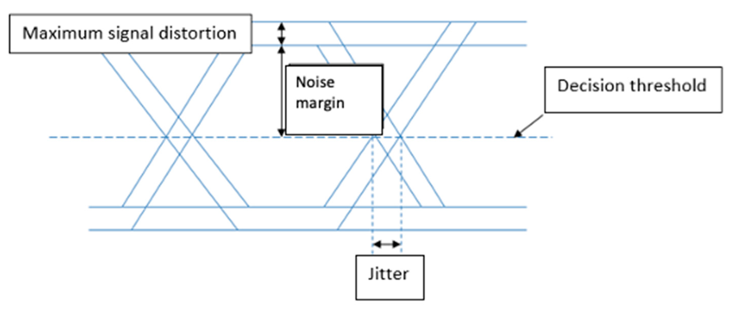
The eye diagram is an illustration of overlays of thousands or millions of bits corresponding to the transmitted signal. The arrangement of bits 0 and 1 can influence the integrity of the signal propagation if collective transitions from 0 to 1 or 1 to 0 happen in a tight period. The purpose of eye diagram representation is to describe the propagation over a given channel, for a given rate of the source signal and special parameters: levels of 0/1 s, eye opening or height and width of the eye, eye amplitude, bit rate, transitions, rising and falling edges, and jitter. Those are the major high-speed signal parameters in signal examination that may display channel imperfections [26,27]. Some of these parameters are illustrated in Figure 1.
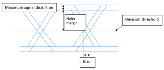
Figure 1.
Eye diagram—general representation and main parameters.
Levels 0/1, also named logical levels, represent the amplitude corresponding to these levels. The eye opening should be equivalent to the amplitude of the propagated signal, but in practice, the noise can also change the amplitude. Rise and fall times matter the most for calculating the middle values of the signal thresholds from 0 to 1 and vice versa. Jitter is the deflection of signal propagation times between the two levels [28,29,30].
To have a physical dielectric model, the frequency behavior needs to be known, thus, transmission models with frequency-dependent parameters are necessary [31,32,33,34,35].
In this paper, the main contribution is the study of the time and frequency domains of two materials, FRR4 and N4000-13. The simulations are carried out in two design technologies (microstrip and stripline) for different values of the frequency. Secondly, for a more detailed study, we will evaluate several parameters that help us highlight the better behavior of the N4000-13 material compared to the common FR4 material. The parameters to be studied are the rise and fall times, the transition from high level to low level, and the jitter and amplitude values of the eye mask.
The subject of this research is focused on high- and very high-frequency circuit design and analyses, as shown within the references cited by this work. From those references, we may highlight [2] where a well-known tool in the circuit design industry is used, particularly in the field of simulations and analyses of paths for high- and very high-frequency signals. Simbeor (version 2023.01—beta), a software recognized worldwide in the Printed Circuit Board (PCB) design, was developed for precise simulations of signal behavior in such environments.
The purpose of our article is to demonstrate the importance of determining the occurrence of jitter in high-speed circuits and reducing it to increase the system performance.
The novelty of this work lies in:
- Highlighting the fiberglass effect on the system performances using eye diagrams;
- Checking the matching conditions via scattering parameters using Smith charts;
- Designing circuits, simulations, extracting data, and interpreting the results in this software, MWO (Microwave Office, version V22.1) from AWR DE, which is a work-oriented program for high-frequency applications; however, it is not specific for modeling certain materials, and accomplishes this behavior by implementing the equations for the substrates used in the design tool.
The main contribution consists of the:
- Implementation of the circuits in the MWO design tool from AWR-DE;
- Selection of the parameters of the specifications for two substrates, a low-cost, conventional FR4 and a high-speed-oriented substrate, N4000-13, from the data sheets;
- Implementation and analysis of the circuits;
- Extraction of data from these simulations, their analysis, and the interpretation of results.
2. Problem Statement and Issues
A transmission line is a structure consisting of two or more conductors that connect to a signal generator and along which an electromagnetic wave propagates. For this study, we will consider the model in which two parallel conductors, which are separated by a layer of dielectric material, are used to interconnect a transmitter with a receiver. Their role is to ensure the transmission of undistorted information between the system components.
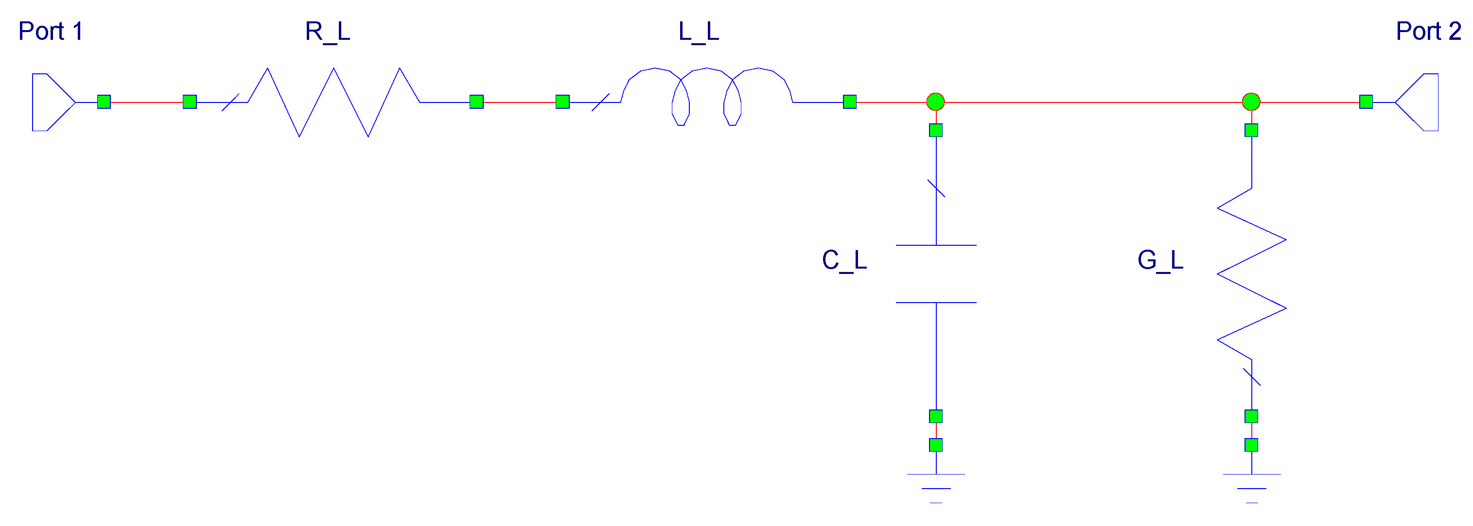
Next, the transmission line structure using per-unit-length parameters is presented in Figure 2.
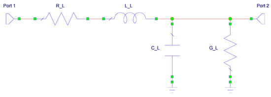
Figure 2.
Transmission line with per-unit-length parameters.
Figure 2.
Transmission line with per-unit-length parameters.
- -
- [Ω/𝑚] is the line resistance (total resistance per unit length of the two conductors) and represents the losses in the conductor that increase with the frequency;
- -
- [𝐻/𝑚] is the line inductance (inductance of the two-conductor system per unit length of the line);
- -
- [𝐹/𝑚] is the line capacitance (insulator capacitance between line conductors per unit length);
- -
- [𝑆/𝑚] is the line conductance (the conductance of the two-conductor system per unit length of the line) and represents the losses in the dielectric that increase with the frequency.
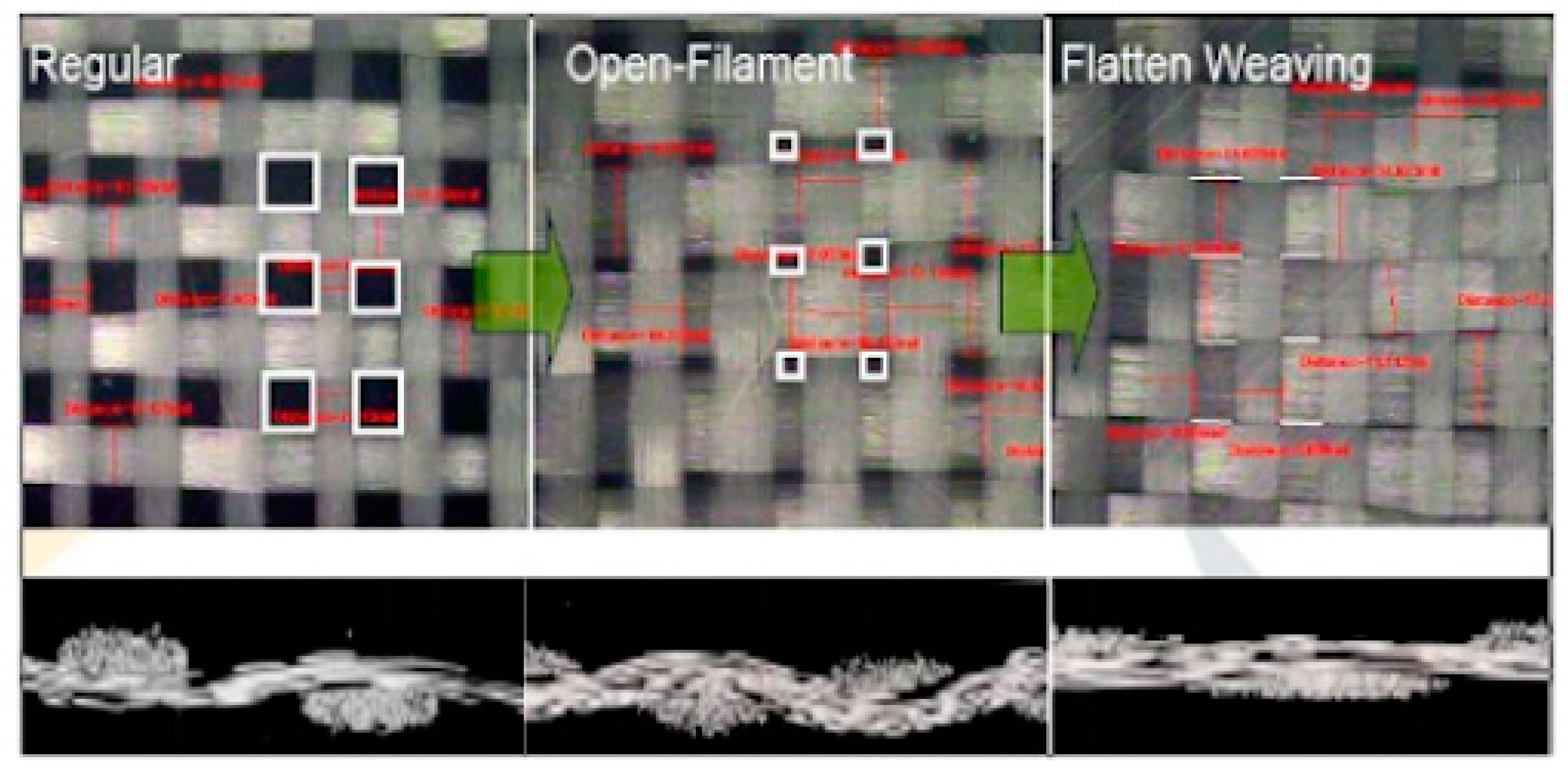
FWE hinders circuit performance, particularly at speeds exceeding 3 Gbps, due to variations in the dielectric constant. This leads to differential distortion in signal lines, increasing bit error rates, especially for long high-speed transmissions. As speed, distance, and discontinuities rise, significant signal losses occur. This signal loss due to dielectric loss at higher frequencies is observed in [26]. As transmission speeds increase, multiple factors affect signal integrity. Figure 3 shows varying fiber optic styles, from loose to tight waves.

Figure 3.
Fiber weave styles. Loose weaves (left) create greater skew and impedance variations in a board compared to a tight weave (right) [15].
An efficient evaluation of the signal integrity can be performed based on an examination of circuit performances at different frequencies, which can be achieved based on the evaluation of the scattering parameters and by time analysis of the eye diagram.
For short distances and low data rates, signals travel reliably from transmitter to receiver. However, longer distances and higher speeds lead to significant signal degradation. Signal integrity assesses the quality of electric signals during transmission. PCB design depends on substrate characteristics, and a key limitation is the non-uniform distribution of resin and fibers in the substrate material. When using composite materials with an inhomogeneous structure and equal-length differential lines, differences in signal propagation times create skew. This skew results in signal asymmetry, potentially shifting from differential to common mode, leading to eye diagram closure, jitter, and distortions in rise and fall times. This phenomenon is known as the Fiber Weave Effect (FWE) [23].
The difference between the propagation times of the two differential signals can be determined using the relationship [24]:
where:
- -
- is the difference between the propagation times;
- -
- is the length of the transmission line or of the coupled lines in the case of differential lines;
- -
- is the relative permittivity of the dielectric;
- -
- is the speed of light ( 𝑚/𝑠).
Relation (1) can also be written as:
where:
- -
- is the maximum relative permittivity of the dielectric;
- -
- is the minimum relative permittivity of the dielectric;
- -
- is the length of the transmission line or the coupled lines in the case of differential lines;
- -
- is the speed of light ( 𝑚/𝑠).
To be able to evaluate the losses in a circuit, we need the distribution parameters, also known as the S parameters. There are two types of S parameters: are parameters that characterize the reflection coefficient and are parameters that characterize the transfer coefficient.
The insertion loss for interconnections, denoted by IL, represents the loss of power due to the transmission line, which is seen as a transmission channel with losses expressed for the dielectric and conductor and is related to the reflection coefficient [12] by:
For maximum signal transmission, we must have insertion losses close to 0 dB.
If the system impedance does not match the terminal impedance, then the signal is reflected at the input terminal. The input reflection loss, denoted by RL, is the reflection coefficient of the signal at the input gate and is similarly expressed in dB.
In general, to ensure a maximum transfer of power from source to destination, the reflection losses at the input gate should be as small as possible; in a standard communication system, an acceptable value for RL should be below −30 dB.
The purpose of our paper is to highlight the presence of the fiber tissue effect through graphic representations in the time domain. We will extract data from time domain representations and draw conclusions about rise times, fall times, and jitter.
In [2], the authors presented different patterns for very high-speed buses designed in Double Data Rate (DDR) technologies—DDR5 operates at 8.4 GT/s and DDR6 works at 12.8 GT/s—and analyzed them in terms of delay and impedance variations, comparing different patterns of fiber weaves as 1030, 1080, 1078, and 3313 in terms of delay deviation exceedance and differential skew exceedance. Similar interconnection types are analyzed; single-ended and differential PCB interconnect as they are analyzed in our systems. The main point of interest here is the variation of skew, but this should be completed with information regarding jitter, eye corners figures in different substrates, microstrip, and stripline. The results can be easily extracted from the eye diagrams, making data rate and substrate type swappable, as will be demonstrated in Chapter 3. The same 10 GHz data rate was of interest in [2] and the S parameters were indicated to be represented with the frequency variation to extract information about the periodic response in terms of the reflection coefficient. Additionally, in [1], it was demonstrated that insertion loss should be analyzed to highlight the influence of the attenuation over a certain length with the increase of frequency.
In [15], the authors turned their attention to the fiber weave effect only for high-speed PCBs, and compared different fiber wave patterns, such as 1035, 1078, 1080, and 2166, in terms of impedance fluctuations and phase difference on the traces at high data rates, over 56 Gbps. The dielectric constant fluctuation of different types of fiber weaves was analyzed for the mentioned patterns, affecting the impedance of the trace and signal propagation delay. In this research, the focus was oriented towards impedance fluctuation in time and phase difference in frequency, for rates up to 4 Gbps. Here, the study would also be complete if additional information regarding jitter was provided.
To perform the simulations, we used the MWO environment from AWR [34]. Using this program, we designed circuits with two coupled and uncoupled lines in microstrip and stripline technologies for two materials, FR4 [35] and N4000-13 [36], and, using them, we performed simulations to obtain the eye diagram and the Smith chart and evaluated the performance of the designed circuits.
2.1. Implementation of Circuits with Two Coupled Lines
In this subchapter, we will present the model and the results obtained based on the simulation of a two-coupled line implemented in microstrip and stripline technologies, using FR4 and N4000-13 as s. Figure 4 presents the model of the coupled lines implemented, made in microstrip technology and FR4 substrate. The dielectric constant and loss tangent of the dielectric for the composite substrate FR4 are and

Figure 4.
FR4 substrate microstrip technology coupled lines.
To obtain proper matching conditions at the ports, we determined the even and odd mode impedances and, based on these, we obtained the values of common and differential mode impedances, as presented in [1].
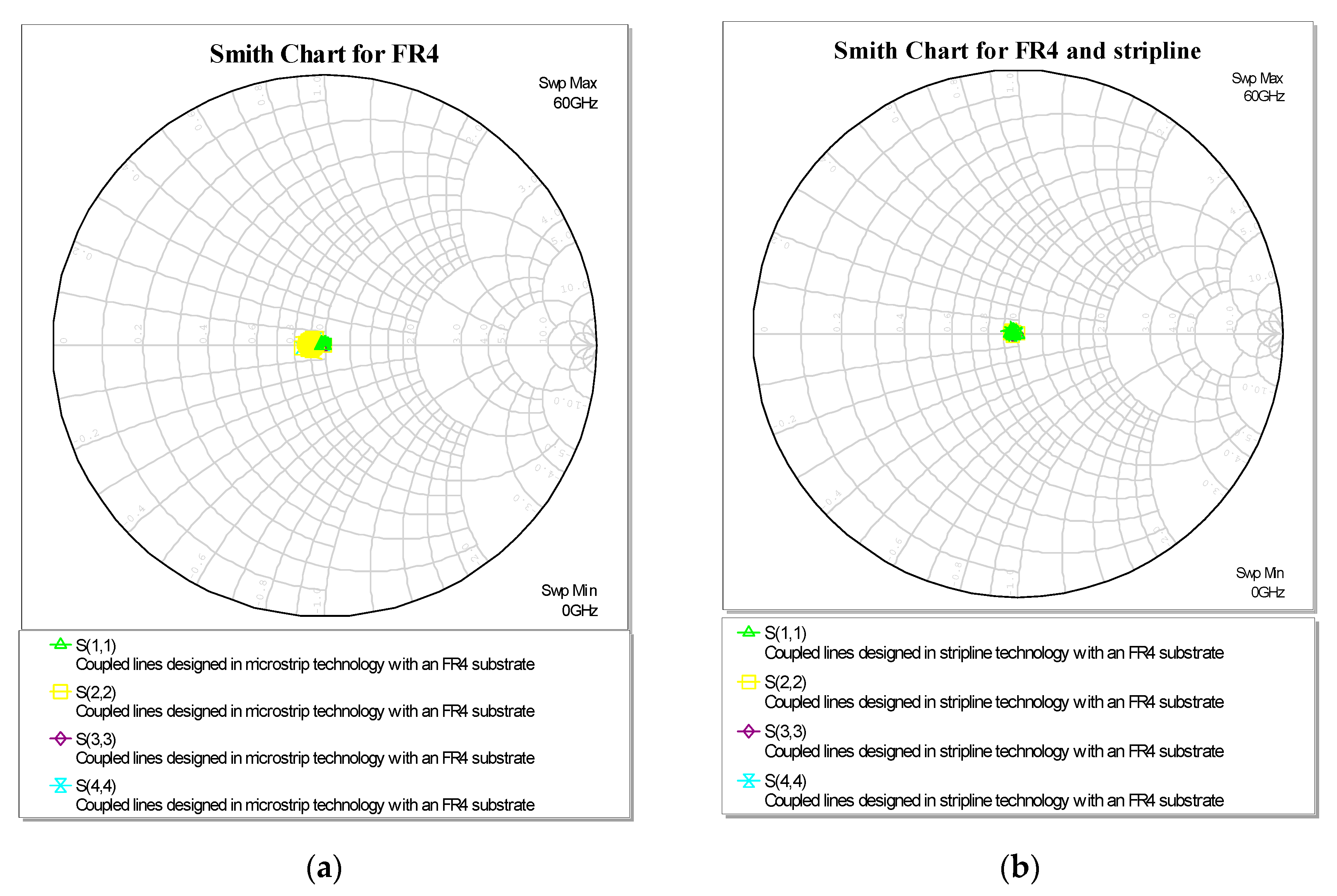
Using the Smith charts, presented in Figure 5a (for microstrip technology) and Figure 5b (for stripline technology), we checked if the circuits were matched by representing the reflection parameters. Matching is obtained when the parameters are in the middle of the Smith diagram, as shown in Figure 5, corresponding to progressive waves at the ports.
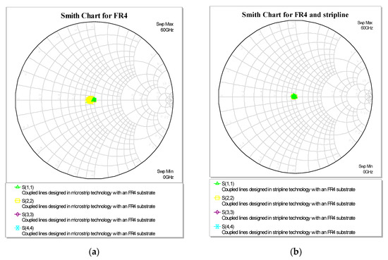
Figure 5.
(a). Plotting the parameters on the Smith chart after matching the circuit containing two coupled microstrip lines on a uniform FR4 substrate. (b) Plotting the parameters on the Smith chart after matching the circuit containing two coupled striplines on a uniform FR4 substrate.
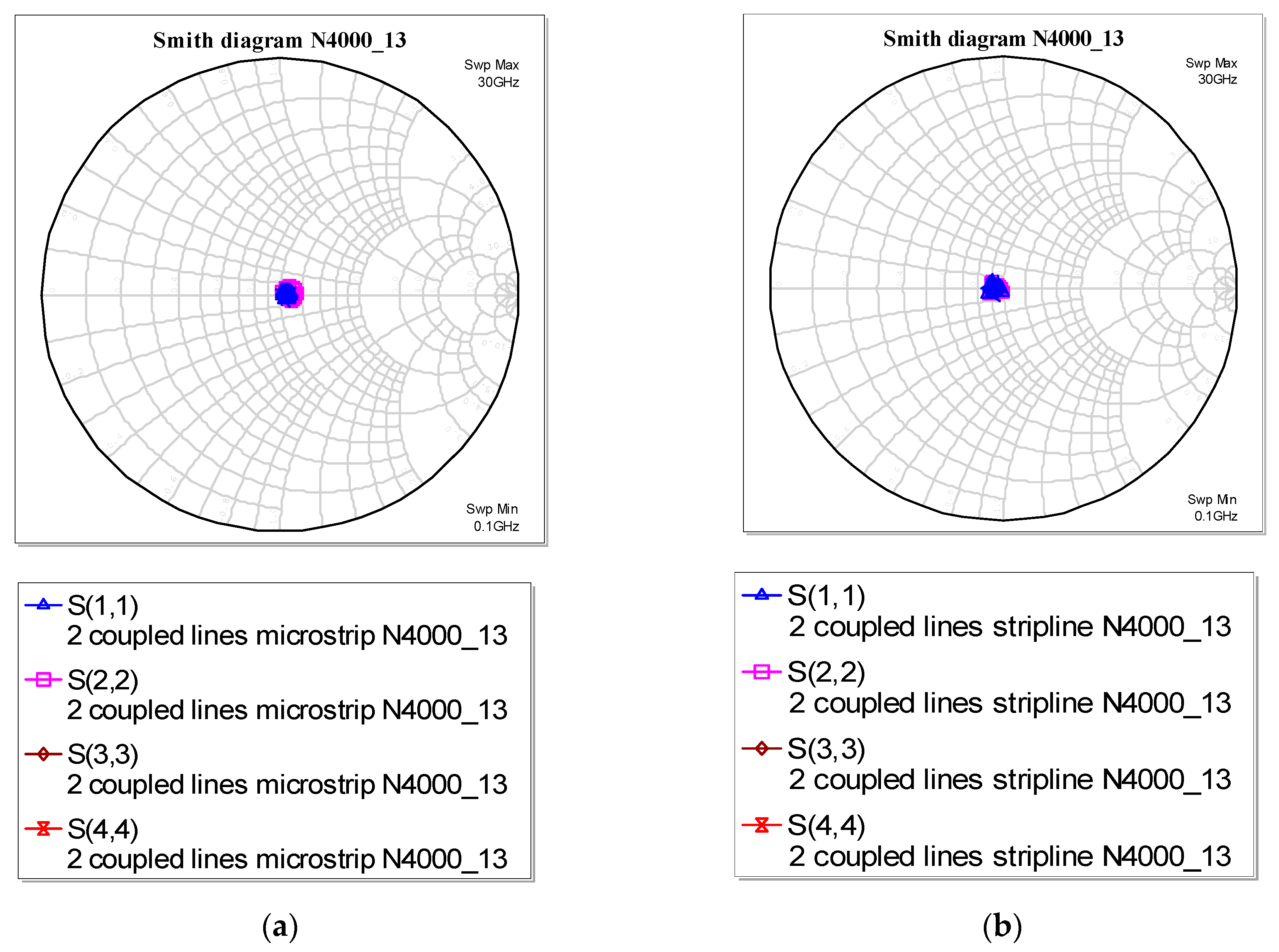
Next, we implemented the same circuit and simulations for the second material. We noticed that, in Figure 6, in this case, the values for the common and differential impedances were different; thus, based on the Smith chart evaluation of the reflection coefficients, we observed that the circuit is not matched at the ports. Therefore, we optimized the values of these impedances so that the circuits were matched, as can be seen in Figure 7.
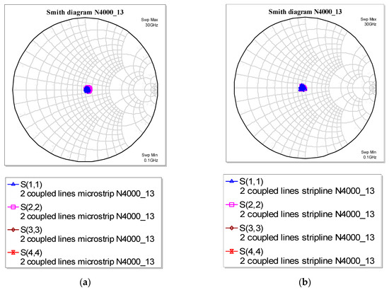
Figure 6.
(a). Plotting the parameters on the Smith chart after matching the circuit containing two coupled microstrip lines on a uniform N4000-13 substrate. (b) Plotting the parameters on the Smith chart after matching the circuit containing two coupled striplines on a uniform N4000-13 substrate.

Figure 7.
FR4 substrate microstrip coupled lines with a pseudo-random source.
To verify the performance of the circuit, an analysis in the time domain is performed. To do this, a pseudo-random signal source is connected at the input port, both for the circuit designed in microstrip technology and the one designed in stripline technology. Figure 8 represents a circuit implemented in microstrip technology with an FR4 substrate and pseudo-random signal source at port 1. This is a pseudo-random bit sequence with a parametrized rate, number of symbols and samples per symbol, rise and fall times, and window type. To highlight the effect of increased rate, the parameter RATE is varied between 1 and 30 GHz and the influence of sharp edges of the signals and transitions are specified by TR and TF rise and fall time. These are important for critical applications and the results are also influenced by the window type selection. TR and TF are set to 10 ps.
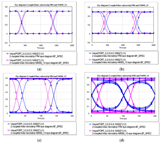
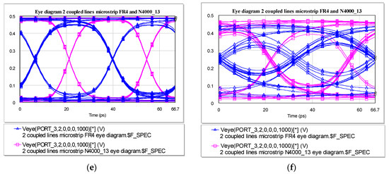
Figure 8.
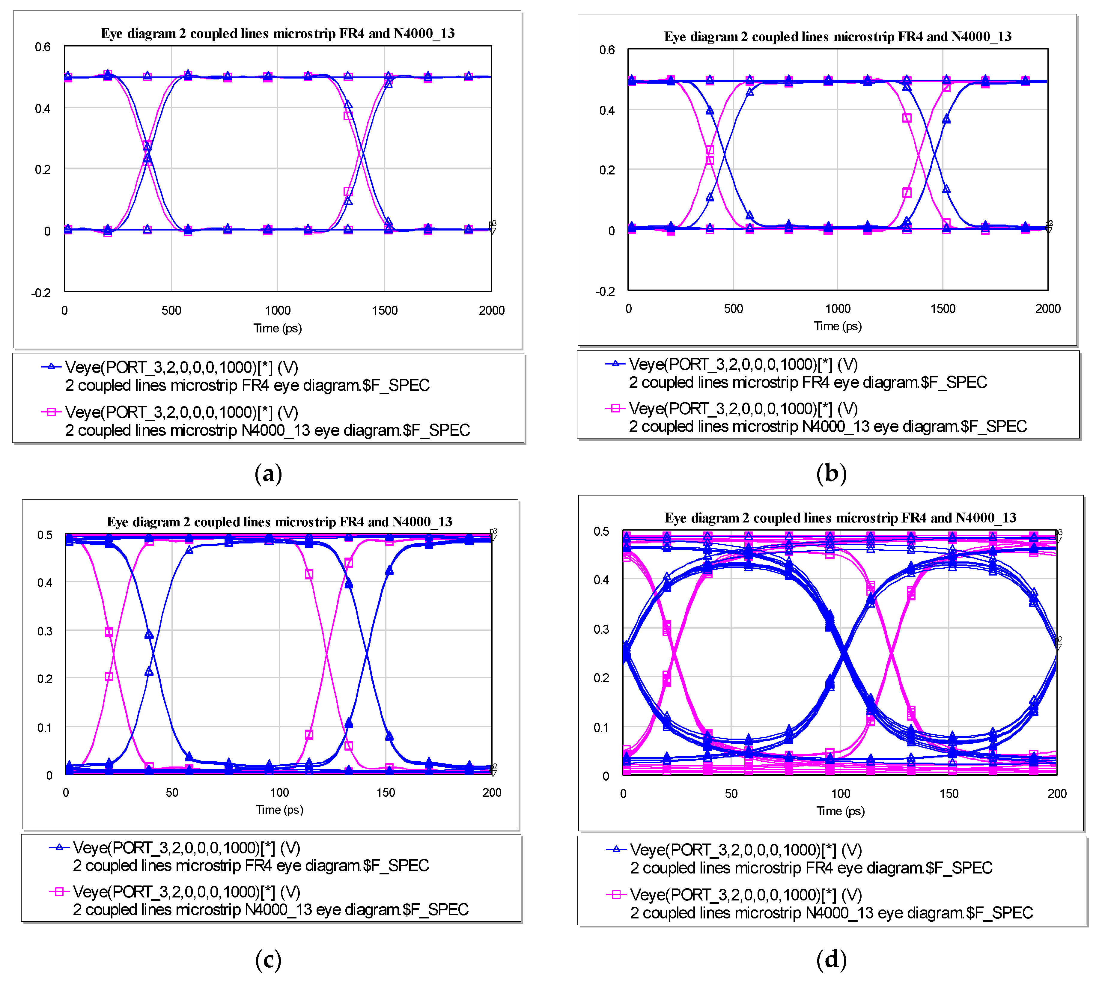
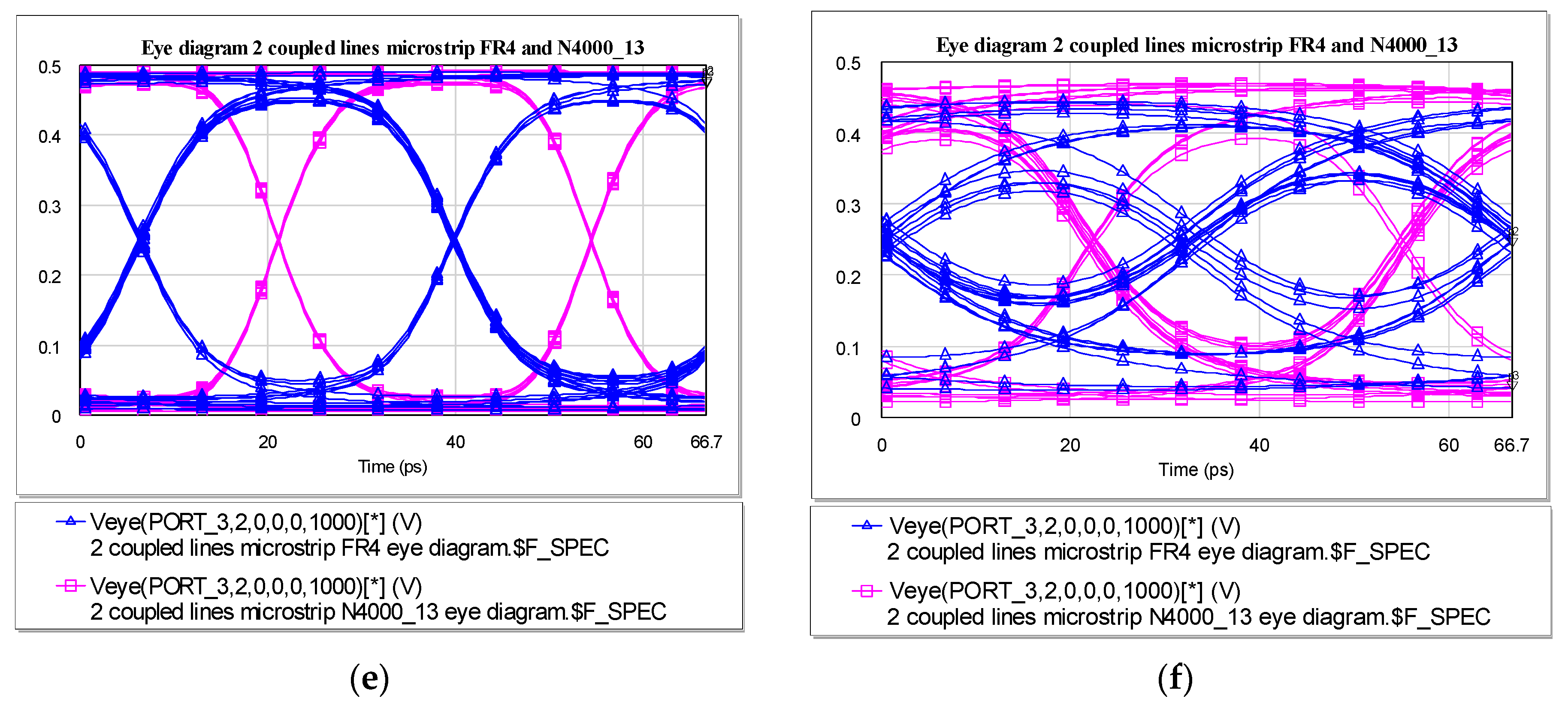
(a) Eye diagram for two coupled microstrip lines with L = 60 mm and Rate = 1 GHz. (b) Eye diagram for two coupled microstrip lines with L = 250 mm and Rate = 1 GHz. (c) Eye diagram for two coupled microstrip lines with L = 60 mm and Rate = 10 GHz. (d) Eye diagram for two coupled microstrip lines with L = 250 mm and Rate = 10 GHz. (e) Eye diagram for two coupled microstrip lines with L = 60 mm and Rate = 30 GHz. (f) Eye diagram for two coupled microstrip lines with L = 250 mm and Rate = 30 GHz.
We modified all the other circuits in the same way and, based on the results obtained, we performed an analysis in the time domain using the eye diagram. First, we evaluated the voltage at port 3, and considered in this case the differential output of the circuits designed in microstrip technology for both types of substrates. Simulations for different frequency rates and line lengths were performed because we wanted to observe the behavior of the circuits as the line length increased, and also as the rate increased.
The eye diagrams are graphical representations used in signal processing and telecommunications to assess the quality and integrity of digital signals. They are particularly valuable in high-speed communication systems. An eye diagram is formed by overlaying multiple signal periods on top of each other, creating a visual representation of signal quality. The resulting pattern typically resembles an “eye,” hence the name. The horizontal axis represents time, while the vertical axis represents signal amplitude.
Key aspects of eye diagrams include opening width, rise and fall times, jitter, and noise. The width of the “eye” opening indicates signal timing and the potential for timing errors. Rise and fall times, often measured at the edges of the eye, represent the speed at which the signal transitions between its high and low states. Deviations from the ideal eye shape indicate the presence of jitter (timing variations) and noise, both of which can affect signal reliability.
The clearer and wider the eye opening, the better the signal quality. Engineers use eye diagrams to quickly assess and troubleshoot signal integrity issues, making them a valuable tool in optimizing communication systems, especially those operating at high data rates.
As shown in Figure 9, the simulations were performed for two values of line lengths, more precisely, for L = 60 mm and L = 250 mm, respectively. Also, we used three data rates, namely, {1 GHz, 10 GHz, 30 GHz}. In the eye diagrams, shown in Figure 9, blue is the result obtained for the circuit with substrate FR4 and pink is the result corresponding to the circuit with substrate N4000-13. Analyzing the results, we noticed how the eye closes as the line length increased and as the rate increased. At low rates and small lengths of the transmission line, the eye is open. We noticed that for a length of 250 mm and a rate of 30 GHz, the eye diagram associated with the FR4 substrate circuit was completely distorted.
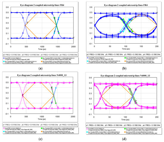
Figure 9.
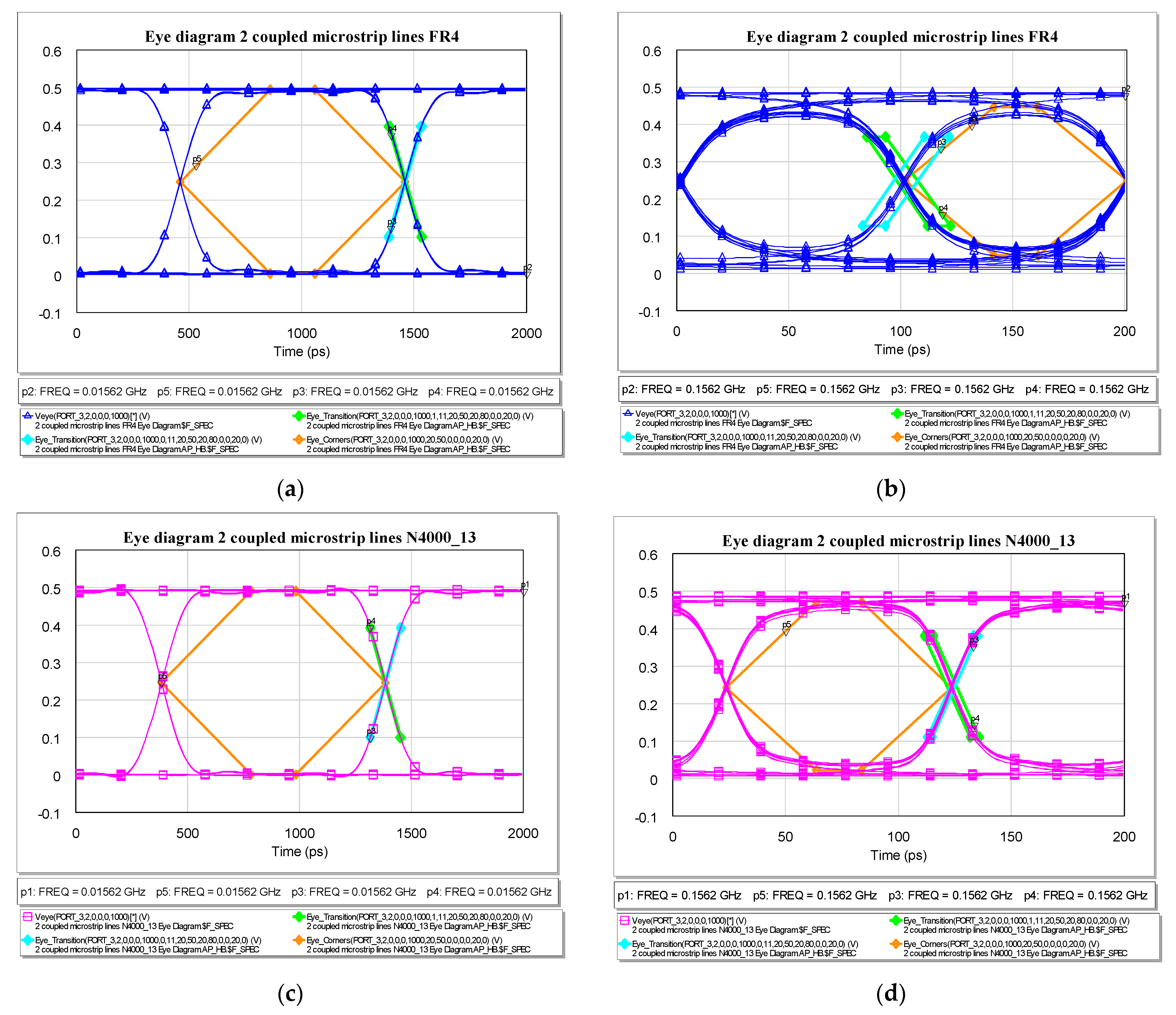
(a) Rise time, fall time, and corners on the eye diagram for two coupled microstrip lines and FR4 substrate for L = 250 mm and Rate = 1 GHz. (b) Rise time, fall time, and corners on the eye diagram for two coupled microstrip lines and FR4 substrate for L = 250 mm and Rate = 10 GHz. (c) Rise time, fall time, and corners on the eye diagram for two coupled microstrip lines and FR4 substrate for L = 250 mm and Rate = 1 GHz. (d) Rise time, fall time, and corners on the eye diagram for two coupled microstrip lines and FR4 substrate for L = 250 mm and Rate = 10 GHz.
Based on the eye diagram representations, we extracted details about the rise and fall time and jitter. We simulated these three parameters on separate diagrams for the two substrates used. The simulations were performed for a length of 250 mm at two frequency rates: 1 GHz and 10 GHz.
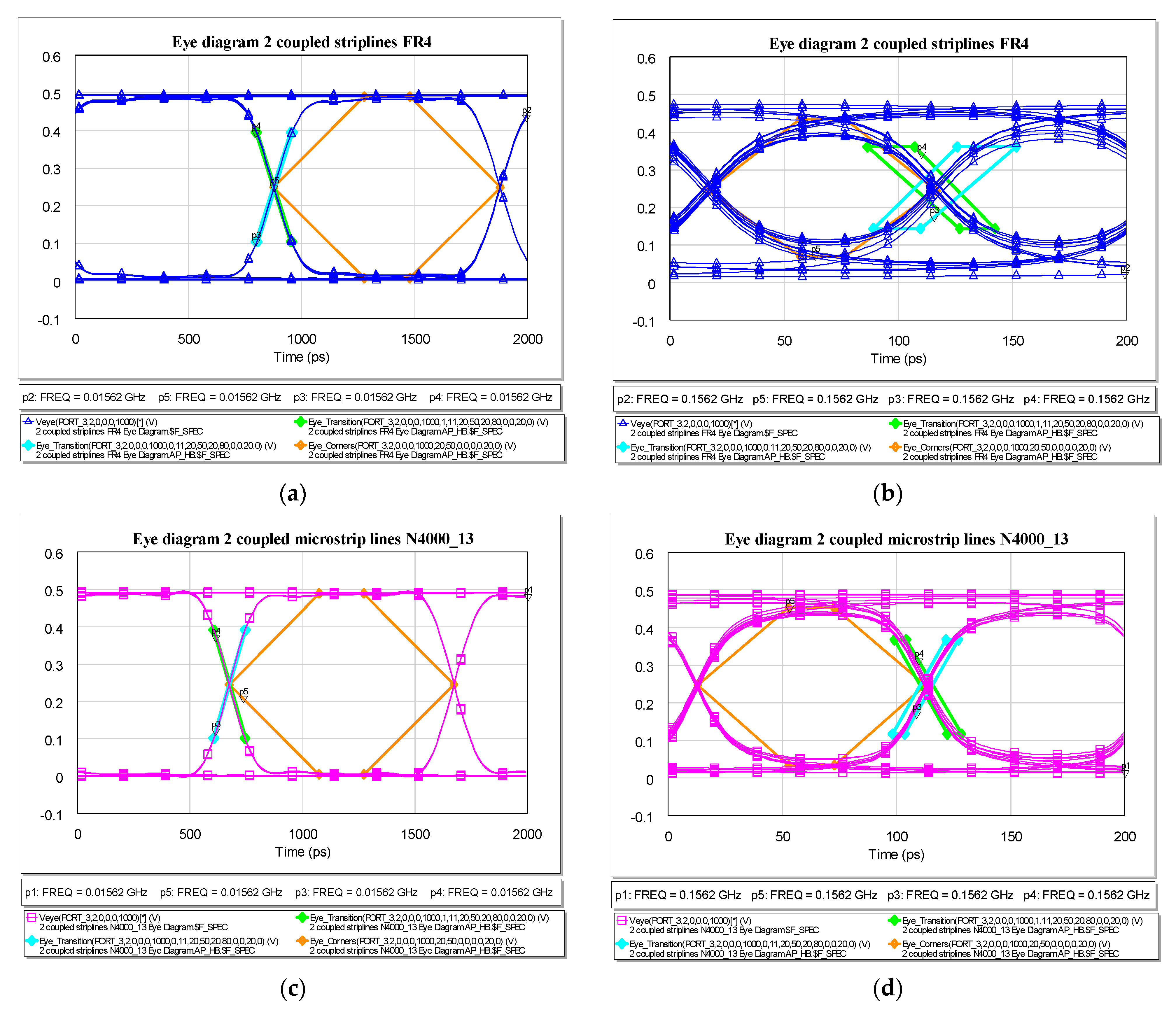
Figure 10a,b show the results for the FR4 substrate and Figure 10c,d show the results for the N4000-13 substrate. In all four figures, the rising time is marked with light blue, the falling time is marked with green, and the corners of the eye are marked with orange. At a rate of 1 GHz, we noticed that we have a single line for the rise time and one for the fall time, which suggests that the transition is made through a single point, leading to the minimum value achieved for jitter. With the increase of the frequency rate to 10 GHz, we noticed that the transitions were made through several points, both for the rise time and for the fall time, with more green and light blue lines appearing.
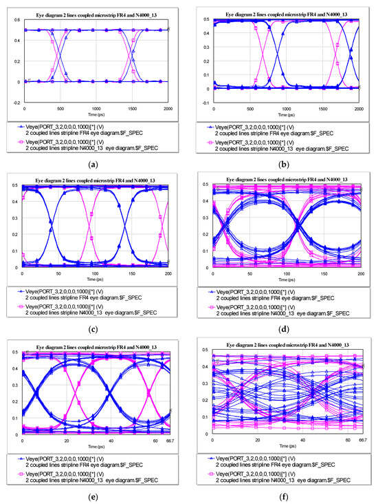
Figure 10.
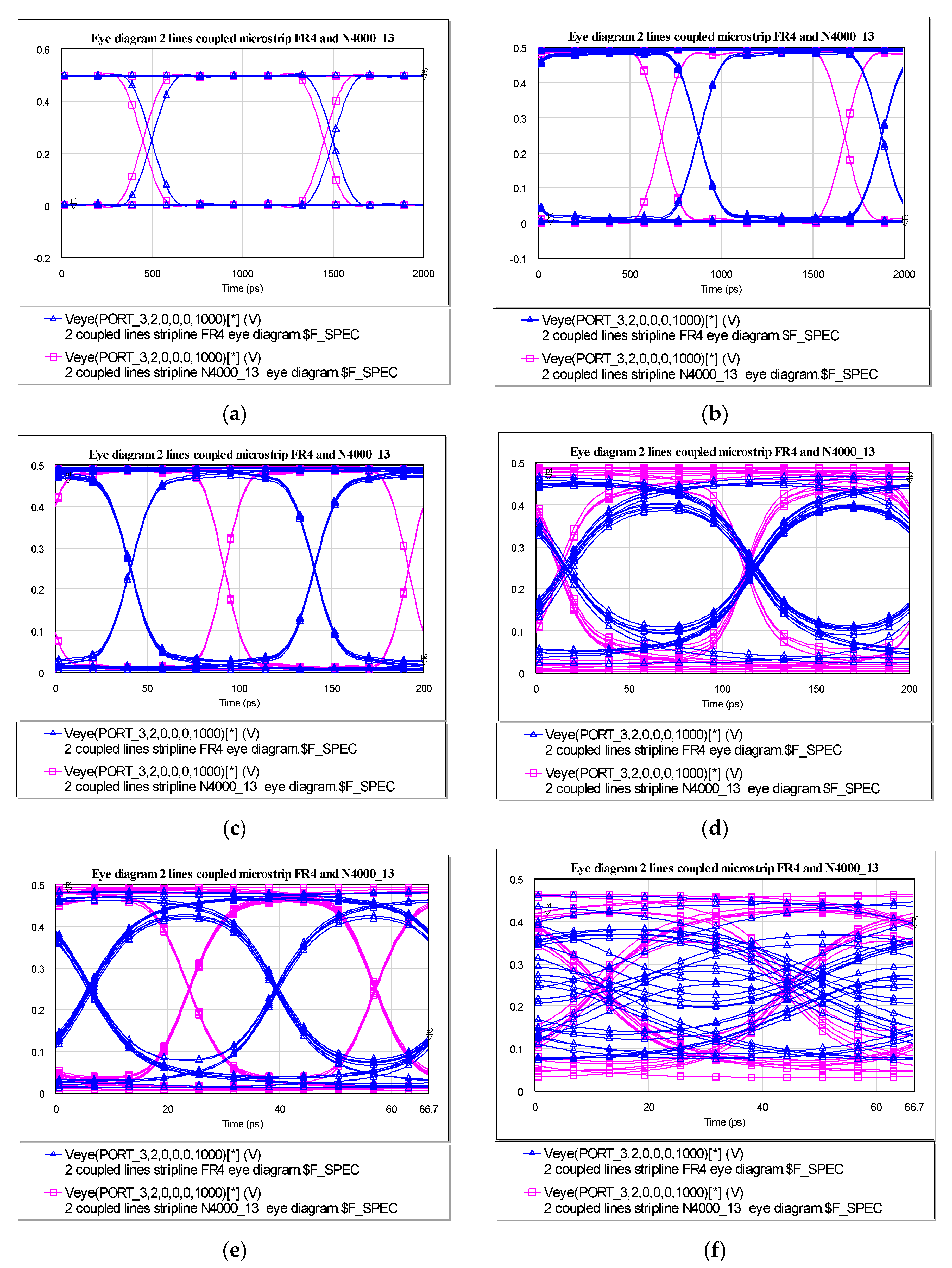
(a) Eye diagram for two coupled lines, stripline technology for L = 60 mm and Rate = 1 GHz. (b) Eye diagram for two coupled lines, stripline technology for L = 250 mm and Rate = 1 GHz. (c) Eye diagram for two coupled lines, stripline technology for L = 60 mm and Rate = 10 GHz. (d) Eye diagram for two coupled lines, stripline technology for L = 250 mm and Rate = 10 GHz. (e) Eye diagram for two coupled lines, stripline technology for L = 60 mm and Rate = 30 GHz. (f) Eye diagram for two coupled lines, stripline technology for L = 250 mm and Rate = 30 GHz.
Based on the simulation results concerning the corners of the eye, we observed that the transition takes place through the corners of the eye, which again suggests a minimum jitter value. For a rate of 10 GHz, we can see that the mask is exceeded both for the upper level and for the lower level.
Values were obtained for the transition on rise time and fall time for both materials at the two rates at which the simulations were performed (1 GHz and 10 GHz) for microstrip lines. The corresponding rise and fall time values can be extracted similarly. For we obtained for rise time and for fall time, respectively, for FR4, and for N4000-13, we gained better values and . For higher data rates (), the values decreased as follows: and for FR4 and and for N4000-13.
Values were obtained for time and amplitude for the eye mask. The simulations were carried out for FR4 and N4000-13 materials at a rate of 1 GHz and 10 GHz for microstrip technology. The results were presented for each substrate and for the two frequencies, the values of crossing points for time (ps) and associated voltage (V) were obtained. For better understanding, we can explain the corners values on Figure 10a, the orange measurement trace (hexagonal shape). We have six plus one (as return) crossing points as follows: starting from the left crossing point, two level one edges, right crossing point, and two level zero edges, and return on the left crossing point. The values are given by the mean, but another representation could have been the standard deviation, for example. For the results for the eye diagram conclude to the same observation for corners tabular representation, meaning that both substrates present similar behavior, having values for the corners with the same mean seen in Figure 10, with similar eye opening. Increasing the rate, we can observe a degradation on the eye opening in Figure 10, also highlighted by the values of the corners with a higher range of minimum and maximum values means for N4000-13 compared to those of FR4. The results for transitions and eye corners are illustrated in Appendix A.
Another measurement in the time domain is the jitter metric that is computed on the eye diagram. Jitter refers to the deviation or variability in the timing of signals in a communication system. It is a phenomenon characterized by small, rapid, and unpredictable variations in the timing of signal edges. Jitter can occur in various electronic and communication systems, affecting the accuracy and stability of signal transmission. In digital communications, jitter can lead to timing errors, signal distortion, and decreased system performance. Thus, managing and minimizing jitter is crucial in ensuring reliable and efficient data transfer, especially in high-speed communication systems. Jitter can be determined by the peak-to-peak value or by the root mean square value. Table 1 shows the peak-to-peak jitter at the same frequencies for FR4 and N4000-14 materials for stripline technology for and . It was determined from the maximum between the values on the horizontal axis (time in ps) of the two crossing points of the eye diagram, with each one considered as the difference from the upper and lower peak values. The results demonstrate a slightly better stability, with an increase of frequency for N4000-13 compared to the traditional FR4 substrate as jitter increased for both substrates with the frequency, but for FR4, the increase was 23.25% and 11.76% for N4000-13.

Table 1.
Jitter values for microstrip lines extracted from simulation results.
Using the FR4 substrate designed in stripline technology and with a pseudo-random signal source at the input port, we represented the overlapping eye diagrams for the output port of the circuits, as shown in Figure 11. The results corresponding to the circuit with substrate FR4 are illustrated in blue, while those corresponding to the circuit with substrate N4000-13 are in pink. The simulations were performed at the same frequency rates and the same transmission line lengths as in the case of microstrip technology for proper comparison.
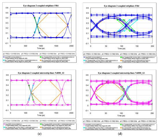
Figure 11.
(a) Rise time, fall time, and corners on the eye diagram for two coupled striplines, FR4 substrate for L = 250 mm and Rate = 1 GHz. (b) Rise time, fall time, and corners on the eye diagram for two coupled striplines, FR4 substrate for L = 250 mm and Rate = 10 GHz. (c) Rise time, fall time, and corners on the eye diagram for two coupled striplines, FR4 substrate for L = 250 mm and Rate = 1 GHz. (d) Rise time, fall time, and corners on the eye diagram for two coupled striplines, FR4 substrate for L = 250 mm and Rate = 10 GHz.
Analyzing the results presented above, we notice that even in the case of stripline technology for large rates and lengths, the signal is degraded. We notice that the performance degrades even for smaller rates and line lengths for the circuit with FR4 substrate compared to the circuit on N4000-13 substrate.
Therefore, comparing all the results obtained in Figure 9 and Figure 11, we notice a better behavior at high frequencies and lengths for circuits with substrate N4000-13 compared to circuits with substrate FR4. We chose to increase the length of the line and to study the behavior of the circuits in this case, because its increase leads to the occurrence of the attenuation phenomenon due to the loss tangent of the dielectric. On the other hand, increasing the transmission rate of symbols reduces the transmission time of the signals. We demonstrated that as the frequency rate increased from 1 GHz to 30 GHz, the signal transmission time decreased from 2000 ps to approximately 67 ps in both cases.
The same simulations were carried out for the rise time, the fall time, and the corners of the eye, and for the stripline technology, as shown in Figure 12. The same lengths and frequency rates were used as in the previous case.

Figure 12.
N4000-13 two-line uncoupled circuit and substrate designed in microstrip technology and pseudo-random signal source.
Figure 11a,b show the results for the FR4 substrate and Figure 11c,d show the results for the N4000-13 substrate in stripline technology. In all four figures, the rising time is represented with light blue, the falling time is represented with green, and the corners of the eye are represented with orange. We notice that the performance of the circuits has not changed much. At a rate of 1 GHz, we still have a fast transition, which indicates a very low jitter value, and with the increase in the frequency rate, the jitter value also increased. As the rate increases, we see how the transitions on the upper and lower levels exceed the eye mask.
Results were obtained for time and amplitude for the transition of rise and fall time for the FR4 and N4000-13 materials for the lines designed in stripline technology for different data rates. The corresponding rise and fall time values can be extracted in a similar manner. For we obtained for rise time and for fall time, respectively, for FR4, and for N4000-13, we gained better values and . For higher data rates (), the values decreased as follows: and for FR4 and and for N4000-13.
A few parameters are available for analysis, extracted from jitter measurements. Among these, the most important is the time variation of the voltage. As we have two intervals or two eye crossings for representation, both rise and fall times will include, in pairs, values for each unit interval. These might be different and will be seen as jitter—eye transition variation voltage. Measurements of rise and fall times are set between 20% and 80% and can be modified. The measurement of the transition contains individual values for different means as follows: left and right mean, left and right sigma (standard deviation), and left and right lower and upper peaks. In Figure 11d, the curves in light green and blue contain the above-mentioned measurement points, but another type of representation of these transitions is in a tabular form. On each line in the table, we have the values for the two standard deviations, two means, and return on the first instance. This explains the coincidence of the first and last line in each section, for each substrate, and for each frequency.
Results were obtained of the simulations for the corners of the eye for the same materials and frequency rates as above, for stripline technology. The results were presented for each substrate and for the two frequencies, the values of crossing points for time (ps) and associated voltage (V) were obtained. For better understanding, we can explain the corners values on Figure 11a, the orange measurement trace (hexagonal shape). We have six plus one (as return) crossing points as follows: starting from the left crossing point, two level one edges, right crossing point, and two level zero edges, and return on the left crossing point. The values are given by the mean, but another representation could have been the standard deviation, for example. For the results for the eye diagram conclude to the same observation for corners tabular representation, meaning that both substrates present similar behavior, having values for the corners with the same mean seen in Figure 11, with similar eye opening. Increasing the rate, we can observe a degradation on the eye opening in Figure 11, also highlighted by the values of the corners with a higher range of minimum and maximum values means for N4000-13 compared to those of FR4. The results for transitions and eye corners in the case of stripline interconnections are illustrated in Appendix B.
Table 2 shows the peak-to-peak jitter at the same frequencies for FR4 and N4000-14 materials for stripline technology for and . Again, the results demonstrate the better stability, with an increase of frequency for N4000-13 compared to the traditional FR4 substrate, as jitter increased for both substrates with the frequency but, for FR4, the increase was 65.53% and only 6.65% for N4000-13.

Table 2.
Jitter values for stripline lines extracted from simulation results.
We notice that in this case we also have a lower jitter value for the circuit with the N4000-13 substrate. This means that regardless of the design technology, microstrip or stripline, FR4 substrate circuits achieve a higher jitter value that will degrade circuit performances.
Minimizing jitter in a system brings several benefits. Firstly, it enhances the overall reliability of signal transmission by reducing timing uncertainties, ensuring that data arrives at their destination consistently and predictably. This is particularly crucial in applications where precise timing is essential, such as telecommunications and data networking. Secondly, a low jitter value contributes to improved signal integrity, reducing the likelihood of timing errors and distortion. This is especially important in high-speed digital communication systems, where even small variations in signal timing can lead to data corruption. On the other hand, minimizing jitter is a key to achieving stable and accurate synchronization between different components within a system. In scenarios like audio and video streaming or real-time data processing, maintaining a low jitter level helps prevent synchronization issues and ensures a smooth and seamless user experience.
In conclusion, achieving a minimal jitter value is essential for maintaining the reliability, integrity, and synchronization of signals in various communication and electronic systems.
2.2. The Fiberglass Fabrics Effect
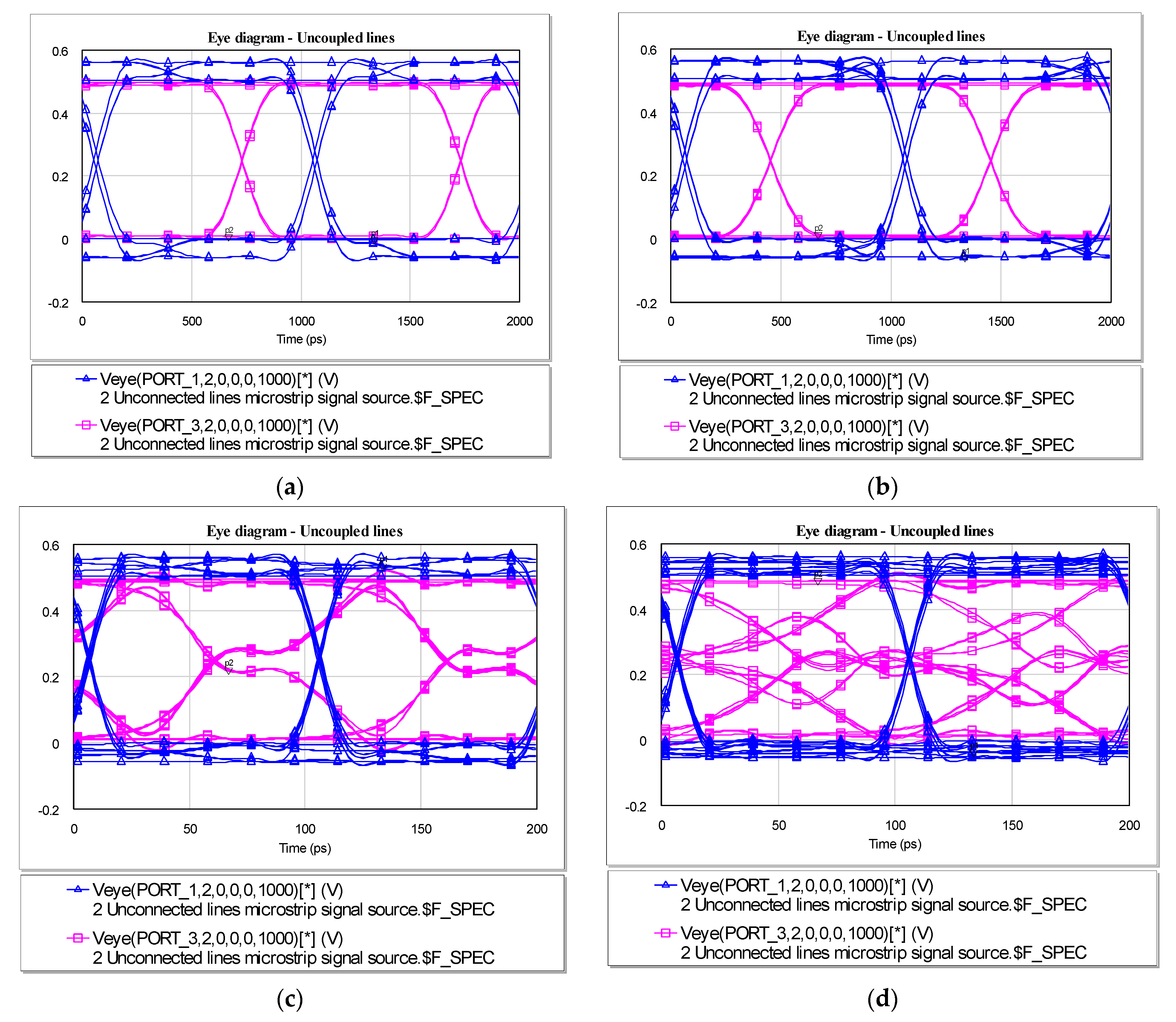
Based on previous coupled line models, we created circuits with two separate lines to analyze the impact of glass fiber fabrics. These circuits feature composite substrates and will be simulated using N4000-13 material for lengths of 120 mm and 250 mm at 1 GHz and 10 GHz rates, with the results analyzed using eye diagrams, as illustrated in Figure 13.
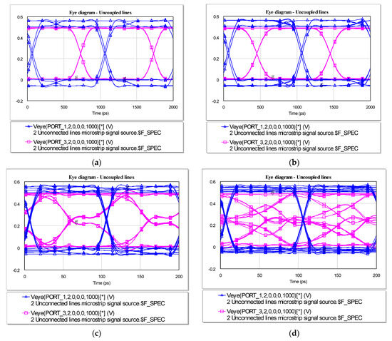
Figure 13.
(a) Eye diagram for two non-coupled microstrip lines for L = 120 mm and Rate = 1 GHz. (b) Eye diagram for two non-coupled microstrip lines for L = 250 mm and Rate = 1 GHz. (c) Eye diagram for two non-coupled microstrip lines for L = 120 mm and Rate = 10 GHz. (d) Eye diagram for two non-coupled microstrip lines for L = 250 mm and Rate = 10 GHz.
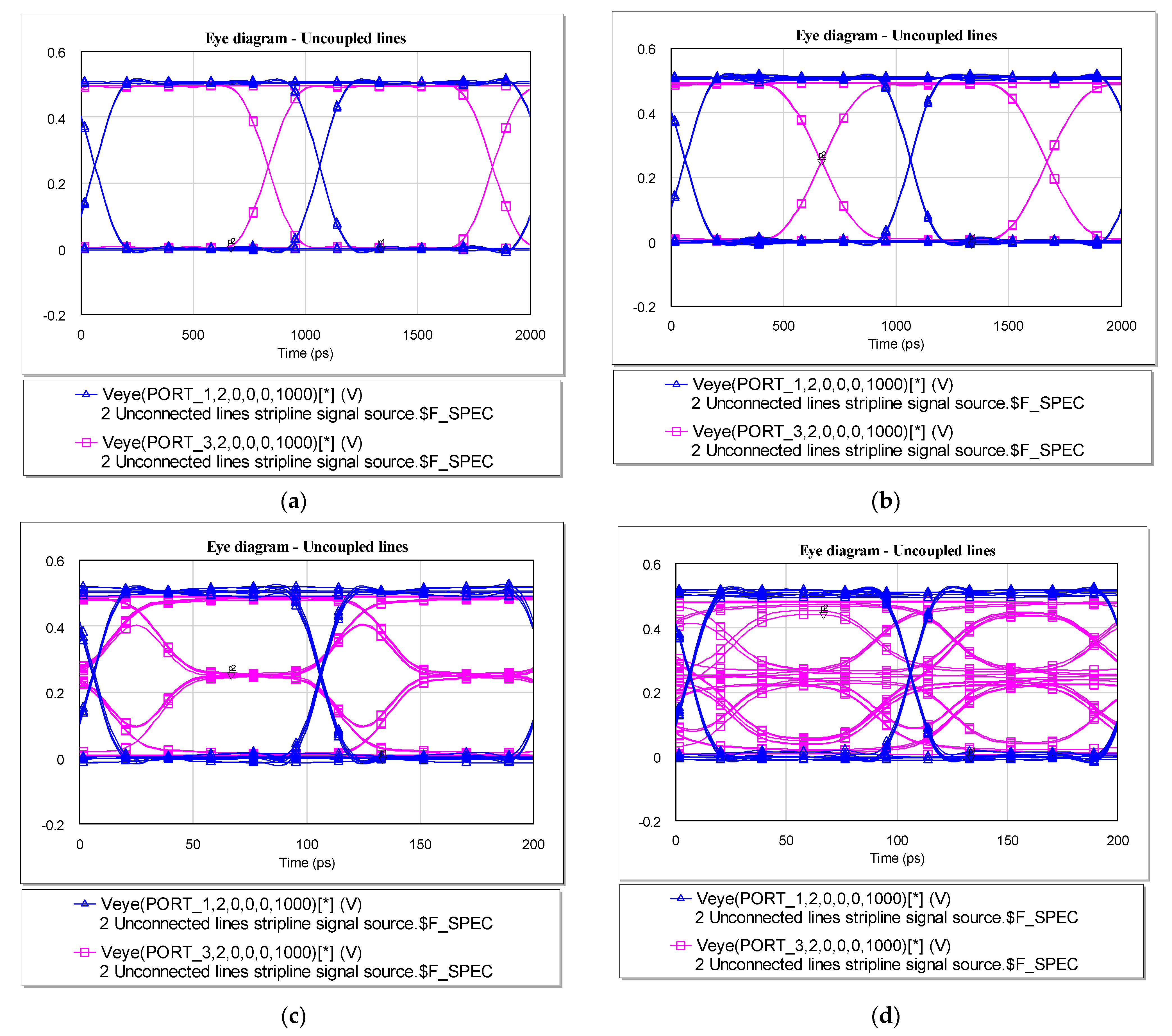
Figure 14 shows the results obtained by overlapping the eye diagrams of the signal at the circuit input and the results obtained after passing through the transmission line. Analyzing the images, we notice that, as the rate of the transmitted signal increases, the eye diagram closes. Therefore, at rates of 10 GHz and interconnection lengths of 250 mm, the eye diagram is completely degraded. The input signal is represented in blue and the signal at the end of the line is represented in pink. For low rates, such as 1 GHz, the eye diagram maintains both its amplitude and jitter level, and at high interconnection values.
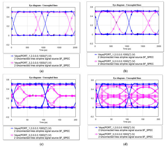
Figure 14.
(a) Eye diagram for two non-coupled stripline lines for L = 120 mm and Rate = 1 GHz. (b) Eye diagram for two non-coupled stripline lines for L = 250 mm and Rate = 1 GHz. (c) Eye diagram for two non-coupled stripline lines for L = 120 mm and Rate = 10 GHz. (d) Eye diagram for two non-coupled stripline lines for L = 250 mm and Rate = 10 GHz.
Next, we implemented the two uncoupled lines circuit stripline technology, but with pseudo-random signal source, and the eye diagrams associated with the circuit are shown in Figure 12. It can be observed, again, that as the transmitted signal rate increases, the eye diagram closes, so at 10 GHz and an interconnection length of 250 mm, the eye diagram is completely degraded, represented in pink in Figure 14 in all four cases at the far end of the evaluated interconnection. For lower rates, such as 1 GHz, the eye diagram maintains both its amplitude and jitter level for longer interconnections lines.
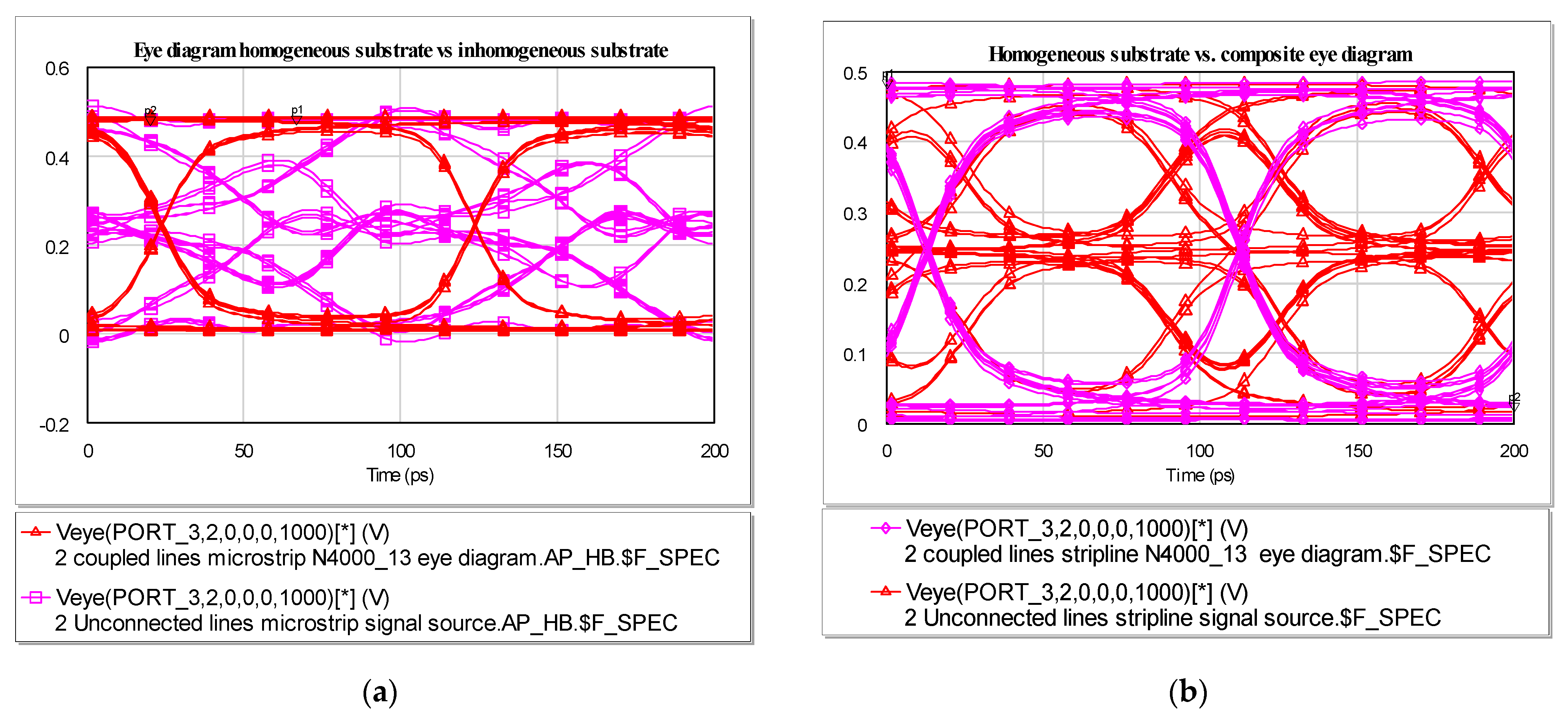
A comparison can be made on the same system of the shape of the eye diagram obtained at the far end of the interconnection by overlapping the graphs maintaining the rate and length of the interconnection for circuits with homogeneous and composite substrate, respectively. First, the result obtained for the use of microstrip technology is illustrated.
We notice that the circuit with homogeneous substrate, represented by red in Figure 15, behaves better than the circuit made with inhomogeneous substrate, represented by pink. In the case of the second circuit, the eye closes faster, and the presence of distortions is observed. The following is an illustration of the overlap of eye diagrams for stripline technology.
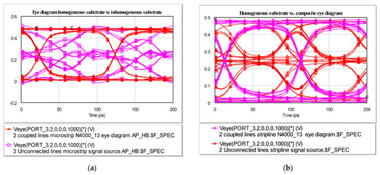
Figure 15.
(a) Eye diagram homogeneous substrate vs. inhomogeneous substrate—microstrip. (b) Eye diagram homogeneous substrate vs. inhomogeneous substrate—stripline.
Figure 15 shows that in the case of the composite substrate, represented in red, the eye diagram shows a higher jitter value compared to the circuit that has a homogeneous substrate, represented in pink.
Time domain analysis and frequency domain analysis are two distinct approaches in the study of signals and systems. Time domain analysis is a method that examines the behavior of signals over time, focusing on how the signal varies over time and the temporal relationships between different signal events. The primary advantages of this analysis include detecting specific events within a time interval and evaluating the system’s response over time. However, this method has limitations, such as not providing direct information about the frequency content of the signal.
Frequency domain analysis is a method that investigates the frequency content of signals, revealing the frequency components that make up a signal and their intensity. The advantages of frequency domain analysis lie in studying the frequency spectrum, identifying dominant frequencies, and evaluating how a system responds to different frequencies. However, it is limited by its inability to provide information about the timing or sequence of events over time.
Therefore, it is crucial to study both cases. Time domain analysis and frequency domain analysis offer different perspectives on system behavior. Combining both methods provides a more comprehensive understanding. Some faults or issues may be more evident in a time domain analysis, while others may be better understood by exploring their frequency content. In the design and analysis of systems, understanding behavior in both domains can contribute to optimizing performance and stabilizing the system. By approaching both methods, more robust and complete conclusions can be drawn about the characteristics of the analyzed signals and systems.
Article [1] presented only frequency domain analysis. We have centralized the results obtained in [1] in two tables: Table 3 for reflections loss and Table 4 for insertion loss.

Table 3.
S parameters for stripline and microstrip.

Table 4.
Insertion loss for stripline and microstrip for various interconnections’ lengths.
As mentioned in [1], a stripline interconnection presents improved reflection loss compared to a microstrip interconnection and, as can be seen in Table 3, we have a reduced value for reflection loss for stripline, 68 dB, compared to 41 dB for microstrip technology in differential mode. The difference is much lower between the two technologies for common mode: 48 dB vs. 46 dB.
As mentioned in [1], the number of resonance frequencies increased with the length of interconnection for both microstrip and stripline technology. As was demonstrated in the case of stripline, we had additional frequencies of resonance compared to microstrip technology: three resonances for microstrip compared to four resonances for stripline at 200 mm or four resonances vs. five resonances for 250 mm for the same technologies, as seen in Table 4.
For a given interconnection on a PCB, we can evaluate the skew that is unintentionally induced in a differential pair due to the misalignment of conductors and glass fiber bundles in PCB substrates [37]. In [38], it was demonstrated that wider traces will see less variation of these metrics compared to narrow traces and recommended to apply the proposed numerical experiment on each case. We can also evaluate the crosstalk due to a tight separation between routes; this behavior is evaluated via S parameters, with detection of a signal from a trace to another, even if the power level is small enough. This traditional technique is widely used for electromagnetic and acoustic communications, as in [39].
Besides frequency analyses, we demonstrated that, even though the stripline technology is a more lossy medium, it does not distort the signal as much as the microstrip variant, especially with the increase of data rates. In Chapter 3, we analyzed the corresponding substrates, FR4 and N4000-13, in the time domain and showed that the traditional FR4 substrate has an increase of jitter, with an increase of frequency for both microstrip and stripline interconnections much more important compared to N4000-13. The distortion of the signal is illustrated in Figure 13a,b for microstrip at 1 GHz compared to Figure 14a,b for stripline at the same rate. With the increase of frequency, to 10 GHz, the stripline wave form and the corresponding eye diagram presents low jitter and low overshoot and undershoot, while for the microstrip lines, these parameters increase. The values of jitter are presented in Table 1 for microstrip and in Table 2 for stripline, while transition rise and fall time and eye corners are summarized in Appendix A and Appendix B for the two frequencies. The jitter value for microstrip at 1 GHz is 1.117 ps and at 10 GHz is 1.2659 ps, showing an increasing of jitter of 11.76% compared to 1.8578 ps at 1 GHz and 1.9901 ps for 10 GHz for the stripline, representing a 6.65% increase of jitter with the increase of frequency.
The results presented in [1], together with the results from our present paper, allow a complete study of a given material for both microstrip and stripline technology, as both frequency and time domain analysis will provide particularities either for reflection loss, insertion loss, number of resonance frequencies, or jitter with the increase of data rates.
3. Discussion and Future Work
In this article, we presented the circuits made in the MWO work environment from AWR DE. We simulated circuits with two coupled lines designed in microstrip and stripline technology for two types of materials: FR4 and N4000-13.
The results obtained in this article represent the continuation of the study initiated in [1] and provide further insights into how the occurrence of FWE can be prevented and how it affects circuit performance. Further developing the setup established in our previous work, we extended our research and conducted FWE studies in both time and frequency domains for different substrate materials. In the frequency domain, the simulations were based on representing the S parameters based on the Smith diagrams, which helped us assess circuit matching. These simulations were conducted for both microstrip and stripline technologies, using both FR4 and N4000-13 materials. We compared the results from various design technologies and material choices. To emphasize the findings from [1], we further explored the time domain, this time using eye diagrams. While in the previous paper the focus was placed on presenting the reflection coefficients for the common and differential mode and the insertion losses for different lengths of the microstrip line, in this paper, an emphasis was put on the time domain representation in the signal at the output of the line when the input was connected at a pseudo-random signal source. Based on the eye-diagrams obtained, we drew several interesting conclusions regarding the rise time, fall time, and jitter. Simulations were conducted for all the cases mentioned above and results were compared to provide a comprehensive understanding of FWE in circuit design.
First, we checked the matching of the circuits with the help of the distribution parameters that we represented on the Smith chart. We noticed how these parameters were in the middle of the Smith chart, which means that the circuits are matched. To check the performance of the circuits, we performed simulations in the time domain using the eye diagram representation. We simulated the circuits at three different frequency rates (1 GHz, 10 GHz, and 30 GHz) for two line lengths (60 mm and 250 mm). Comparing these results, we noticed that the circuits designed in stripline technology offered better performances, with the simulation results being more favorable. This happened because, in the case of microstrip technology, the transmission occurs through the air, and this leads to the appearance of coupling on the neighboring line. Based on the obtained eye diagrams, we were able to extract data about the rise time and the fall time. It was highlighted that with the increase of the frequency rate (from 1 GHz to 10 GHz), the transition from the upper front to the lower levels was no longer performed through a single point, as it happened at a rate of 1 GHz. Also, we demonstrated how with the increase of the frequency rate, the upper and lower levels exceeded the eye mask. Given the results, we noticed that N4000-13 presents a lower variation of the rise and fall time for microstrip technology, 16.67%, compared to FR4 substrate’s 27.50% (values obtained for ). We noticed that the jitter values were lower for circuits with N4000-13 material compared to circuits with FR4 material. The simulations showed that for stripline technology, the jitter for N4000-13 presented a lower increase in comparison to microstrip technology (6.65% vs. 11.76%) with the increase of frequency. For microstrip, the jitter was lower compared to stripline technology, but the influence of the frequency increase had a lower impact on the N4000-13 substrate.
We performed simulations in the time domain using the eye diagram for rates of 1 GHz and 10 GHz and for lengths of 120 mm and 250 mm. To highlight the influence of the high data rates, the frequency of the data source varied from 1 GHz, for small rates, to 10 GHz, for high rates. The interconnection lengths’ selection, single-ended or coupled, was made between 120 mm and 250 mm, since these are typical lengths on backplanes where signal integrity issues must be considered. Higher frequencies and higher lengths will be analyzed in our future work. With the increase in length and frequency rate, the eye closed and more distortions appeared. Therefore, the performance of the circuits was lower in this case.
After all the simulations were carried out and based on the results obtained, we noticed how important was both the technology in which a circuit was designed and also the material we used. The stripline technology offers higher performance to the circuits, because the microstrip technology has a much higher emission rate, and this leads to the propagation of the signal on the neighboring line. Also, FWE can be fixed if it is noticed in time and the performance of the circuits can be improved.
The main contribution consisted of the implementation of the circuits in the MWO design tool from AWR-DE; the selection of the specifications parameters for two substrates; a low-cost, conventional FR4 and a high-speed-oriented substrate, N4000-13, from the data sheets; and the implementation and analysis of the circuits. Both time and frequency domain simulations were performed, with the extraction of data from these simulations presented in detail in the Results section.
In conclusion, in order to benefit from the highest possible performance for a given circuit, it is recommended to carry out an early verification of the impact of the effect of the fiber fabrics on the designed circuit, since it has been demonstrated through the simulations that the composite substrate influences, together with the increase in the frequency rate, the closing of the eye and encourages the appearance of distortion and interference.
Author Contributions
Conceptualization, M.S.-D., D.B. and S.H.; methodology, M.S.-D. and S.H.; software, M.S.-D. and D.B.; validation, M.S.-D. and D.B.; formal analysis, S.H.; writing—original draft preparation, M.S.-D., D.B. and S.H.; writing—review and editing, M.S.-D., D.B. and S.H.; visualization, M.S.-D. and D.B.; supervision, D.B. and S.H. All authors have read and agreed to the published version of the manuscript.
Funding
This research received no external funding.
Data Availability Statement
All the results are contained within the article and the Appendix A and Appendix B.
Conflicts of Interest
The authors declare no conflict of interest.
Abbreviations
The following abbreviations were used in this manuscript:
| AME | Additively Manufactured Electronics |
| AWR DE | Applied Wave Research Design Environment |
| CT | Computer Tomography |
| EM | Electromagnetic |
| FRCM | Fiber–Resin Composite Materials |
| FWE | Fiber Weave Effect |
| GBPS | Gigabits Per Second |
| HT | Hilbert Transform |
| IoT | Internet of Things |
| MWO | Microwave Office |
| PCB | Printed Circuit Board |
Appendix A

Table A1.
Transition rise and fall time values for microstrip lines extracted from simulation results.
Table A1.
Transition rise and fall time values for microstrip lines extracted from simulation results.
| Rate | Substrate | Transition Rise Time (ps) | Transition Fall Time (ps) | ||
|---|---|---|---|---|---|
| Time (ps) | Voltage (V) | Time (ps) | Voltage (V) | ||
| 1 GHz | FR4 | 1387.7 | 0.10352 | 1387.9 | 0.3951 |
| 1391.8 | 0.10352 | 1390.9 | 0.3951 | ||
| 1535.2 | 0.3951 | 1534.4 | 0.10352 | ||
| 1531.1 | 0.3951 | 1531.2 | 0.10352 | ||
| 1387.7 | 0.10352 | 1387.9 | 0.3951 | ||
| N4000-13 | 1314.4 | 0.10061 | 1315.4 | 0.39423 | |
| 1316.7 | 0.10061 | 1316.4 | 0.39423 | ||
| 1453.2 | 0.39423 | 1453.2 | 0.10061 | ||
| 1450.1 | 0.39423 | 1451 | 0.10061 | ||
| 1314.4 | 0.10061 | 1315.4 | 0.39423 | ||
| 10 GHz | FR4 | 88.463 | 0.12823 | 82.899 | 0.37586 |
| 92.257 | 0.12823 | 90.551 | 0.37586 | ||
| 122.67 | 0.37586 | 118.19 | 0.12823 | ||
| 112.05 | 0.37586 | 113.23 | 0.12823 | ||
| 83.463 | 0.12823 | 82.899 | 0.37586 | ||
| N4000-13 | 112.4 | 0.11444 | 112.5 | 0.38174 | |
| 115.67 | 0.11444 | 115.56 | 0.38174 | ||
| 135.82 | 0.38174 | 135.61 | 0.11444 | ||
| 132.39 | 0.38174 | 132.46 | 0.11444 | ||
| 112.4 | 0.11444 | 112.5 | 0.38174 | ||

Table A2.
Eye corners values for microstrip lines extracted from simulation results.
Table A2.
Eye corners values for microstrip lines extracted from simulation results.
| Substrate | 1 GHz | 10 GHz | ||
|---|---|---|---|---|
| Time (ps) | Voltage (V) | Time (ps) | Voltage (V) | |
| FR4 | 461.01 | 0.2486 | 1.5158 | 0.2491 |
| 860.72 | 0.49303 | 41.508 | 0.4584 | |
| 1060.6 | 0.49303 | 61.505 | 0.4584 | |
| 1460.3 | 0.2486 | 101.5 | 0.2491 | |
| 1060.6 | 0.0063951 | 61.505 | 0.045687 | |
| 860.72 | 0.0063951 | 41.508 | 0.045687 | |
| 461.01 | 0.2486 | 1.5158 | 0.2491 | |
| N4000-13 | 383.34 | 0.24714 | 23.681 | 0.24639 |
| 783.31 | 0.49154 | 63.683 | 0.47084 | |
| 983.3 | 0.49154 | 83.684 | 0.47084 | |
| 1383.3 | 0.24714 | 123.69 | 0.24639 | |
| 983.3 | 0.0019794 | 83.684 | 0.025347 | |
| 783.31 | 0.0019794 | 63.683 | 0.025347 | |
| 383.34 | 0.24714 | 23.681 | 0.24639 | |
Appendix B

Table A3.
Transition rise and fall time values for striplines extracted from simulation results.
Table A3.
Transition rise and fall time values for striplines extracted from simulation results.
| Rate | Substrate | Transition Rise Time (ps) | Transition Fall Time (ps) | ||
|---|---|---|---|---|---|
| Time (ps) | Voltage (V) | Time (ps) | Voltage (V) | ||
| 1 GHz | FR4 | 797.71 | 0.10547 | 797.66 | 0.39204 |
| 804.48 | 0.10547 | 804.55 | 0.39204 | ||
| 956.55 | 0.39204 | 956.59 | 0.10547 | ||
| 949.6 | 0.39204 | 949.54 | 0.10547 | ||
| 797.71 | 0.10547 | 797.66 | 0.39204 | ||
| N4000-13 | 601.41 | 0.10066 | 603.16 | 0.39212 | |
| 606.21 | 0.10066 | 605.35 | 0.39212 | ||
| 747.07 | 0.39212 | 746.2 | 0.10066 | ||
| 741.68 | 0.39212 | 743.46 | 0.10066 | ||
| 601.41 | 0.10066 | 603.16 | 0.39212 | ||
| 10 GHz | FR4 | 85.804 | 0.12969 | 86.403 | 0.35535 |
| 104.06 | 0.12969 | 108.31 | 0.35535 | ||
| 144.05 | 0.35535 | 153.41 | 0.12969 | ||
| 127.32 | 0.35535 | 124.58 | 0.12969 | ||
| 84.804 | 0.12969 | 86.403 | 0.35535 | ||
| N4000-13 | 112.4 | 0.11444 | 112.5 | 0.38174 | |
| 115.67 | 0.11444 | 115.56 | 0.38174 | ||
| 135.82 | 0.38174 | 135.61 | 0.11444 | ||
| 132.39 | 0.38174 | 132.46 | 0.11444 | ||
| 112.4 | 0.11444 | 112.5 | 0.38174 | ||

Table A4.
Eye corners values for stripline lines extracted from simulation results.
Table A4.
Eye corners values for stripline lines extracted from simulation results.
| Substrate | 1 GHz | 10 GHz | ||
|---|---|---|---|---|
| Time (ps) | Voltage (V) | Time (ps) | Voltage (V) | |
| FR4 | 876.53 | 0.249 | 17.052 | 0.24654 |
| 1276.7 | 0.48922 | 56.801 | 0.43057 | |
| 1476.7 | 0.48922 | 76.675 | 0.43057 | |
| 1876.9 | 0.249 | 116.42 | 0.24654 | |
| 1476.7 | 0.0086491 | 76.675 | 0.05447 | |
| 1276.7 | 0.0086491 | 56.801 | 0.05447 | |
| 876.53 | 0.249 | 17.052 | 0.24654 | |
| N4000-13 | 673.64 | 0.24624 | 12.882 | 0.2476 |
| 1073.5 | 0.48972 | 52.864 | 0.45794 | |
| 1273.4 | 0.48972 | 72.855 | 0.45794 | |
| 1673.2 | 0.24624 | 112.84 | 0.2476 | |
| 1273.4 | 0.0041314 | 72.855 | 0.032796 | |
| 1073.5 | 0.0041314 | 52.864 | 0.032796 | |
| 673.64 | 0.24624 | 12.882 | 0.2476 | |
References
- Drăgan, M.; Brînaru, D.; Halunga, S. Constraints of Fiber Weave Effect on High-Speed Circuits. In Proceedings of the 14th International Conference on Communications, Bucharest, Romania, 16–18 June 2022. [Google Scholar]
- Manukovsky, A.; Shlepnev, Y.; Mordooch, S. Evaluation of Delay Uncertainty in PCB Interconnects Due to Fiber Weave Effect. arXiv 2022, arXiv:2210.05779. [Google Scholar]
- Ali, H.Q.; Aydin, M.S.; Khan, R.M.A.; Yildiz, M. The role of “thickness effect” on the damage progression and crack growth inside the plain-woven carbon fiber composites. Compos. Sci. Technol. 2023, 241, 110108. [Google Scholar] [CrossRef]
- Pankow, M.; Riosbass, M.; Justusson, B.; Zhang, D.; Waas, A.M.; Yen, C.F. Effect of fiber hybridization on tensile fracture of 3D woven textile composites. Compos. Part A Appl. Sci. Manuf. 2023, 165, 107306. [Google Scholar] [CrossRef]
- Andreozzi, M.; Bianchi, I.; Gentili, S.; Mancia, T.; Simoncini, M. Effect of Fabric Areal Weight on the Mechanical Properties of Composite Laminates in Carbon-Fiber-Reinforced Polymers. J. Compos. Sci. 2023, 7, 351. [Google Scholar] [CrossRef]
- Arshad, Z.; Alharthi, S.S. Enhancing the Thermal Comfort of Woven Fabrics and Mechanical Properties of Fiber-Reinforced Composites Using Multiple Weave Structures. Fibers 2023, 11, 73. [Google Scholar] [CrossRef]
- Barile, C.; Casavola, C.; Pappalettera, G.; Vimalathithan, P.K. Experimental wavelet analysis of acoustic emission signal propagation in CFRP. Eng. Fract. Mech. 2019, 210, 400–407. [Google Scholar] [CrossRef]
- Brinaru, D. Fiber weave effect, frequency dependent parameters and crosstalk on high speed interconnects. In Proceedings of the 28th Telecommunications Forum (TELFOR), Belgrade, Serbia, 24–25 November 2020. [Google Scholar]
- Dahmene, F.; Yaacoubi, S.; El Mountassir, M.; Bendaod, N.; Langlois, C.; Bardoux, O. On the modal acoustic emission testing of composite structure. Compos. Struct. 2016, 140, 446–452. [Google Scholar] [CrossRef]
- Mia, Y.; Zhub, C.; Lia, X.; Wua, D. Acoustic emission study of effect of fiber weaving on properties of fiber-resin composite materials. Compos. Struct. 2020, 237, 111906. [Google Scholar] [CrossRef]
- Shahri, M.N.; Yousefi, J.; Fotouhi, M.; Najfabadi, M.A. Damage evaluation of composite materials using acoustic emission features and Hilbert transform. J. Compos. Mater. 2015, 50, 1897–1907. [Google Scholar] [CrossRef]
- Pinto, M.A.; Chalivendra, V.B.; Kim, Y.K.; Lewis, A.F. Evaluation of Surface Treatment and Fabrication methods for Jute Fiber/Epoxy Laminar Composites. Polym. Compos. 2014, 35, 310–317. [Google Scholar] [CrossRef]
- Saeedifar, M.; Najafabadi, M.A.; Mohammadi, K.; Fotouhi, M.; Toudeshky, H.H.; Mohammadi, R. Acoustic Emission-Based Methodology to Evaluate Delamination Crack Growth Under Quasi-static and Fatigue Loading Conditions. J. Nondestruct. Eval. 2018, 37, 1. [Google Scholar] [CrossRef]
- Simonovich, B. Beware of the Skew Budget: How Fiber Weave Effect Can Affect Your High-Speed Design, Signal Integrity Journal. Available online: https://www.signalintegrityjournal.com/articles/2459-beware-of-the-skew-budget-how-fiber-weave-effect-can-affect-your-high-speed-design (accessed on 5 May 2023).
- Chen, B.; Yao, R.; Wang, H.; Geng, K.; Li, J. Effect of Fiber Weave Structure in Printed Circuit Boards on Signal Transmission Characteristics. Appl. Sci. 2019, 9, 353. [Google Scholar] [CrossRef]
- Cohen, Z. How to Avoid the Fiber Weave Effect in PCBs with 3D Printing, Nano Dimension. Available online: https://www.nano-di.com/resources/blog/2020-how-to-avoid-the-fiber-weave-effect-in-pcbs-with-3d-printing (accessed on 5 May 2023).
- Peterson, Z. How the Fiber Weave Effect Influences High Frequency Signal Integrity, Altium. Available online: https://resources.altium.com/p/how-the-fiber-weave-effect-influences-high-frequency-signal-integrity (accessed on 25 September 2023).
- Peddada, S. Signal Integrity Analysis of Transmission Lines in Anisotropic Substrates for HighSpeed Data Transmission. Master’s Thesis, Auburn University, Alabama, AL, USA, 2013. [Google Scholar]
- Smith, G. Signal Integrity and Routing Considerations for High Speed Systems; IEEE: Long Island, NY, USA, 2015. [Google Scholar]
- Dudek, R. Opening Eyes on Fiber Weave and CAF. Available online: https://www.academia.edu/68267517/Opening_Eyes_on_Fiber_Weave_and_CAF (accessed on 4 April 2023).
- Simonovich, L. Practical Fiber Weave Effect Modeling; LAMSIM Enterprises Inc.: Stittsville, ON, Canada, 2011. [Google Scholar]
- Nalla, K. Mitigation of Glass Weave Skew Using a Combination of Low DK Spread Glass, Multi-Ply Dielectric and Routing Direction. Master’s Thesis, Missouri University of Science and Technology, Rolla, MO, USA, 2016. [Google Scholar]
- Zhang, F. Modeling Impact of Glass Wea Modeling Impact of Glass Weave on Diff e on Differential Phase Skew by Design of Experiments Method. Master’s Thesis, Missouri University of Science and Technology, Rolla, MO, USA, 2019. [Google Scholar]
- Prabha, A. Influence of Fiber Weave Effect on Controlled Impedance and Signal Skew. Int. J. Innov. Sci. Res. Technol. 2018, 3, 392–394. [Google Scholar]
- Barnes, H.; Moreiram, J.; McCarthy, T.; Burns, W.; Resso, M.; Gutierez, C. ATE Interconnect Performance to 43 GHz Using Advanced PCB Materials. DesignCon. Available online: https://studylib.net/doc/18038617/ate-interconnect-performance-to-43-gbps-using (accessed on 4 April 2023).
- Altera Corporation. PCB Dielectric Material Selection and Fiber Weave Effect on High-Speed Channel Routing; Altera Corporation: San Jose, CA, USA, 2011. [Google Scholar]
- Hall, S.H.; Heck, H.L. Advanced Signal Integrity for High-Speed Digital Designs; Chapter 6: Electrical Properties of Dielectric; IEEE: Piscataway, NJ, USA, 2009. [Google Scholar]
- Balemarthy, K.; Ralph, S.E.; McLaughlin, S.W. Efficient Estimation of Bit Error Rates and Eye Diagrams in Equalizer Enhanced Links; GEDC: Livonia, MI, USA, 2015. [Google Scholar]
- Bucur, D. Fiber Weave Effect—A performance-limiting factor. In Proceedings of the 10th International Conference on Communications, Bucharest, Romania, 29–31 May 2014. [Google Scholar]
- Durgun, A.C.; Aygun, K. Impact of Fiber Weaves on 56 Gbps SerVes Interface in Glass Epoxy Packages. In Proceedings of the IEEE 24th Electrical Performance of Electronic Packaging and Systems, San Jose, CA, USA, 25–28 October 2015. [Google Scholar]
- Chua, E.-K.; Zhang, J.-W.; See, K.-Y. A Study on Fiber Weave Effect on Intra-pair Skew of Differential Lines Using Analytical Approach. In Proceedings of the 2017 Progress in Electromagnetics Research Symposium-Fall, Singapore, 19–22 November 2017. [Google Scholar]
- Singh, S.; Kukal, T. Timing Skew Enabler Induced by Fiber Weave Effect in High Speed HDMI Channel by Angle Routing Technique in 3DFEM. In Proceedings of the IEEE 24th Electrical Performance of Electronic Packaging and Systems, San Jose, CA, USA, 25–28 October 2015. [Google Scholar]
- Chua, E.-K.; Zhang, J.-W.; See, K.-Y.; Koh, W.-J.; Chang, W.-Y. Evaluation of Fibre Weaving of Substrate on Differential Microstrip Using an Analytical Approach. In Proceedings of the 2017 Asia-Pacific International Symposium on Electromagnetic Compatibility, Seoul, Republic of Korea, 20–23 June 2017. [Google Scholar]
- Available online: https://www.awr.com/awr-software/products/awr-design-environment (accessed on 23 April 2023).
- Available online: https://www.farnell.com/datasheets/1644697.pdf (accessed on 24 April 2023).
- Available online: https://www.midwestpcb.com/data_sheets/Nelco4000-13.pdf (accessed on 24 April 2023).
- Nalla, K.; Koul, A.; Baek, S.; Sapozhnikov, M.; Maghlakelidze, G.; Fan, J. Measurement and correlation-based methodology for estimating worst-case skew due to glass weave effect. In Proceedings of the 2017 IEEE International Symposium on Electromagnetic Compatibility & Signal/Power Integrity (EMCSI), Washington, DC, USA, 7–11 August 2017. [Google Scholar]
- Manukovsky, A.; Shlepnev, Y.; Mordooch, S. Quantification of Delay and Skew Uncertainty due to Fiber Weave Effect in PCB Interconnects. In Proceedings of the IEEE 32nd Conference on Electrical Performance of Electronic Packaging and Systems (EPEPS), Milpitas, CA, USA, 15–18 October 2023. [Google Scholar]
- Ma, X.; Raza, W.; Wu, Z.; Bilal, M.; Zhou, Z.; Ali, A. A Nonlinear Distortion Removal Based on Deep Neural Network for Underwater Acoustic OFDM Communication with the Mitigation of Peak to Average Power Ratio. Appl. Sci. 2020, 10, 4986. [Google Scholar] [CrossRef]
Disclaimer/Publisher’s Note: The statements, opinions and data contained in all publications are solely those of the individual author(s) and contributor(s) and not of MDPI and/or the editor(s). MDPI and/or the editor(s) disclaim responsibility for any injury to people or property resulting from any ideas, methods, instructions or products referred to in the content. |
© 2023 by the authors. Licensee MDPI, Basel, Switzerland. This article is an open access article distributed under the terms and conditions of the Creative Commons Attribution (CC BY) license (https://creativecommons.org/licenses/by/4.0/).

