
Novel Design Method in Wireless Charger for SS Topology with Current/Voltage Self-Limitation Function

Abstract
:1. Introduction
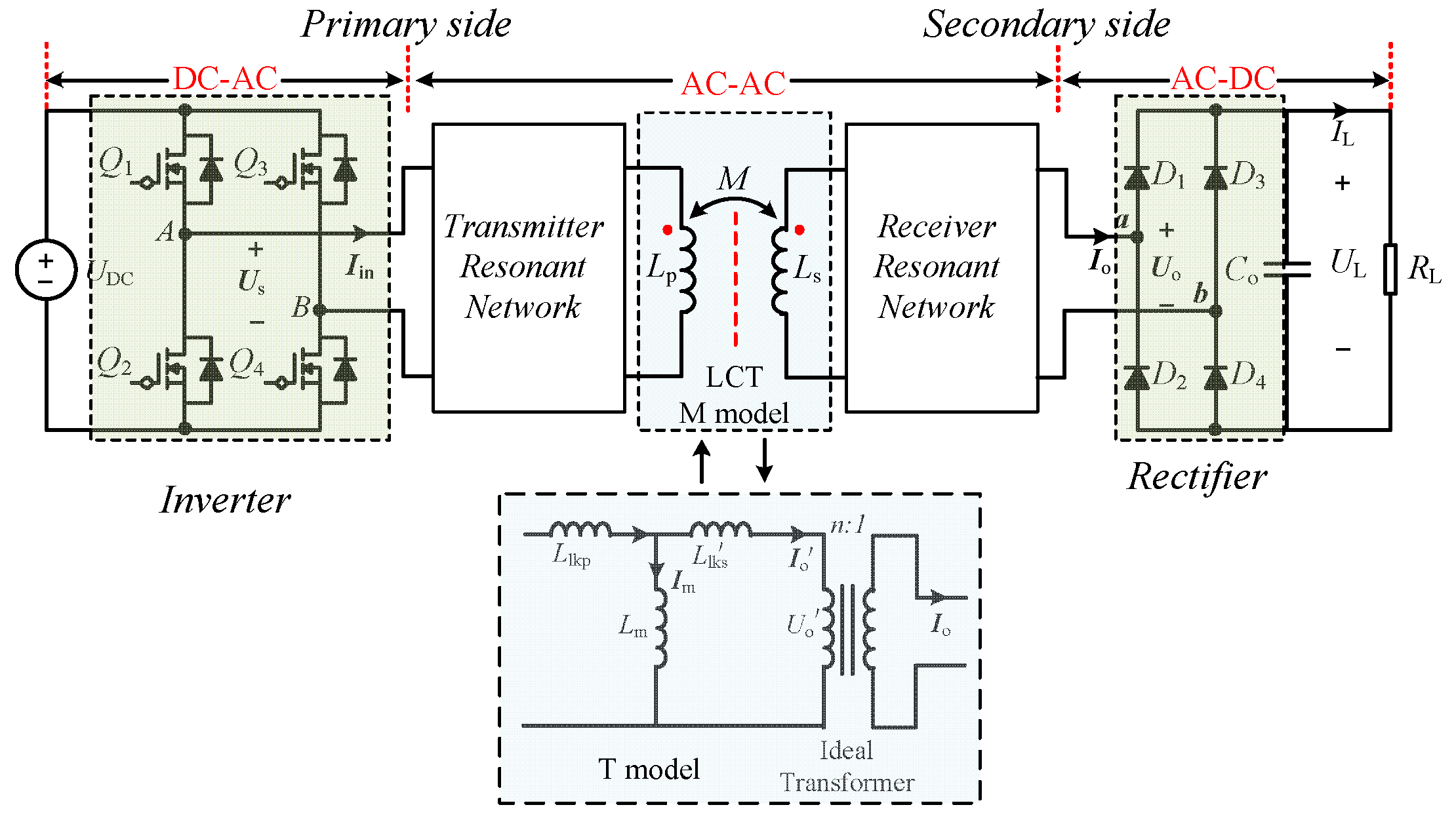
2. Basic Principle
2.1. Fundamentals
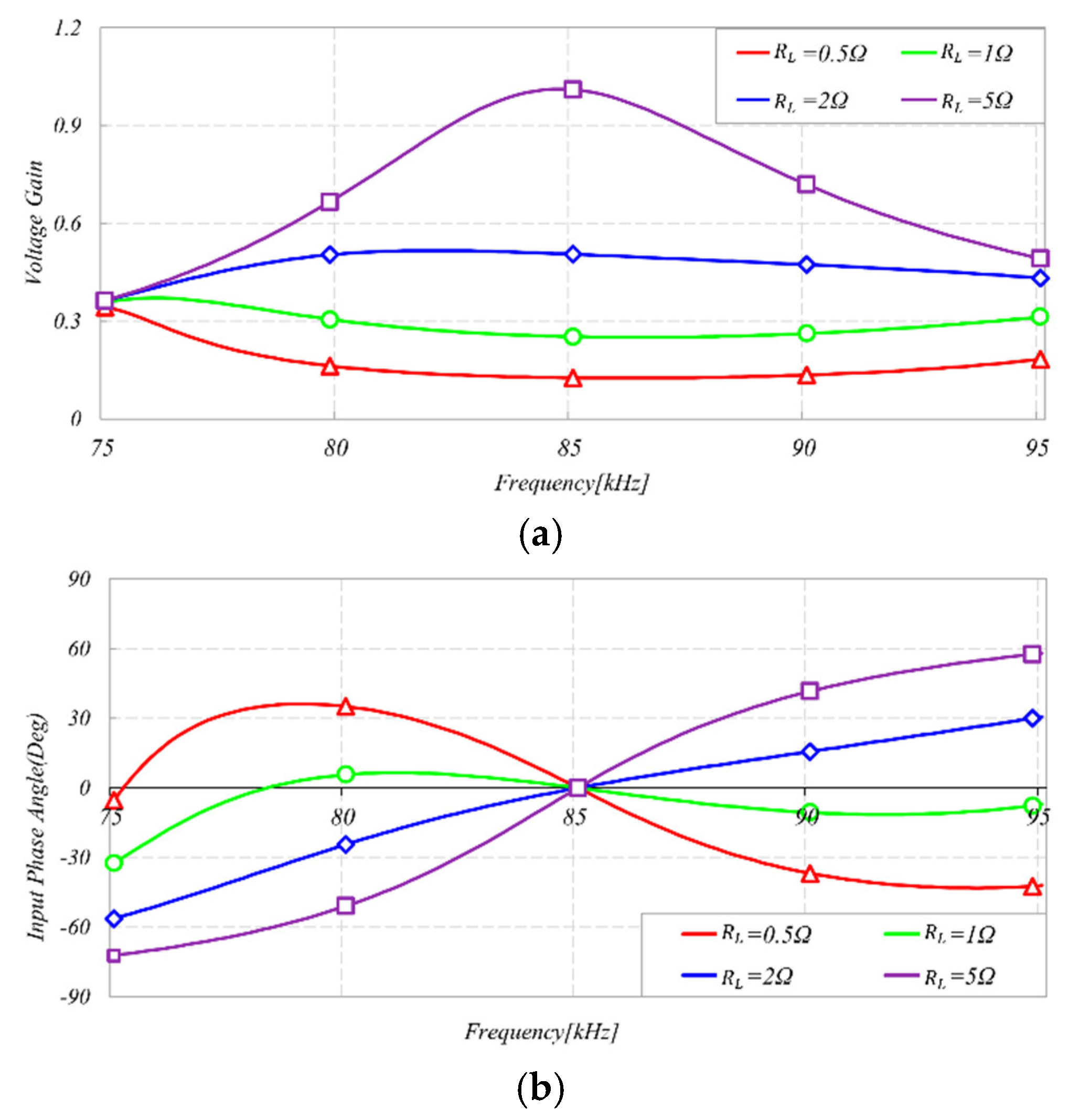
2.2. Basic Analysis of the SS Topology with Conventional Design

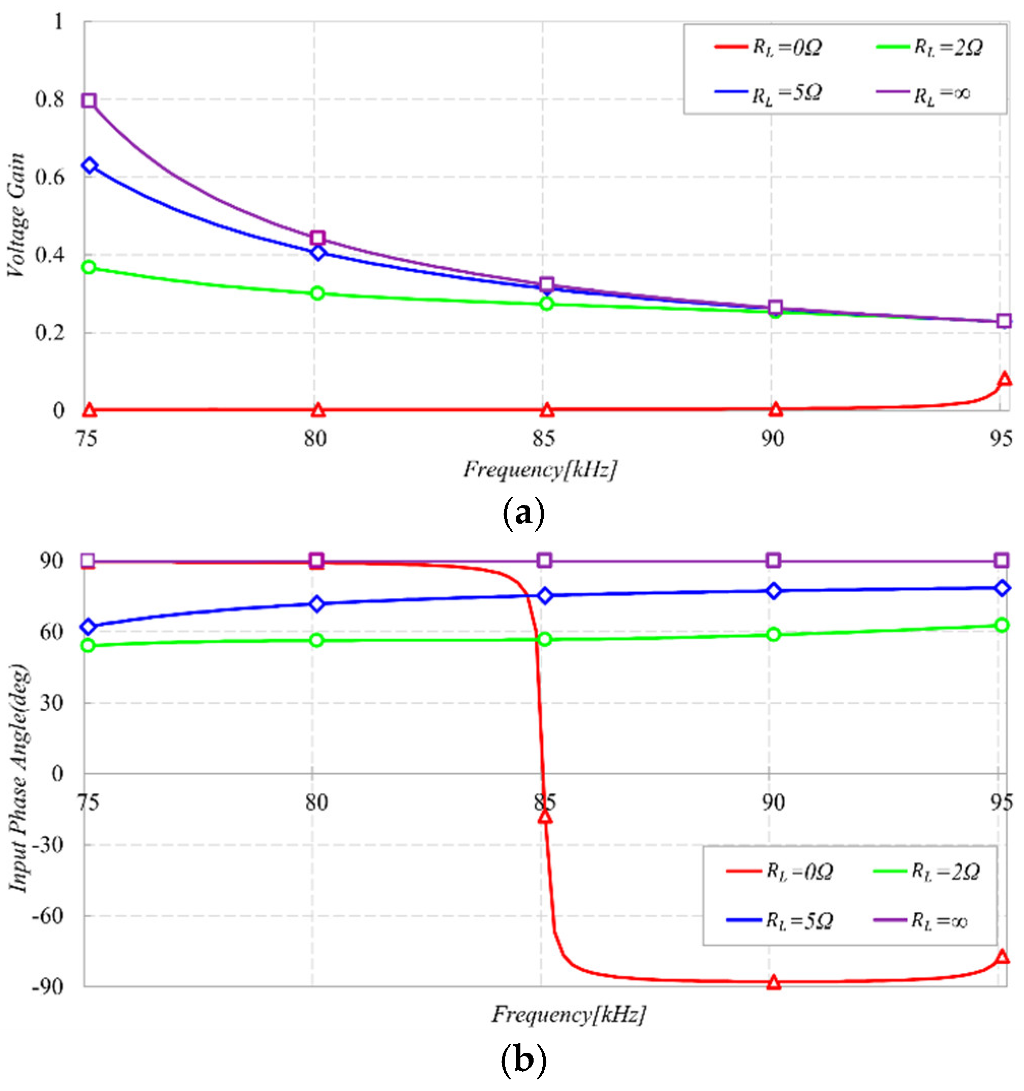
2.3. Basic Analysis of the Proposed Design Method
2.4. Analysis of High Order Harmonic Suppression
3. Analysis of Output Characteristics Variation
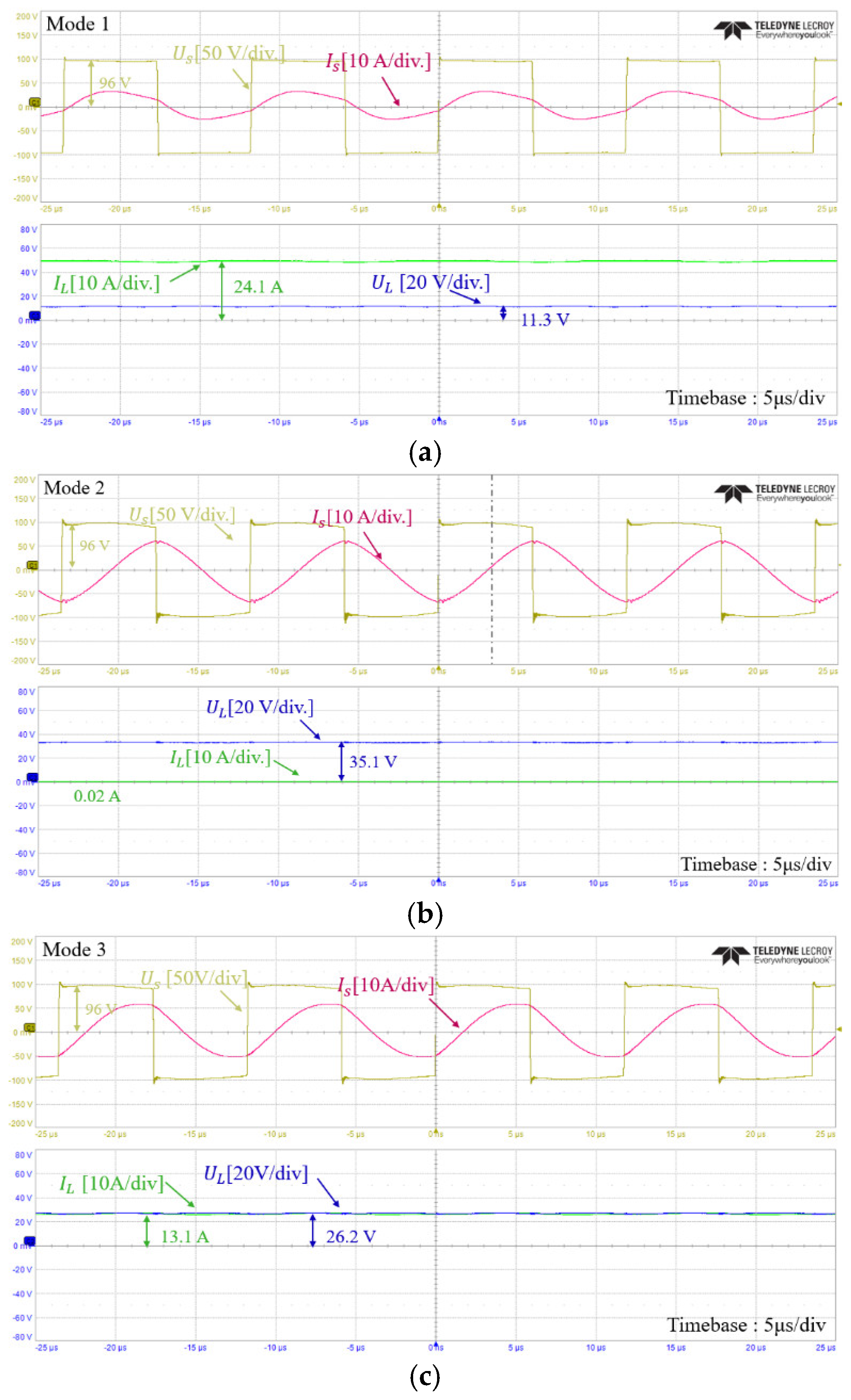
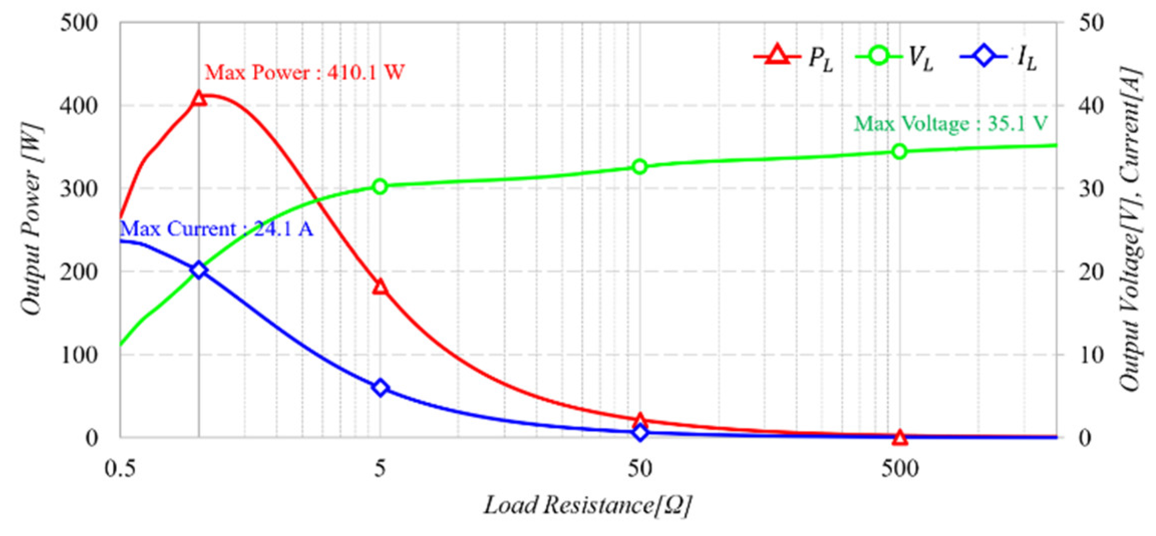
3.1. Mode 1: Current Limitation in Case of Short-Circuit
3.2. Mode 2: Voltage Limitation in Case of an Open-Circuit
3.3. Mode 3: Charging Region
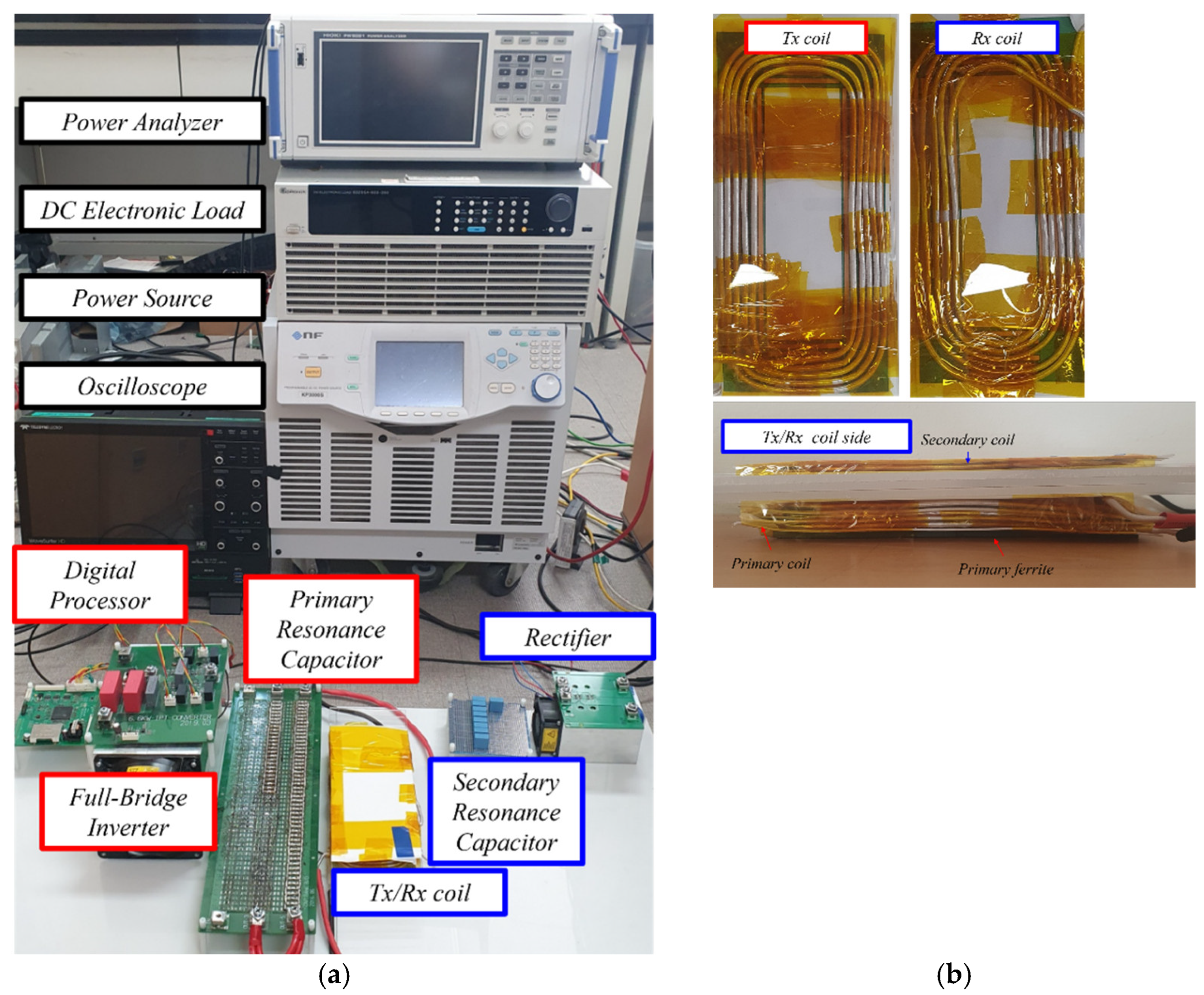
4. Experimental Verification
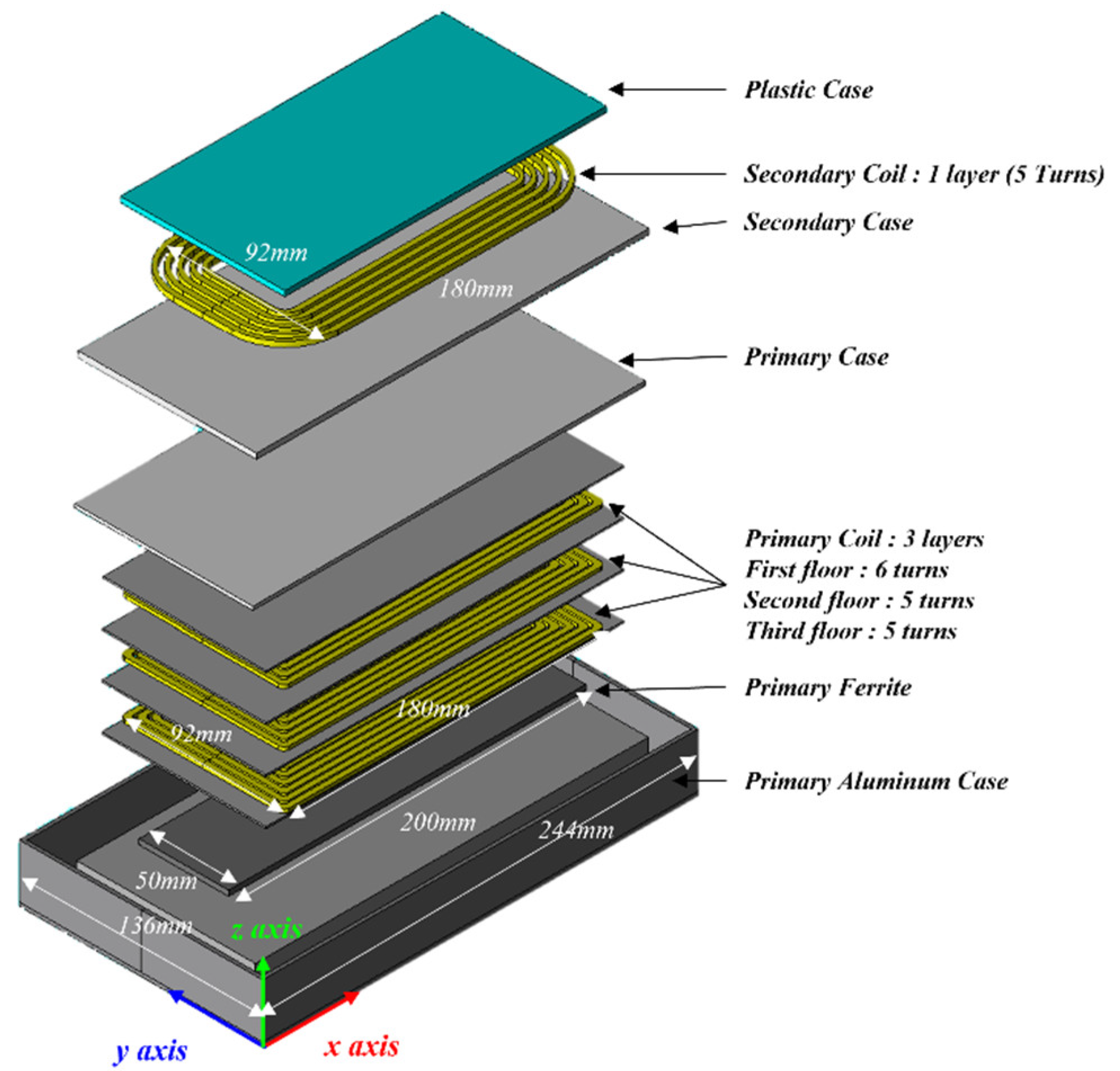
4.1. The Proposed Hybrid IPT Charger’s Parameter Design for CC/CV Modes
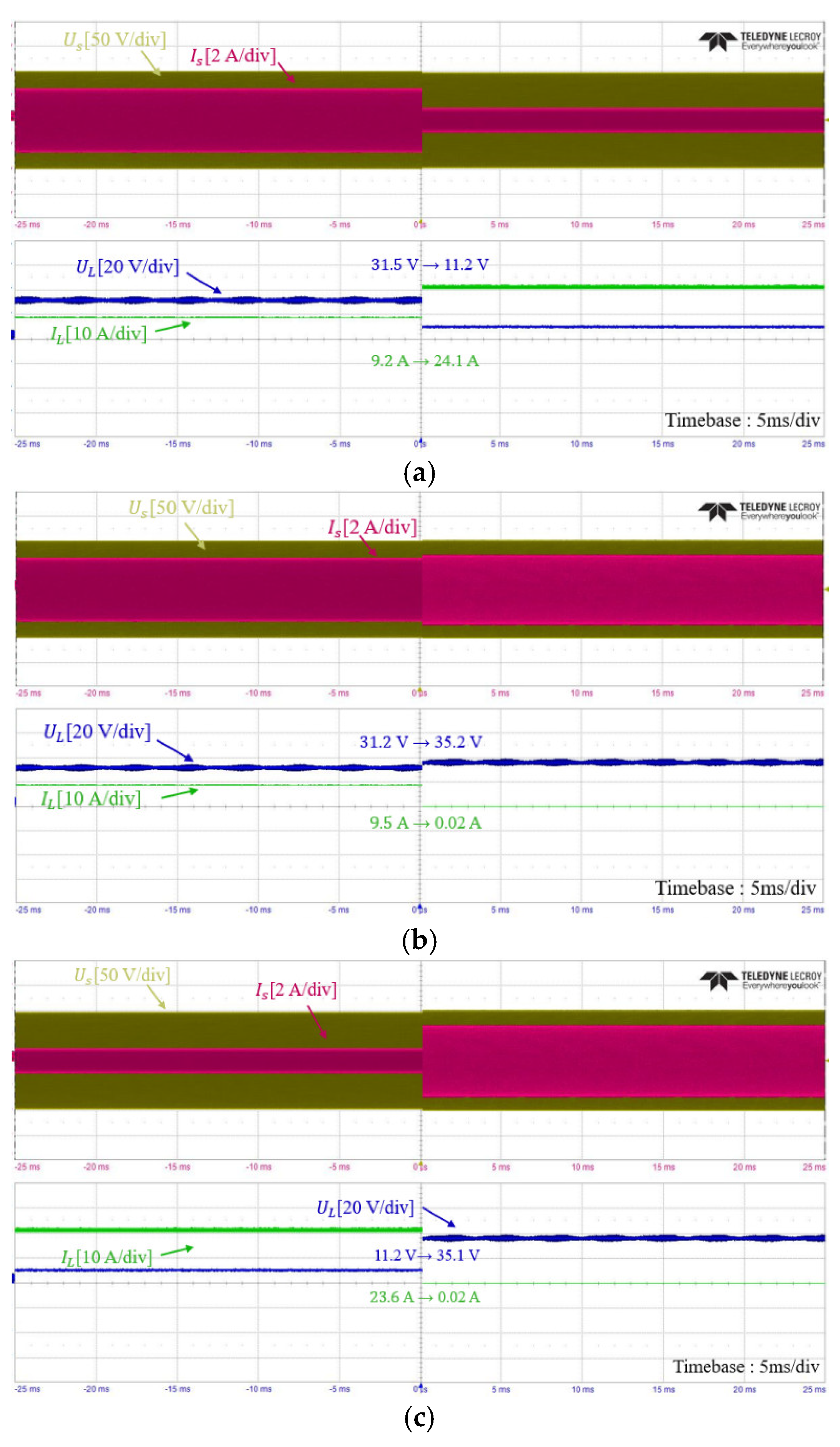
4.2. Experimental Result 1: Verification of Output Characteristic
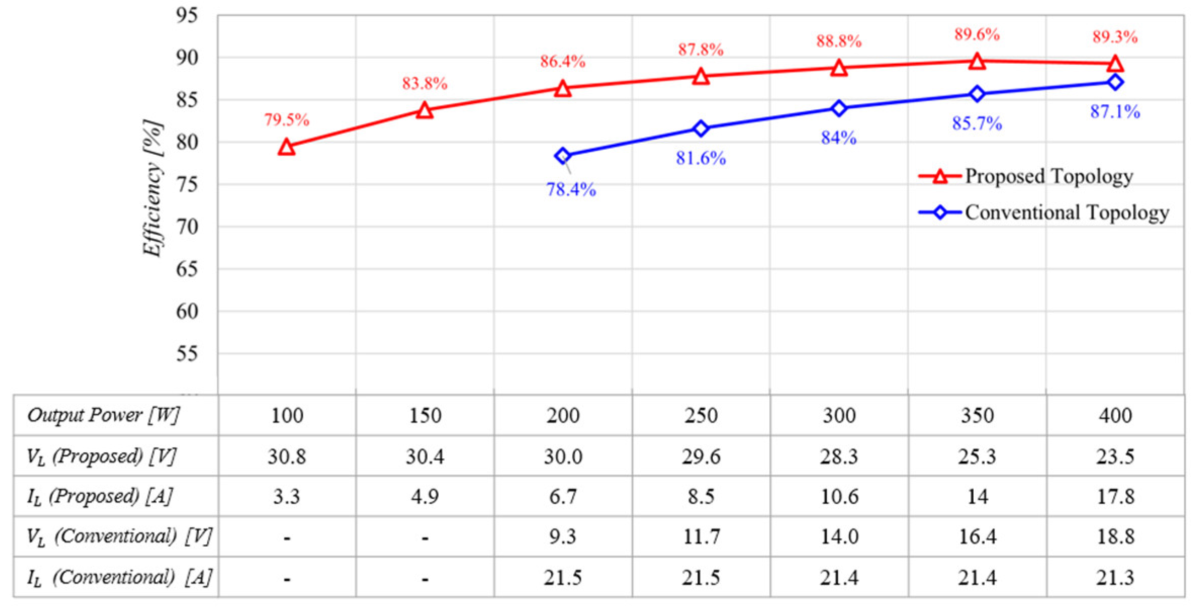
4.3. Experimental Result 2: Comparison of Output Characteristics and Efficiency with the Conventional Design Method
5. Conclusions
Author Contributions
Funding
Institutional Review Board Statement
Informed Consent Statement
Data Availability Statement
Conflicts of Interest
References
- Wang, C.-S.; Stielau, O.H.; Covic, G.A. Design considerations for a contactless electric vehicle battery charger. IEEE Trans. Ind. Electron. 2005, 52, 1308–1314. [Google Scholar] [CrossRef]
- Sample, A.P.; Meyer, D.T.; Smith, J.R. Analysis, experimental results, and range adaptation of magnetically coupled resonators for wireless power transfer. IEEE Trans. Ind. Electron. 2011, 58, 544–554. [Google Scholar] [CrossRef]
- Li, S.; Mi, C.C. Wireless power transfer for electric vehicle applications. IEEE J. Emerg. Sel. Top. Power Electron. 2015, 3, 4–17. [Google Scholar]
- Covic, G.A.; Boys, J.T. Modern trends in inductive power transfer for transportation applications. IEEE J. Emerg. Sel. Top. Power Electron. 2013, 1, 28–41. [Google Scholar] [CrossRef]
- Keskin, N.; Liu, H. Fast charging method for wireless and mobile devices using double-pulse charge technique. In Proceedings of the 2014 IEEE Wireless Power Transfer Conference, Jeju, Republic of Korea, 8–9 May 2014; pp. 44–47. [Google Scholar]
- Sugino, M.; Masamura, T. The wireless power transfer systems using the Class E push-pull inverter for industrial robots. In Proceedings of the 2017 IEEE Wireless Power Transfer Conference, Taipei, Taiwan, 10–12 May 2017; pp. 1–3. [Google Scholar]
- Wang, C.; Ma, Z. Design of wireless power transfer device for UAV. In Proceedings of the 2016 IEEE International Conference on Mechatronics and Automation, Harbin, China, 7–10 August 2016; pp. 2449–2454. [Google Scholar]
- Shanmugam, Y.; Narayanamoorthi, R.; Vishnuram, P.; Bajaj, M.; AboRas, K.M.; Thakur, P. A systematic review of dynamic wireless charging system for electric transportation. IEEE Access 2022, 10, 133617–133642. [Google Scholar] [CrossRef]
- Wang, B.; Dehghanian, P.; Wang, S.; Mitolo, M. Electrical safety considerations in large-scale electric vehicle charging stations. IEEE Trans. Ind. Appl. 2019, 55, 6603–6612. [Google Scholar] [CrossRef]
- Freschi, F.; Mitolo, M.; Tommasini, R. Electrical safety of plug-in electric vehicles: Shielding the public from shock. IEEE Ind. Appl. Mag. 2018, 24, 58–63. [Google Scholar] [CrossRef]
- Cheon, S.; Kim, Y.-H.; Kang, S.-Y.; Lee, M.L.; Lee, J.-M.; Zyung, T. Circuit-model-based analysis of a wireless energy-transfer system via coupled magnetic Resonances. IEEE Trans. Ind. Electron. 2010, 58, 2906–2914. [Google Scholar] [CrossRef]
- Zaheer, A.; Hao, H.; Covic, G.A.; Kacprzak, D. Investigation of multiple decoupled coil primary pad topologies in lumped IPT systems for interoperable electric vehicle charging. IEEE Trans. Power Electron. 2015, 30, 1937–1955. [Google Scholar] [CrossRef]
- Lin, F.Y.; Covic, G.A.; Boys, J.T. Evaluation of magnetic pad sizes and topologies for electric vehicle charging. IEEE Trans. Power Electron. 2015, 30, 6391–6407. [Google Scholar] [CrossRef]
- Nguyen, T.; Li, S.; Li, W.; Mi, C.C. Feasibility study on bipolar pads for efficient wireless power chargers. In Proceedings of the 2014 IEEE Applied Power Electronics Conference and Exposition, Fort Worth, TX, USA, 16–20 March 2014; pp. 1676–1682. [Google Scholar]
- Choi, S.Y.; Huh, J.; Lee, W.Y.; Rim, C.T. Asymmetric coil sets for wireless stationary EV chargers with large lateral tolerance by dominant field analysis. IEEE Trans. Power Electron. 2014, 29, 6406–6420. [Google Scholar] [CrossRef]
- Shevchenko, V.; Husev, O.; Strzelecki, R.; Pakhaliuk, B.; Poliakov, N.; Strzelecka, N. Compensation topologies in IPT systems: Standards, requirements, classification, analysis, comparison and application. IEEE Access 2019, 7, 120559–120580. [Google Scholar] [CrossRef]
- Zhang, W.; Mi, C.C. Compensation topologies of high-power wireless power transfer systems. IEEE Trans. Veh. Technol. 2016, 65, 4768–4778. [Google Scholar] [CrossRef]
- Li, W.; Zhao, H.; Deng, J.; Li, S.; Mi, C.C. Comparison study on SS and double-sided LCC compensation topologies for EV/PHEV wireless chargers. IEEE Trans. Veh. Technol. 2016, 65, 4429–4439. [Google Scholar] [CrossRef]
- Fang, C.; Song, J.; Lin, L.; Wang, Y. Practical considerations of series-series and series-parallel compensation topologies in wireless power transfer system application. In Proceedings of the 2017 IEEE PELS Workshop on Emerging Technologies: Wireless Power Transfer, Chongqing, China, 20–22 May 2017; pp. 255–259. [Google Scholar]
- Yang, B.; Chen, Y.; Ruan, W.; Liu, H.; Ren, Y.; Mai, R. Current stress optimization for double-sided CLLLC topology-based IPT system with constant output current tolerating Pad misalignments. IEEE Trans. Ind. Appl. 2022, 58, 1032–1043. [Google Scholar] [CrossRef]
- Puviwatnangkurn, W.; Tanboonjit, B.; Fuengwarodsakul, N.H. Overcurrent protection scheme of BMS for Li-Ion battery used in electric bicycles. In Proceedings of the 2013 10th International Conference on Electrical Engineering/Electronics, Computer, Telecommunications and Information Technology, Krabi, Thailand, 15–17 May 2013; pp. 1–5. [Google Scholar]
- Salerno, D.; Korsunsky, R. Practical considerations in the design of lithium-ion battery protection systems. In Proceedings of the 1998 Proceedings 13th Annual Applied Power Electronics Conference and Exposition, Anaheim, CA, USA, 15–19 February 1998; Volume 2, pp. 700–707. [Google Scholar]
- Lv, X.; Zhu, Z.; Luo, J.; Wang, X.; Yu, Z. Design method of anti-open protection circuit for MCI-WPT based on SS compensation topology. In Proceedings of the 2019 IEEE 3rd Advanced Information Management, Communicates, Electronic and Automation Control Conference, Chongqing, China, 11–13 October 2019; pp. 900–904. [Google Scholar]
- Chen, Y.; Yang, N.; Liu, L.; Dai, R.; He, Z.; Mai, R. Two/Three-coil hybrid topology for WPT systems charging electric bicycles. In Proceedings of the 2019 IEEE Applied Power Electronics Conference and Exposition, Anaheim, CA, USA, 17–21 March 2019; pp. 3084–3087. [Google Scholar]
- Yan, Z.; Zhang, Y.; Zhang, K.; Song, B.; Li, S.; Kan, T.; Mi, C.C. Fault-tolerant wireless power transfer system with a dual-coupled LCC-S topology. IEEE Trans. Veh. Technol. 2019, 68, 11838–11846. [Google Scholar] [CrossRef]
- Rehman, M.; Nallagownden, P.; Baharudin, Z. Design of a new hybrid topology of WPT system to achieve load-independent constant-current and constant-voltage output. Symmetry 2020, 12, 1453. [Google Scholar] [CrossRef]
- Hwang, S.-H.; Chen, Y.; Zhang, H.; Lee, K.-Y.; Kim, D.-H. Reconfigurable hybrid resonant topology for constant current/voltage wireless power transfer of electric vehicles. Electronics 2020, 9, 1323. [Google Scholar] [CrossRef]
- Yang, J.; Zhang, X.; Yang, X.; Liu, Q.; Sun, Y. A hybrid compensation topology for battery charging system based on IPT technology. Energies 2019, 12, 3818. [Google Scholar] [CrossRef] [Green Version]
- Chen, Y.; Zhang, H.; Park, S.; Kim, D. A Switching hybrid LCC-S compensation topology for constant current/voltage EV Wireless Charging. IEEE Access 2019, 7, 133924–133935. [Google Scholar] [CrossRef]
- Zhang, H.; Chen, Y.; Park, S.; Kim, D. A hybrid compensation topology with single switch for battery charging of inductive power transfer systems. IEEE Access 2019, 7, 171095–171104. [Google Scholar] [CrossRef]
- Steigerwald, R.L. A comparison of half-bridge resonant converter topologies. IEEE Trans. Power Electron. 1988, 3, 174–182. [Google Scholar] [CrossRef]
- Wang, C.-S.; Covic, G.A.; Stielau, O.H. Power transfer capability and bifurcation phenomena of loosely coupled inductive power transfer systems. IEEE Trans. Ind. Electron. 2004, 51, 148–157. [Google Scholar] [CrossRef]
- Chen, Y.; Zhang, H.; Shin, C.; Seo, K.; Park, S.; Kim, D. A comparative study of S-S and LCC-S compensation topology of inductive power transfer systems for EV chargers. In Proceedings of the 2019 IEEE 10th International Symposium on Power Electronics for Distributed Generation Systems, Xi’an, China, 3–6 June 2019; pp. 99–104. [Google Scholar]
- Zeng, H.; Yang, S.; Peng, F.Z. Design consideration and comparison of wireless power transfer via harmonic current. IEEE Trans. Power Electron. 2017, 32, 5943–5952. [Google Scholar] [CrossRef]
- Rahimi-Eichi, H.; Ojha, U.; Baronti, F.; Chow, M.-Y. Battery management system: An overview of its application in the smart grid and electric vehicles. IEEE Ind. Electron. Mag. 2013, 7, 4–16. [Google Scholar] [CrossRef]


| Symbols | Parameters | Values |
|---|---|---|
| Us | DC link voltage | 96 V |
| f | Operation frequency | 85 kHz |
| Po,max | Maximum-output power | 400 W |
| UL | Load voltage range | 0–35.1 V |
| IL,short | Load current under short-circuit | 23.4 A |
| k | Coupling coefficient | 0.324 |
| Lp | Primary self-inductance | 56.76 µH |
| Ls | Secondary self-inductance | 6.628 µH |
| Llk | Primary leakage inductance | 38.421 µH |
| Cr | Leakage resonance capacitor | 91.1 nF |
| RL | Load resistance | 0.46–2000 Ω |
| RLp | AC resistance of Lp | 58.7 mΩ |
| RLs | AC resistance of Ls | 19.2 mΩ |
| Parameters | Values |
|---|---|
| Air gap distance | 10 mm |
| Turns per coil | Np: 17, Ns: 5 |
| Primary coil dimension | 180 mm × 92 mm × 3.1 mm (0.12 mm/500) |
| Primary ferrite plate dimension | 200 mm × 50 mm × 5 mm |
| Primary shield dimension | 244 mm × 136 mm × 2 mm |
| Secondary coil dimension | 180 mm × 92 mm × 3.1 mm (0.12 mm/500) |
| Experimental Outputs | ||||||
|---|---|---|---|---|---|---|
| Pout | Short | 400 | 300 | 200 | 100 | Open |
| VL | Short | 23.46 | 28.25 | 30.01 | 30.81 | 35.1 |
| IL | 24.15 | 17.75 | 10.56 | 6.67 | 3.27 | 0.02 |
| RL | 0.5 | 1.3 | 2.7 | 4.5 | 9.4 | 2000 |
| Symbols | Parameters | Values |
|---|---|---|
| Us | DC link voltage | 96 V |
| IL | Output load current | 21.5 A |
| Cr | Leakage resonance capacitor | 60.4 nF |
| RL | Load resistance | 0.4–0.8 Ω |
Disclaimer/Publisher’s Note: The statements, opinions and data contained in all publications are solely those of the individual author(s) and contributor(s) and not of MDPI and/or the editor(s). MDPI and/or the editor(s) disclaim responsibility for any injury to people or property resulting from any ideas, methods, instructions or products referred to in the content. |
© 2023 by the authors. Licensee MDPI, Basel, Switzerland. This article is an open access article distributed under the terms and conditions of the Creative Commons Attribution (CC BY) license (https://creativecommons.org/licenses/by/4.0/).
Share and Cite
Jo, S.; Shin, C.-S.; Kim, D.-H. Novel Design Method in Wireless Charger for SS Topology with Current/Voltage Self-Limitation Function. Appl. Sci. 2023, 13, 1488. https://doi.org/10.3390/app13031488
Jo S, Shin C-S, Kim D-H. Novel Design Method in Wireless Charger for SS Topology with Current/Voltage Self-Limitation Function. Applied Sciences. 2023; 13(3):1488. https://doi.org/10.3390/app13031488
Chicago/Turabian StyleJo, Seungjin, Chang-Su Shin, and Dong-Hee Kim. 2023. "Novel Design Method in Wireless Charger for SS Topology with Current/Voltage Self-Limitation Function" Applied Sciences 13, no. 3: 1488. https://doi.org/10.3390/app13031488