Abstract
The electron-beam-induced current (EBIC) method is utilized in this work to visualize conductive channels formed in graphene oxide as a result of resistive switching. Using metal–insulator–semiconductor (MIS) structures, an increase in the electron beam induced current by a few orders of magnitude as compared with the EBIC signal in metal–insulator–metal (MIM) structures is achieved. The mechanism of the EBIC image formation related to the conductive channels is explained by the separation and collection of the e-beam generated excess carriers by rectifying barrier nanocontacts formed at the graphene oxide/Si interface during resistive switching. It is shown that the collection efficiency of the formed nanocontacts decreases with the beam energy, in agreement with the theoretical predictions for the Schottky-like nanocontacts. An important advantage of the EBIC method is demonstrated in its ability to monitor the generation and elimination of high density conductive channels even when the current–voltage measurements cannot detect and separate these processes. EBIC study of the dynamics of the conductive channel formation can help better understand the underlying physical mechanisms of their generation.
1. Introduction
The electron-beam-induced current (EBIC) method is a powerful tool for the characterization of electronic devices and analysis of their failure and/or degradation [1,2,3,4]. In semiconductors, EBIC is capable of revealing extended defects, evaluating their recombination activity, and determining excess carrier diffusion length. The interpretation of EBIC data in semiconductor structures with a p/n junction or a Schottky barrier is rather straightforward, as the mechanisms of the EBIC image formation are well understood [3,5,6]. In the work of [7,8], EBIC was successfully used for visualization of the leakage current sites in the gate dielectrics of field effect transistors. However, the EBIC images obtained on the devices with insulating layers can be governed by different and/or additional operative mechanisms, and thus require additional efforts for correct interpretation [7,8,9,10,11]. The frequently observed effect of electron-beam-induced charging in the insulating layers [12,13,14,15,16] makes interpretation of the EBIC images even more difficult.
Recently, owing to a growing interest in the development of insulator-based resistive random access memory (RRAM), the EBIC method was used in several research works to monitor conductive paths in metal-oxide-based structures [11,17,18,19,20,21]. RRAM devices are of significant importance owing to their potential implementation in energy-efficient single-bit memory arrays and/or in multi-bit systems required to create adaptive neuromorphic networks [22,23,24]. However, despite significant progress in the development of resistive memory devices, their practical use is limited by a number of unsolved problems. The most significant problem is a lack of a clear understanding of the operative mechanisms responsible for resistive switching even in metal oxides, such as HfO2, Ta2O5, ZnO, and TiO2, which are the most intensively studied RRAM materials. It is commonly believed that resistive switching in metal oxides is determined by the formation of nanoscale conductive filaments as a result of the motion of oxygen vacancies and/or metal cations [25]. Although several works focused on studying conductive filament formation have been performed using advanced methods such as transmission electron microscopy [26], scanning transmission X-ray microscopy [27], and scalpel scanning probe microscopy [28], a comprehensive picture of the underlying physical mechanism of filament formation has not yet been developed. To explore the origin and dynamics of conductive filament formation in Pt-TiO2-Pt structures, the EBIC method was successfully employed in [11]. By measuring the EBIC current as a function of the beam energy and a special device geometry, the authors attempted to assess the contribution of various competing currents to the measured EBIC signal. As the values of the competing currents in metal–insulator–metal (MIM) structures are of the same order of magnitude as the beam current, it is difficult to unambiguously deconvolute the sources of the measured current and deconstruct a cumulative effect of hot electrons, parasitic leakage, built-in field inversion, and other factors.
Metal–insulator–semiconductor (MIS) structures appear to be more suitable for investigations of resistive switching by EBIC, as the concentration of the excess carriers generated inside a semiconductor substrate is orders of magnitude higher than that of the primary electrons. Therefore, the contribution of the other competing currents to the measured current will be negligible. An additional advantage of MIS structures is an opportunity for quantitative evaluations of both the generation rates and the concentrations of the excess carriers [29]. This assessment is supported by EBIC visualization of leakage current sites in the gate dielectrics of field effect transistors [7,8] and of the conductive paths formed during resistive switching in graphene oxide (GO)-based MIS structures [21]. The EBIC contrast of the conductive path in GO was assumed to be formed as a result of the collection of excess carriers by a conductive path acting as a nanometer size Schottky barrier collector [21]. The possibility to visualize conductive paths in the RRAM insulator materials calls for additional investigation of the mechanism of conductive paths’ image formation in EBIC mode.
The goal of the present work is to study the mechanisms of EBIC imaging of the conductive paths formed in Al-gated graphene-oxide-based MIS structures. Our choice of graphene oxide is motivated by its promising perspectives for non-volatile memory applications [30,31]. Owing to its complex structure, graphene oxide demonstrates multiple transitions from a high to a low resistance state [21,32]. This makes GO a perfect material for investigation of the conductive channels by the EBIC method. Determination of the mechanism of EBIC imaging of the conductive channels can help better understand the mechanism of their formation during resistive switching. The results of the experimental and theoretical study presented in this work have validated an assumption that the mechanism of the conductive path image formation in the Al/GO/Si structures is based on the collection of the excess minority carriers by Schottky-like barrier nanocontacts at the interface with n-type Si. EBIC detection of the minority carrier transport through the insulator to the top electrode provides strong evidence of a close link between the conductive paths and the observed EBIC images.
2. Materials and Methods
The GO-based MIS structures investigated in this work are similar to those used in [21]. GO films with a thickness of 40 nm were synthesized by oxidation of graphite using the modified Hummers’ method [33,34,35] and deposited onto n-type Si substrates (the phosphorus concentration of 1015/cm3) by spin-coating the GO-based sol of 5 mg/mL at a rotation speed of 3000 rpm. The comprehensive characterization of the GO films has been carried out elsewhere [32]. For investigation of the resistive switching characteristics in the GO films, the top electrodes with a diameter of 1 mm were prepared by Al thermal evaporation and the bottom contact was formed by scratching AlGa paste into the rear side of Si. The EBIC study was carried out at room temperature with a scanning electron microscope JSM-840 SEM (Jeol) with a current amplifier Keithley 428. The beam energy Eb was in the range from 10 keV to 35 keV and the beam current was lower than 10−10 A to minimize the irradiation dose during the EBIC imaging. During the EBIC measurements, the Al electrode was grounded and the bias was switched off. The current–voltage (I–V) switching characteristics of the MIS structures placed into the SEM chamber were measured using a Keithley 2450 SourceMeter while an electron beam was turned off. The depth dependence of the e-beam deposited energy was calculated by the Monte Carlo method using an algorithm developed in [36,37] and the GO parameters reported in [38].
3. Results and Discussion
The EBIC image of the virgin graphene-oxide-based MIS structure at zero bias is shown in Figure 1a. The dark and featureless image across the entire contact area can be explained by a high resistance (more than 1 GOhm) of the pristine GO film. The collected current flowing through this highly resistive film is less than 1 nA. After electron beam irradiation at the beam current of 10−10 A for a few tens of minutes, the EBIC images showed no changes, thus indicating a negligible impact on the measured induced current. This is an important feature of the GO film, as it is known that the resistance of the graphene oxide films can be modified during electron beam irradiation [39]. The current–voltage (I–V) characteristics presented in Figure 2 demonstrate the typical switching behavior of GO-based MIS structures. The current–voltage characteristics obtained at both voltage polarities are similar to the earlier observed ones [21,32]. The essential feature of these characteristics is multiple transitions from a high resistance state (HRS) to a low resistance state (LRS) occurring under both polarities of the applied voltage (shown with arrows). After applying a negative voltage to the top electrode (Set step), which resulted in multiple HRS to LRS transitions, the EBIC measurements revealed several bright spots (Figure 1b). Performing Set with a progressively increasing voltage results in an increase in the number of bright spots (Figure 1c). The images of the same area obtained in the secondary electron (SE) mode before and after multiple switching events (Figure 3) clearly indicate that the bright spots are not associated with the appearance of surface defects and/or surface morphology variation. As the current through the MIS structure increased after performing Set with a progressively increased voltage, an increase in the number of bright spots allows to assume their link to the conductive paths formed in GO. During the positive voltage sweep, the GO resistance first smoothly decreased, revealed some tendency to increase at about +5 V, and then continued to decrease, demonstrating several sharp transitions to LRS (Figure 2, magenta curve). The trace-back curve revealed higher current values as compared with the curve obtained during the Set step. Thus, although the Reset process was about to take place, the resulting transition to LRS dominated and the current increased further.
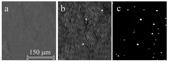
Figure 1.
The EBIC images of the selected region at Eb = 10 keV obtained before (a) and after applying −8 (b) and −15 V (c).
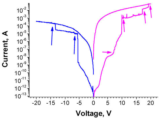
Figure 2.
Typical switching characteristics of Al/GO/n-Si MIS structures showing multiple sharp transitions from HRS to LRS.
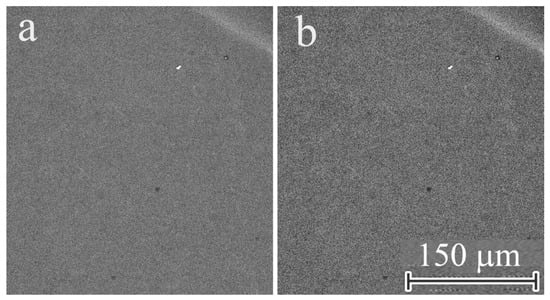
Figure 3.
The secondary electron images of the region shown in Figure 1 before (a) and after applying −15 V (b). The light line in the upper right corner is the edge of the Al contact.
The EBIC images obtained after the Reset step demonstrated that the brightness of some of the conductive channels was notably reduced, while some of the conductive paths completely disappeared. A decreased number of bright spots after a Reset step at 20 V is clearly seen in Figure 4. This provides additional evidence of a direct link between conductive channels formed as a result of resistive switching and the bright spots revealed by EBIC. At the same time, Figure 4 demonstrates the appearance of new conductive channels after Reset, one of which has a very large size and substantially higher brightness. The formation of this additional conductive channel during Reset can explain the resulting increase in the LRS current shown in Figure 2. Thus, it can be concluded that the EBIC method not only is in line with the changes observed in the current–voltage characteristics, but also is able to show that a real scenario of resistive switching in GO is more complex than it can be concluded based on the current–voltage switching characteristics. Thus, it can provide more detailed information on the formation and disappearance of local conductive paths, especially at the Reset step. The difficulty in revealing such behavior from I–V measurements is caused by the cumulative impact of the multiple conductive paths in the GO film under an applied bias, whereas in EBIC mode, each conductive channel contributing to the total current is individually observed.
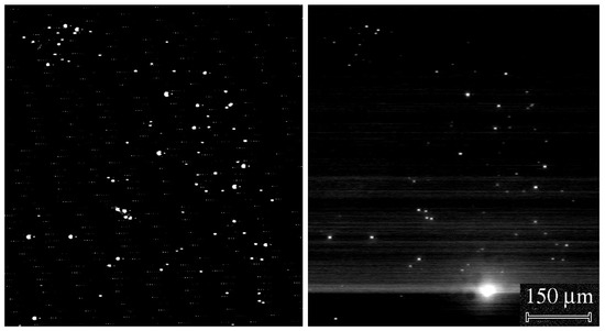
Figure 4.
The EBIC images of the selected region at 10 keV after applying negative bias of 15 V (left) and then positive bias of 20 V (right).
As already pointed out in [11], for probing the underlying physics of the resistive switching mechanism of the conductive path, the EBIC imaging should be elucidated. For this purpose, the dependencies of the EBIC contrast associated with a conductive path on the electron beam energies Eb (from 10 keV to 30 keV) were first investigated. The sign of the contrast was found to be independent of the e-beam energy and corresponds to minority carriers (holes) flowing to the Al top electrode. Analysis of the induced current measured at a typical bright spot at Eb of 10 and 20 keV shows that its values exceed the beam current by 320 and 200 times, respectively. The induced current measured far from the bright spots is about 100 times smaller.
As mentioned above, the induced current consists of a few components. To evaluate the contribution of each of these components to the measured induced current, calculation of the depth dependence of the deposited energy was carried out using the Monte Carlo method. The depth dependencies of the energy deposited by one primary electron with Eb of 10 and 20 keV are shown in Figure 5. According to these results, the energies deposited inside a 40 nm thick GO film are about 185 and 95 eV for 10 and 20 keV electrons, respectively. This implies that, for the GO bandgap of about 3 eV [40,41], each primary electron generates 20 and 10 electron–hole (e–h) pairs, respectively, inside the GO film, as the electron–hole pair creation energy is about three times larger than a bandgap [42]. Thus, even if the excess carrier recombination is neglected, the current induced inside the GO film cannot exceed the beam current by more than 20 times. Owing to recombination, this value should be even lower. This estimation is in agreement with the measurements of the electron-beam-induced current in a thin isolating film, which was of the same order of magnitude as the beam current [43]. The electron emission coefficient from the grounded Al film should be lower than 1, hence the emission current should also be lower than the beam current at the beam energies used. The bright spots in EBIC mode observed in the MIM structures were previously explained by hot carrier injection from the Al electrode [11]. For the MIS structures studied in the present work, the energy deposited in an Al film is 140 and 70 eV for 10 and 20 keV electrons, respectively. Therefore, the number of hot electrons cannot exceed a few tens per one primary electron, especially considering that the escape depth of the hot electrons from Al hardly exceeds a few nm. Therefore, the hot carrier injection from the Al electrode cannot explain the increase in the induced current of a few hundred times. The escape depth of the hot electrons from Si does not exceed 3 nm [44], implying that the number of hot carriers created in this region is not higher than a few carriers per one incident electron. Additionally, such an injection contradicts the direction of the measured current. Based on the above analysis, it can be concluded that the observed local increase in the induced current is caused by the large number of e–h pairs generated inside Si. Indeed, for Eb of 10 and 20 keV, the total number of carriers generated per one incident electron in Si is estimated to be 2270 and 4850, respectively, i.e., high enough to provide the observed current values.
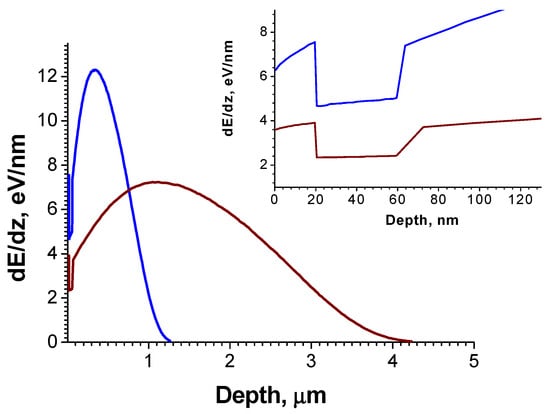
Figure 5.
Deposited energy dependence on depth per one primary electron calculated for Eb of 10 keV (blue) and 20 keV (wine). The inset shows the deposited energy depth dependencies at a small depth.
The formation of the conductive channels results in a local decrease in the GO film resistance. However, in order to contribute to the observed EBIC image at a zero bias, the e–h pairs generated by an electron beam in Si substrate should be separated by a potential barrier at the Si/GO interface. As the experimentally determined sign of the current collected at the bright spots indicates a flow of holes, e–h pairs must be separated by an electric field directed to the structure surface to contribute to the collected current. This implies that the potential barrier should be formed near the GO/Si interface. Formation of this potential barrier can be due to either the existence of a negative charge inside the GO film or the difference in the work function values for n-type Si and graphene oxide. As shown in [21], the presence of a negative charge within the virgin GO film can be ruled out by the capacitance–voltage measurements, revealing the presence of a positive charge that drives n-Si in accumulation. On the other hand, the work function values for GO can vary from 3.7 eV to 5.1 eV [45] and may be larger than that for n-Si (~4.5 eV). Therefore, if the GO properties are locally changed during the process of resistive switching, then a barrier separating generated carriers and collecting holes can be formed owing to the changed GO work function. Although the origin of the hole collecting barrier is not known, we can conclude that this barrier is formed at the interface of the n-Si substrate and the conductive channels are formed within the GO film. This conclusion further confirms the existing link between the bright spots in EBIC mode and the conductive paths in the GO film. The induced current in Si depends on the number of generated excess carriers, which, for the fixed beam current, is proportional to both Eb and the collection probability of the excess carriers. The diffusion length in Si is usually larger than 30–100 μm; therefore, the collection probability should be close to 1 even for Eb = 30 keV. However, the collection probability in the studied structures is notably smaller than 1 and decreases with an increasing Eb. As will be discussed below, this can be considered as an indication of the contact size of the nanometer range.
A decrease in the induced current observed after transition from a high to a low resistance state can be determined by considering a conductive path as a contributor to series resistance for the hole collecting barrier. If the resistance of the conductive path is Rpath, its effect on the measured current Ic can be described as
where I0 is a reverse saturation current flowing through the measured structure, k is Boltzmann constant, T is temperature, n is the ideality factor, and Iind is the current induced by an e-beam inside a semiconductor in the short-circuit condition. It is easy to see from Equation (1) that, under the same excitation conditions, Ic increases with decreasing Rpath, thus allowing to monitor local resistance changes. As an example, the neighboring conductive paths with different brightness are shown in Figure 6. As the SE image in Figure 6b does not reveal any surface defects, which could lead to the contrast difference, a variation in conductive path resistance and/or, as shown below, its radius could be reasons for the different brightness (Figure 6a). The very bright spot shown in Figure 4 is most likely associated with an agglomeration of parallel nano-size conductive paths with a very low combined resistance. Additionally, the bright spots can be revealed only if Rpath is rather low, i.e., only if a conducting channel connects the rectifying contact with the top Al electrode. This provides evidence of the direct link between the bright spots revealed by EBIC and the conductive paths formed during resistive switching.
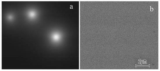
Figure 6.
The EBIC image of conductive paths with different brightness made at Eb = 10 keV (a) and the SE image of the same region (b).
The typical normalized EBIC profiles of the same bright spot measured at Eb of 10, 15, and 20 keV are shown in Figure 7. It is clearly seen that the profile width essentially exceeds the e-beam size (which is about a few tens of nm) and increases with the beam energy. The full width at half maximum (FWHM) calculated based on the data in Figure 7 is equal to 1.2, 1.6, and 2.2 μm for 10, 15, and 20 keV, respectively. At Eb larger than 20 keV, the FWHM values do not increase further, but even show a tendency to decrease (Figure 8). As mentioned above, the number of carriers contributing to the induced current at a bright spot is 320 and 200 per one primary electron for 10 and 20 keV, respectively, while the total number of generated carriers at 20 keV is two times higher than that for 10 kV. This implies that the collection efficiency at 20 keV is about three times lower than that at 10 keV, and thus is in agreement with the theoretical predictions for the rectifying nanocontact [46,47], showing that the collection probability strongly decreases with the distance from the contact. This allows to explain the observed FWHM dependence on Eb. The width of the generation volume at z < R is roughly proportional to (z3/R)1/2, where z is the depth and R ~ Eb1.75 is the electron range [48]. Thus, while dimensions of the generation region are roughly proportional to R and increase with Eb, the width of a part of the generated volume adjusting the contact decreases with Eb. Besides, the penetration depth of the electrons increases with Eb, while the collection probability of the excess carriers strongly decreases for nanosize contacts. Therefore, a relative portion of the carriers generated in the vicinity of the top electrode, and thus contributing to the EBIC signal, increase with the increasing Eb. Competition of these factors explains the non-monotonic dependence presented in Figure 8. Thus, the observed Eb dependence of the bright spot width supports an assumption of the formation of a nanosize rectifying barrier at the conductive path/Si interface. It should be noted that, for the rectifying contact, the depletion region width, which plays the role of the collector for the minority carriers (holes), can vary from a few hundreds to several thousands of nanometers depending on the barrier height and the dopant concentration [49]. It should be emphasized that the real size of the conductive channels can essentially be smaller.
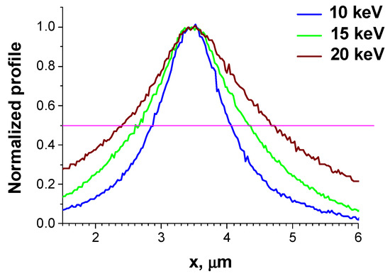
Figure 7.
Profiles of the EBIC image of the same bright spot measured at a few Eb values. A solid line marks the half maximum position.
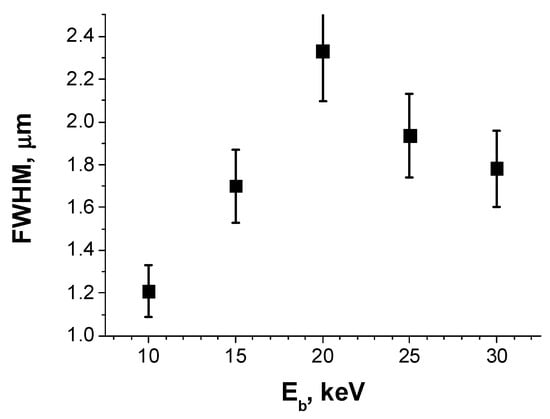
Figure 8.
Dependence of FWHM of the conductive channel EBIC profile on Eb.
4. Conclusions
This work has demonstrated the strong potential of EBIC for visualization of the conductive paths formed in graphene oxide as a result of resistive switching. It is shown that the EBIC method is capable of revealing both the generation and elimination of multiple conductive channels, while these processes cannot be detected by I–V measurements. The EBIC study can provide additional information on the individual conductive channel resistance and stability, thus helping better understand the mechanisms of resistive switching in graphene oxide and other insulators with resistive switching properties. Evaluation of the current components contributing to the induced current confirmed the dominating role of the Si substrate. Formation of the rectifying contacts implies that the conductive path formation leads to an increase in work function, or that the conductive paths contain negatively charged traps. As the EBIC signals reflecting the formation of the conductive paths can be observed at zero bias, it is concluded that the conductive paths formed during resistive switching in graphene oxide play a dual role; that is, they form rectifying nanocontacts at the graphene oxide/Si interface and connect them with the top Al electrode. The collection efficiency of these nanocontacts decreases with the beam energy, which is in good agreement with the theoretical predictions for the behavior of the Schottky nanocontact. The concentration of the generated excess carriers is found to be orders of magnitude higher than that of the primary electrons, thus providing the strong advantage of EBIC sensitivity for metal–insulator–semiconductor devices as compared with metal–insulator–metal structures. EBIC studies using a similar analysis can provide valuable information about the mechanisms of the formation and nature of conductive paths formed as a result of resistive switching in other oxide materials.
Author Contributions
Conceptualization, E.B.Y. and S.K.; methodology, E.B.Y., S.K. and O.K.; investigation, E.B.Y., S.K. and O.K.; writing—original draft preparation, E.B.Y. and O.K.; writing—review and editing, E.B.Y. and S.K. All authors have read and agreed to the published version of the manuscript.
Funding
This research was carried out within the framework of the State Task No 075-01304-23-00.
Institutional Review Board Statement
Not applicable.
Informed Consent Statement
Not applicable.
Data Availability Statement
Data are contained within the article.
Conflicts of Interest
The authors declare no conflict of interest.
References
- Hanoka, J.I.; Bell, R.O. Electron-Beam-Induced Currents in Semiconductors. Ann. Rev. Mater. Sci. 1981, 11, 353–380. [Google Scholar] [CrossRef]
- Leamy, H.J. Charge collection scanning electron microscopy. J. Appl. Phys. 1982, 53, R51–R80. [Google Scholar] [CrossRef]
- Yakimov, E.B. Electron-beam-induced-current study of defects in GaN; Experiments and simulation. J. Phys. Condens. Matter. 2002, 14, 13069–13077. [Google Scholar] [CrossRef]
- Yakimov, E.B. Study of Wide-Gap Semiconductors Using Electron-Beam Induced Current Method. Crystallogr. Rep. 2021, 66, 581–593. [Google Scholar] [CrossRef]
- Donolato, C. Theory of beam induced current characterization of grain boundaries in polycrystalline solar cells. J. Appl. Phys. 1983, 54, 1314–1322. [Google Scholar] [CrossRef]
- Donolato, C. Modeling the effect of dislocations on the minority carrier diffusion length of a semiconductor. J. Appl. Phys. 1998, 84, 2656–2664. [Google Scholar] [CrossRef]
- Chen, J.; Sekiguchi, T.; Fukata, N.; Takase, M.; Chikyow, T.; Yamabe, K.; Hasunuma, R.; Akasaka, Y.; Inumiya, S.; Nara, Y.; et al. Observation of leakage sites in a hafnium silicon oxynitride gate dielectric of a metal-oxide-semiconductor field-effect transistor device by electron-beam-induced current. Appl. Phys. Lett. 2006, 89, 222104. [Google Scholar] [CrossRef]
- Chen, J.; Sekiguchi, T.; Fukata, N.; Takase, M.; Nemoto, Y.; Hasunuma, R.; Yamabe, K.; Sato, M.; Yamada, K.; Chikyow, T. An Electron-Beam-Induced Current Investigation of Electrical Defects in High-k Gate Stacks. ECS Trans. 2010, 28, 299–313. [Google Scholar] [CrossRef]
- Aris, F.C.; Davies, P.M.; Lewis, T.J. Electron-beam-induced conduction in dielectrics. J. Phys. C Solid State Phys. 1976, 9, 797–808. [Google Scholar] [CrossRef]
- Nakamae, K.; Fujioka, H.; Ura, K. Electron-beam-induced current in a chemical-vapour-deposited SiO2 passivation layer on an MOS structure with a non-penetrating electron beam. J. Phys. D Appl. Phys. 1991, 24, 963–968. [Google Scholar] [CrossRef]
- Hoskins, B.D.; Adam, G.C.; Strelcov, E.; Zhitenev, N.; Kolmakov, A.; Strukov, D.B.; McClelland, J.J. Stateful characterization of resistive switching TiO2 with electron beam induced currents. Nat. Commun. 2017, 8, 1972. [Google Scholar] [CrossRef] [PubMed]
- Belhaj, M.; Jbara, O.; Filippov, M.N.; Rau, E.I.; Andrianov, M.V. Analysis of two methods of measurements of surface potential of insulators in SEM: Electron spectroscopy and X-ray spectroscopy methods. Appl. Surf. Sci. 2001, 177, 58–65. [Google Scholar] [CrossRef]
- Zhang, H.-B.; Feng, R.-J.; Ura, K. Utilizing the charging effect in scanning electron microscopy. Sci. Prog. 2004, 87, 249–268. [Google Scholar] [CrossRef] [PubMed]
- Vergeles, P.S.; Kulanchikov, Y.O.; Yakimov, E.B. Charging Effects in Al-SiO2-p-Si Structures After Low-Energy Electron Beam Irradiation. J. Electron. Mater. 2020, 49, 5178–5183. [Google Scholar] [CrossRef]
- Ding, Z.J.; Li, C.; Da, B.; Liu, J. Charging effect induced by electron beam irradiation: A review. Sci. Technol. Adv. Mater. 2021, 22, 932–971. [Google Scholar] [CrossRef]
- Rau, E.I.; Tatarintsev, A.A. Modification of the model of charging dielectrics under electron beam irradiation. J. Appl. Phys. 2022, 132, 184102. [Google Scholar] [CrossRef]
- Rossel, C.; Meijer, G.I.; Brémaud, D.; Widmer, D. Electrical current distribution across a metal–insulator–metal structure during bistable switching. J. Appl. Phys. 2001, 90, 2892–2898. [Google Scholar] [CrossRef]
- Regan, B.C.; Lodico, J.; Hubbard, W.A. Scanning TEM EBIC Imaging of Resistive Memory Switching Processes. Microsc. Microanal. 2018, 24 (Suppl. S1), 1806–1807. [Google Scholar] [CrossRef]
- Sun, W.; Gao, B.; Chi, M.; Xia, Q.; Yang, J.J.; Qian, H.; Wu, H. Understanding memristive switching via in situ characterization and device modeling. Nat. Commun. 2019, 10, 3453. [Google Scholar] [CrossRef]
- Yi, W.; Chen, J.; Sekiguchi, T. Electron-Beam-Induced Current and Cathodoluminescence Study of Dislocations in SrTiO3. Crystals 2020, 10, 736. [Google Scholar] [CrossRef]
- Koveshnikov, S.; Kononenko, O.; Soltanovich, O.; Kapitanova, O.; Knyazev, M.; Volkov, V.; Yakimov, E. Multiple Resistive Switching Mechanisms in Graphene Oxide-Based Resistive Memory Devices. Nanomaterials 2022, 12, 3626. [Google Scholar] [CrossRef]
- Wu, H.; Wang, X.H.; Gao, B.; Deng, N.; Lu, Z.; Haukness, B.; Bronner, G.; Qian, H. Resistive Random Access Memory for Future Information Processing System. Proc. IEEE 2017, 105, 1770–1789. [Google Scholar] [CrossRef]
- Hong, H.; Loy, D.J.; Dananjaya, P.A.; Tan, F.; Ng, C.; Lew, W. Oxide-based RRAM materials for neuromorphic computing. J. Mater. Sci. 2018, 53, 8720–8746. [Google Scholar] [CrossRef]
- Cai, F.; Yen, S.-H.; Uppala, A.; Thomas, L.; Liu, T.; Fu, P.; Zhang, X.; Low, A.; Kamalanathan, D.; Hsu, J.; et al. A Fully Integrated System-on-Chip Design with Scalable Resistive Random-Access Memory Tile Design for Analog in-Memory Computing. Advanc. Intellig. Syst. 2022, 4, 2200014. [Google Scholar] [CrossRef]
- Waser, R.; Aono, M. Nanoionics-based resistive switching memories. Nat. Mater. 2007, 6, 833–840. [Google Scholar] [CrossRef]
- Kwon, J.; Sharma, A.; Chen, C.-Y.; Fantini, A.; Jurczak, M.; Herzing, A.; Bain, J.; Picard, Y.; Skowronski, M. Transient thermometry and high resolution transmission electron microscopy analysis of filamentary resistive switchers. ACS Appl. Mater. Interfaces 2016, 8, 20176–20184. [Google Scholar] [CrossRef] [PubMed]
- Kumar, S.; Graves, C.; Strachan, J.; Grafals, E.; Kilcoyne, A.; Tyliszczak, T.; Weker, J.; Nishi, Y.; Williams, S. Direct observation of localized radial oxygen migration in functioning tantalum oxide memristors. Adv. Mater. 2016, 28, 2772–2776. [Google Scholar] [CrossRef]
- Celano, U.; Goux, L.; Degraeve, R.; Fantini, A.; Richard, O.; Bender, H.; Jurczak, M.; Vandervorst, W. Imaging the three-dimensional conductive channel in filamentary-based oxide resistive switching memory. Nano Lett. 2015, 15, 7970–7975. [Google Scholar] [CrossRef]
- Yakimov, E.B. Electron beam induced excess carrier concentration. Phys. Status Solidi C 2017, 14, 1600266. [Google Scholar] [CrossRef]
- Porro, S.; Accornero, E.; Pirri, C.F.; Ricciardi, C. Memristive devices based on graphene oxide. Carbon 2015, 85, 383–396. [Google Scholar] [CrossRef]
- Romero, F.J.; Toral, A.; Medina-Rull, A.; Moraila-Martinez, C.L.; Morales, D.P.; Ohata, A.; Godoy, A.; Ruiz, F.G.; Rodriguez, N. Resistive Switching in Graphene Oxide. Front. Mater. 2020, 7, 17. [Google Scholar] [CrossRef]
- Brzhezinskaya, M.; Kapitanova, O.O.; Kononenko, O.V.; Koveshnikov, S.; Korepanov, V.; Roshchupkin, D. Large-scalable graphene oxide films with resistive switching for nonvolatile memory applications. J. Alloys Compd. 2020, 849, 156699. [Google Scholar] [CrossRef]
- Marcano, D.C.; Kosynkin, D.V.; Berlin, J.M.; Sinitskii, A.; Sun, Z.; Slesarev, A.; Alemany, L.B.; Lu, W.; Tour, J.M. Improve synthesis of graphene oxide. ACS Nano 2010, 4, 4806–4814. [Google Scholar] [CrossRef] [PubMed]
- Panin, G.N.; Kapitanova, O.O.; Lee, S.W.; Baranov, A.N.; Kang, T.W. Resistive switching in Al/graphene oxide/Al structure. Jpn. J. Appl. Phys. 2011, 50, 070110. [Google Scholar] [CrossRef]
- Rasheed, M.; Shihab, S.; Sabah, O.W. An investigation of the Structural, Electrical and Optical Properties of Graphene-Oxide Thin Films Using Different Solvents. J. Phys. Confer. Ser. 2021, 1795, 012052. [Google Scholar] [CrossRef]
- Zaitsev, S.I.; Pavlov, V.N.; Panchenko, V.Y.; Polikarpov, M.A.; Svintsov, A.A.; Yakimov, E.B. Comparison of the Efficiency of 63Ni Beta_Radiation Detectors Made from Silicon and Wide-Gap Semiconductors. J. Surf. Investig. 2014, 8, 843–845. [Google Scholar] [CrossRef]
- Svintsov, A.A.; Knyazev, M.A.; Zaitsev, S.I. Calculation of the Absorbed Electron Energy 3D Distribution by the Monte Carlo Method, Presentation of the Proximity Function by Three Parameters α, β, η and Comparison with the Experiment. Materials 2022, 15, 3888. [Google Scholar] [CrossRef] [PubMed]
- Torrisi, L.; Cutroneo, M.; Torrisi, A.; Silipigni, L. Measurements on Five Characterizing Properties of Graphene Oxide and Reduced Graphene Oxide Foils. Phys. Status Solidi A 2022, 219, 2100628. [Google Scholar] [CrossRef]
- Tyagi, C.; Lakshmi, G.B.V.S.; Kumar, S.; Tripathi, A.; Avasthi, D.K. Structural changes in graphene oxide thin film by electron-beam irradiation. Nuclear Instrum. Methods Phys. Res. B 2016, 379, 171–175. [Google Scholar] [CrossRef]
- de Lima, A.H.; Tavares, C.T.; da Cunha, C.C.S.; Vicentini, N.C.; Carvalho, G.R.; Fragneaud, B.; Maciel1, I.O.; Legnani, C.; Quirino, W.G.; de Oliveira, L.F.C.; et al. Origin of optical bandgap fluctuations in graphene oxide. Eur. Phys. J. B 2020, 93, 105. [Google Scholar] [CrossRef]
- Sharma, N.; Arif, M.; Monga, S.; Shkir, M.; Mishra, Y.K.; Singh, A. Investigation of bandgap alteration in graphene oxide with different reduction routes. Appl. Surface Sci. 2020, 513, 145396. [Google Scholar] [CrossRef]
- Yakimov, E.B.; Polyakov, A.Y.; Shchemerov, I.V.; Smirnov, N.B.; Vasilev, A.A.; Vergeles, P.S.; Yakimov, E.E.; Chernykh, A.V.; Ren, F.; Pearton, S.J. Experimental estimation of electron–hole pair creation energy in β-Ga2O3. Appl. Phys. Lett. 2021, 118, 202106. [Google Scholar] [CrossRef]
- Borisov, S.S.; Vergeles, P.S.; Yakimov, E.B. Investigations of Electron Beam Induced Conductivity in Silicon Oxide Thin Films. J. Surf. Investig. 2010, 4, 754–757. [Google Scholar] [CrossRef]
- Lin, Y.; Joy, D.C. A new examination of secondary electron yield data. Surf. Interface Anal. 2005, 37, 895–900. [Google Scholar] [CrossRef]
- Ji, S.; Min, B.K.; Kim, S.K.; Myung, S.; Kang, M.; Shin, H.-S.; Song, W.; Heo, J.; Lim, J.; An, K.-S.; et al. Work function engineering of grapheme oxide via covalent functionalization for organic field-effect transistors. Appl. Surf. Sci. 2017, 419, 252–258. [Google Scholar] [CrossRef]
- Ledra, M.; Tabet, N. Monte Carlo simulation of the EBIC collection efficiency of a Schottky nanocontact. Superlatt. Microstruct. 2009, 45, 444–450. [Google Scholar] [CrossRef]
- Doan, Q.T.; El Hdiy, A.; Troyon, M. Three-dimensional simulation of electron beam induced current collected by a nano-contact: Diffusion and collection analysis. J. Appl. Phys. 2011, 110, 124515. [Google Scholar] [CrossRef]
- Donolato, C. An Analytical Model of SEM and STEM Charge Collection Images of Dislocations in Thin Semiconductor Layers I. Minority Carrier Generation, Diffusion, and Collection. Phys. Status Solidi A 1981, 65, 649–658. [Google Scholar] [CrossRef]
- Donolato, C. Approximate analytical solution to the space charge problem in nanosized Schottky diodes. J. Appl. Phys. 2004, 95, 2184–2186. [Google Scholar] [CrossRef]


Disclaimer/Publisher’s Note: The statements, opinions and data contained in all publications are solely those of the individual author(s) and contributor(s) and not of MDPI and/or the editor(s). MDPI and/or the editor(s) disclaim responsibility for any injury to people or property resulting from any ideas, methods, instructions or products referred to in the content. |
© 2023 by the authors. Licensee MDPI, Basel, Switzerland. This article is an open access article distributed under the terms and conditions of the Creative Commons Attribution (CC BY) license (https://creativecommons.org/licenses/by/4.0/).