Article

A Method of Extracting Transmission Characteristics of Interconnects from Near-Field Emissions in PCBs

1
The School of Electronic and Information Engineering, Beihang University, Beijing 100191, China
2
The Research Institute for Frontier Science, Beihang University, Beijing 100191, China
*
Author to whom correspondence should be addressed.
Appl. Sci. 2023, 13(5), 2874; https://doi.org/10.3390/app13052874
Submission received: 23 January 2023 / Revised: 20 February 2023 / Accepted: 21 February 2023 / Published: 23 February 2023

Abstract

:
This paper proposes a method for extracting transmission characteristics of interconnects in printed circuit boards (PCBs) from near-field emission. A wideband microstrip line electric probe is used to measure the near-field emission. There are two key technologies in the extraction principle, obtaining the transfer function and the input signal estimation, and they are explained in detail. To validate the method, one-trace structures, including a corner trace and a via trace, and a multi-trace structure were measured. The transmission characteristics extracted by the proposed method agrees well with the standard vector network analyzer (VNA) measurements up to frequency of 12 GHz. The error caused by the distance and the disturbance signal is investigated.

1. Introduction

Near-field measurements have been widely used in electromagnetic compatibility (EMC) applications, especially in the electromagnetic interference (EMI) detection of large-scale integrated circuits (ICs) and the EMI source location of high-speed printed circuit boards (PCBs) [1], etc. Meanwhile, the transmission characteristics of interconnects are receiving a lot of attention in high-speed and fast-switching PCBs. Interconnect-induced emissions and signal quality degradations become increasingly difficult to be ignored as the transmission and switching speeds increase. It is convenient and efficient to detect the transmission characteristics from near-field emissions in order to diagnose abnormal functionalities and achieve a good signal quality along the traces.
For near-field emission characteristics extraction, the commonly accepted method is interference sources identification [2,3,4,5]. However, electromagnetic emission is an inherent property of the product, which is determined by the interference sources and peripheral circuits [2]. For example, the ring generated by the mismatch can cause the spectrum to rise at a particular frequency [6]. In it, a method for extracting the mismatch characteristics from a conducted emission spectrum was proposed using particle swarm optimization (PSO). A method for extracting the noise source impedance of switched-mode power supplies (SMPS) during operational conditions was presented [7]. The impedance can be used to model the equivalent circuit of the conducted emission with the interference sources. The authors of [8] extracted the transmission characteristics of peripheral circuits from digital circuit-induced emissions based on the autocorrelation function, but the transmission characteristics are not physical. The methods noted above are all used for the conducted analysis, and we mainly focus on frequencies lower than 1 GHz.
For other noncontact measurements, there are mainly two approaches that have been reported. The first one measures the surface electric and magnetic field distributions of the circuits using near-field probes. This technique can be used for a performance and failure analysis in microwave circuits [9,10,11]. One measures the S-parameters of the traces using capacitive or inductive probes, in which the calculation of the propagating waves is achieved by using two probes separated by a certain distance or a single probe moved to two locations [12,13,14]. In addition, a probe was used to measure the current and voltage on a trace; an algorithm was also used based on the transfer functions to quantify the capacitive and inductive couplings between the probe and the trace during the test [15,16,17]. Meanwhile, most studies on interconnects have concentrated on the characteristics calculation. The authors of [18,19,20] proposed methods that can contribute to fast analysis, which are based on the physics-based via and trace models. The method in [21] combined a systematic analysis with an evaluation of energy efficiency to find improved off-chip interconnect design solutions, while the authors of [22] used artificial neural networks (ANNs) as a surrogate model to optimize the energy-efficient on-chip interconnect.
In this study, we present a new measurement and analysis method for extracting the transmission characteristics of interconnects from near-field emissions in PCBs. By adopting using a wideband microstrip line electric probe, near-field emissions are captured. By applying the transfer function between the printed traces being tested and the probe and the reconstructed input signal waveforms, the transmission characteristics can be extracted from the emission. The transfer function is modeled using equivalent circuits, which is validated by full wave simulation and an experiment. The algorithm is programmed based on the autocorrelation function, adaptive wind-driven optimization (AWDO), and Fast Fourier transformation (FFT). To validate the method, the transmission characteristics of one-trace and multi-trace structures are measured, analyzed, and compared to those obtained by VNA directly. Considering the mobility of the probe, the measurement accuracy caused by spatial and perturbance errors are also investigated.
The rest of the paper is structured as follows: Section 2 describes the theories of an electric probe for electric field coupling and the computation of transmission characteristics extraction. Subsequently, Section 3 introduces the procedures of transfer function modeling and algorithm programming. Next, Section 4 illustrates the validation of the approach using typical structures, including a printed trace with a via hole, a printed trace with corners, and multi-traces with corners. The spatial and perturbance errors are also analyzed and discussed. Finally, Section 5 summarizes the conclusions of the proposed approach.

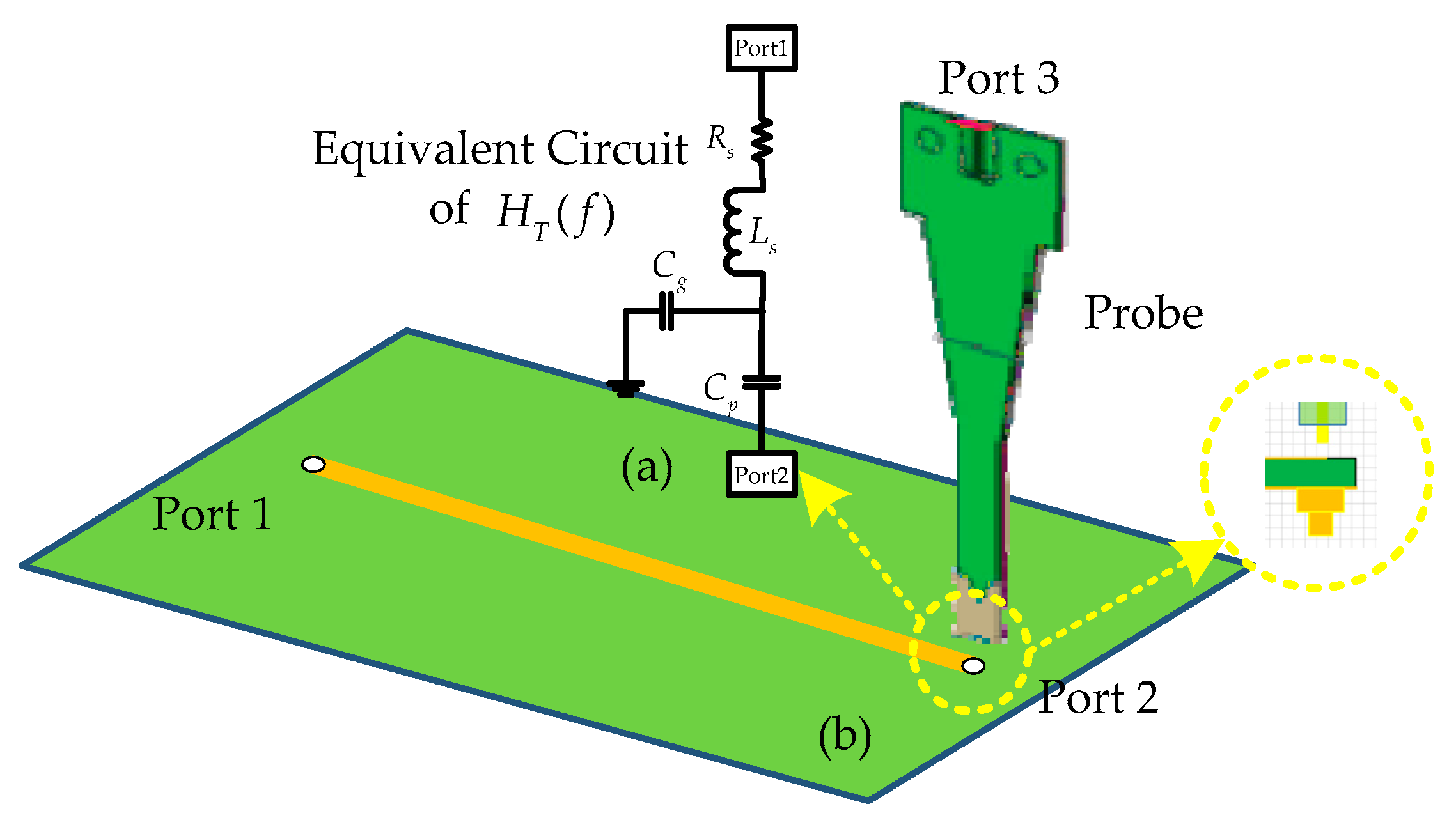
2. The Principle of Extracting Transmission Characteristics

For the near-field emission analysis, a wideband microstrip line electric probe is used [23]. As shown in Figure 1, a common near-field probe measurement system is illustrated. The printed trace, including straight lines, corners, and vias, is excited by a signal generator and matched by a load of 50 Ω. The probe is placed above the trace and connected to an SA to obtain the near-field emission spectrum. The microstrip line electric probes, similar to the coaxial probes, utilize capacitive coupled probing [24]. The coupling capacitance between the printed trace and the probe tip is C p . The voltage generates a time-varying electric field that induces a current signal i c in C p flowing to the detecting tip. The current can be calculated as
i c = C p A d E ( t ) d t ,
where E ( t ) is the electric field strength, t denotes time variable, and A is the system factor.
Based on the theory [25], the system consisting of the electric probe and the printed trace can be presumed to be a linear and time invariant (LTI) system. The principle of the extraction of transmission characteristics from a spectrum has two important components. Firstly, as shown in Figure 1, the input voltage v i n ( t ) of the LTI system on port 1 is a wideband signal, v l ( t ) is the voltage on the connector of the printed trace (port 2), and the output is the induced voltage v p ( t ) on the probe tip (port 3). Through convolution, the relationships between the voltages v i n ( t ) , v l ( t ) , and v p ( t ) can be written as
v l ( t ) = v i n ( t ) ( t τ ) h l ( τ ) d τ ,
and
v p ( t ) = v l ( t ) ( t τ ) h t ( τ ) d τ ,
where h l ( τ ) is the response of the printed trace and h t ( τ ) is the response of the induction process. By converting them to the frequency domain, we have
V L ( f ) = V I N ( f ) H L ( f ) ,
and
V P ( f ) = V L ( f ) H T ( f ) ,
where V I N ( f ) , V L ( f ) , and V P ( f ) denote the Fourier transforms of v i n ( t ) , v l ( t ) , and v p ( t ) , respectively. H L ( f ) is the transmission coefficient of the printed trace, and H T ( f ) is the transfer function of the induction process shown in Figure 1. When one is considering the whole system, according to Equations (3) and (4), H L ( f ) can be derived as
H L ( f ) = V P ( f ) V I N ( f ) H T ( f ) .
In Equation (5), V P ( f ) can be measured by an SA; H T ( f ) can be measured by a VNA or a simulation or a model. Once V I N ( f ) is determined, the transmission characteristics of the interconnects can be calculated from Equation (6). Therefore, next, we discuss how to reconstruct the input signal V I N ( f ) from the output V P ( f ) and how to extract the transmission characteristics from the near-field emission.
Secondly, for printed traces, considering the quality of signal transmission, they are commonly low-pass linear systems. The transmission characteristic function H L ( f ) of the interconnects can be written as
H L ( f ) = { H P ( f ) , f < f c H C ( f ) , f f c ,
where H P ( f ) is the transmission coefficient in the pass band, H C ( f ) is the transmission coefficient in the stop band, and f c is the cut-off frequency. In the pass band, there is virtually no attenuation. Hence, after normalization, we have
| H P ( f ) | 1   or   | H P ( f ) | d B 0 ,
where | H P ( f ) | d B is the decibel form of the transmission coefficient in the pass band. According to Equation (3), V L ( f ) can be derived as
V L ( f ) = V I N ( f ) H L ( f ) V I N ( f ) , f < f c .
Therefore, when V L ( f ) is calculated using Equation (4), V I N ( f ) below f c is also derived. Based on that, the time domain waveform v i n ( t ) can be reconstructed using the parameters extracted from the partial spectrum of V I N ( f ) [26]. Afterwards, V I N ( f ) in the whole frequency domain can be calculated according to
V I N ( f ) = F { v i n ( t ) } ,
where F represents the Fourier transforms.
According to the above derivation, the process of preforming the transmission characteristic extraction from the near-field emission of interconnects in a PCB is as follows. Firstly, a microstrip line electric probe connected to an SA is placed right above the tested trace to measure the output near-field emission spectrum V P ( f ) of the wideband signal flowing in the printed trace. Secondly, the electromagnetic field simulation, VNA testing, or equivalent circuit modeling is conducted to obtain the transfer function H T ( f ) . Thirdly, the time domain parameter extraction method is used to obtain the whole band input signal spectrum V I N ( f ) . Finally, data for V P ( f ) , H T ( f ) , and V I N ( f ) are utilized to calculate the transmission function H L ( f ) according to Equation (6). Note that the methods of the transfer function H T ( f ) modeling and the whole band spectrum of input signal V I N ( f ) estimation are shown in the following sections.

3. The Key Technologies of Extracting Transmission Characteristics

3.1. Obtaining The Transfer Function H T ( f )

H T ( f ) is related to the structures of circuits and is disparate for different transmission lines and connectors. In this study, a coplanar waveguide with a through-hole SMA connector soldered at the end was employed. The equivalent circuit of H T ( f ) is shown in Figure 2a. The coupling capacitance C p between the printed trace and the probe tip play an important role in coupling, which is only related to the geometric structure. A plane-parallel capacitor is appropriate for this structure. The value can be estimated according to
C p = ε S h ,
where ε denotes the permittivity of the medium, S denotes the area of the plates, and h denotes the distance between the plates. The equivalent circuit composed of RLC elements was deduced [15] for the microstrip line electric probe. The loss resistance R s (=3.6 Ω), the self-inductance L s (=16 nH), and the shunt capacitance C g (=8.5 pF) of the probe effect the transfer factor drastically at a high frequency.
To characterize and validate H T ( f ) , a coupling measurement and a commercial finite element field simulation were arranged. Figure 2b illustrates the model of the probe and PCBs with connectors in a simulator. As shown in Figure 3, a VNA and a probe fixture are used to maintain the position between the probe and the printed trace being tested. There are three ports. Port 1 is one end of the printed trace, and port 2 is the other end connected to a 50 Ω terminal. Port 3 is the probe output, and port 1 and port 3 are connected to the VNA. The measurement results with standardized calibration and simulation of H T ( f ) are shown in Figure 4 with different distances (0.5 mm and 1.5 mm) between the fixed probe and tested printed trace, and they are compared with those of the equivalent circuit model.
The distance between the probe and printed trace is the major factor affecting C p in this system because the area is constant when the probe is right above the printed trace. The values are 118 fF and 37 fF, respectively, when the distances are 0.5 mm and 1.5 mm, according to Equation (10). Figure 4 shows that the equivalent circuit model and field simulation agree well with the measurement curves at a low frequency (<4 GHz). The reason for this is that the fringe effect cannot be ignored at a high frequency. Therefore, at a high frequency, the measurement data are chosen to characterize H T ( f ) .

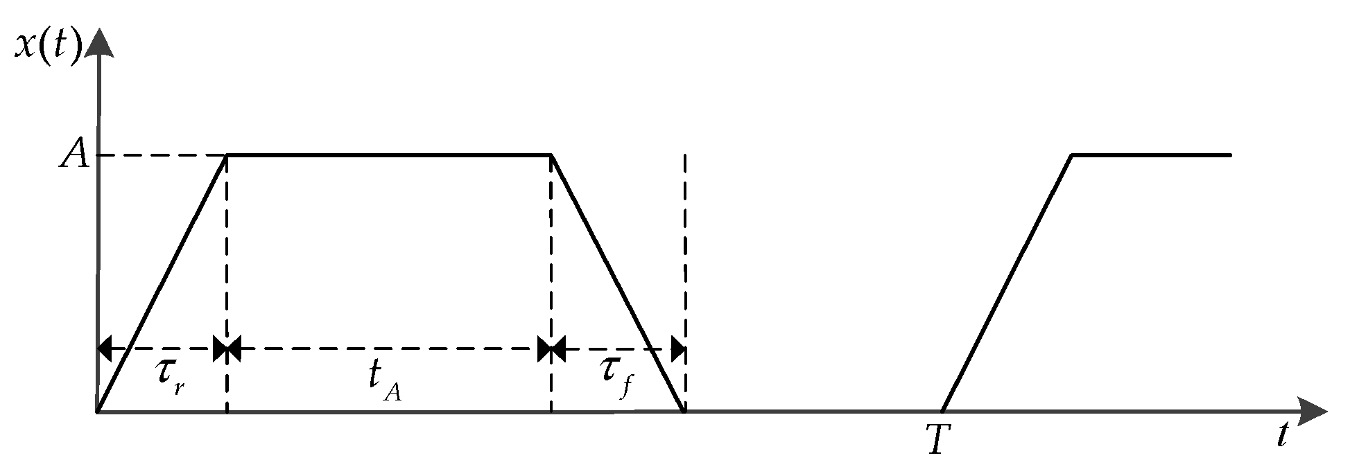
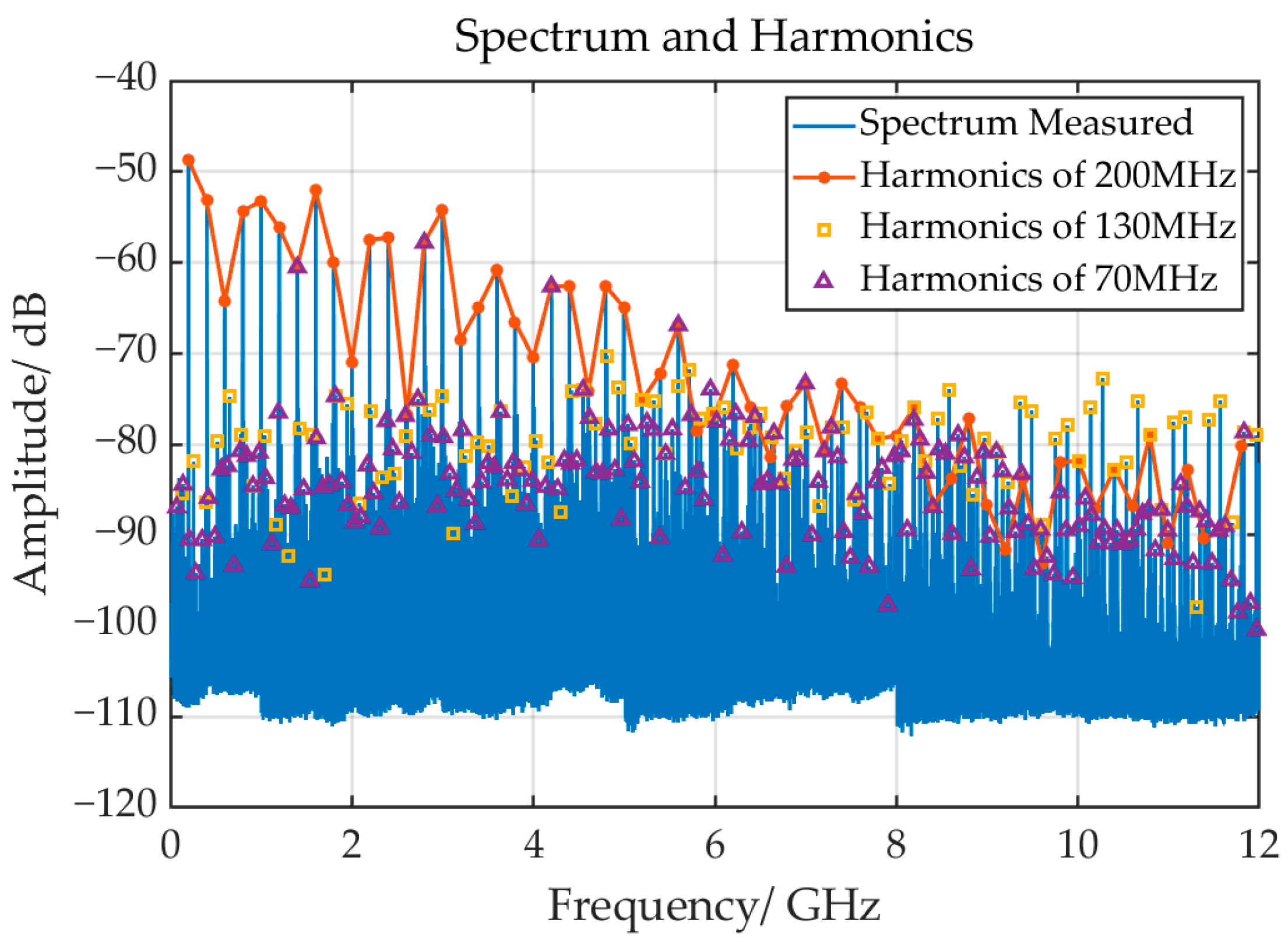
3.2. The Input Signal Estimation

Trapezoidal signals were chosen as the wideband input of the printed trace because they can generate a significant number of electromagnetic emissions in most digital circuits and switched-mode power supplies. A trapezoidal signal in the time-domain is illustrated in Figure 5. These parameters, including amplitude A , period T , rise time τ r , high-voltage time t A , and fall time τ f , are used to express the trapezoidal signal in the time domain. Based on the positive frequency Fourier series [27], the trapezoidal signal can be written as
v ( t ) = c 0 + n = 1 + | c n | cos ( 2 n π f 0 t + c n ) , n N ,
c n = j A π n e j n π ( 1.5 D 1 + D 2 + 0.5 D 3 )
[ S a ( n π D 1 ) e j n π ( 0.5 D 1 + D 2 + 0.5 D 3 ) S a ( n π D 3 ) e j n π ( 0.5 D 1 + D 2 + 0.5 D 3 ) ] ,
where f 0 = 1 / T denotes the fundamental frequency of the signal, n f 0 denotes harmonics of that fundamental frequency, c n represents the expansion coefficients (they may have a complex value, denoted by c n = | c n | c n ), and D 1 , D 2 , and D 3 denote the proportions of the rise time, high-voltage time, and fall time, respectively.
When the amplitudes of the emission spectrum are obtained for f < f c , according to Equation (8), the spectrum of the input signal for f < f c is also obtained. Then, we extract the time parameters from the partial spectrum of the input signal. Since the expansion coefficients are in terms of cyclic frequency f 0 , when the fundamental frequency f 0 is extracted, the amplitude of the spectral components | c n | can be obtained. Then, according to Equation (12), the parameters D 1 , D 2 , and D 3 are extracted. To guarantee the high accuracy of the reconstruction, f c must be at least greater than 3 f 0 .
The fundamental frequency f 0 can be calculated using the method in [8], which is based on the autocorrelation function. For periodic signal f ( t ) = f ( t + T ) , the autocorrelation function R ( τ ) can be written as
R ( τ ) = + f ( t ) f ( t τ ) d t = + f ( t ) f ( t ( τ + T ) ) d t = R ( τ + T ) .
Therefore, the autocorrelation function of the periodic signal is also periodic with the same repetition period. For the superposition of several periodic signals, when τ = n T , n N , R ( τ ) will reach maximal values, the period T can thus be extracted by calculating the autocorrelation function. Then, the parameters D 1 , D 2 , and D 3 can be obtained by fitting the practical measured harmonic amplitudes | A n | into the AWDO algorithm [27]. When the initial values of the parameters D 1 , D 2 , and D 3 are obtained, the first calculated harmonic amplitudes | c i | according to Equation (12) are compared with the practical measured | A i | . If the root-mean-square error (RMSE) disagrees with the setting condition, the parameters must be changed and compared repeatedly. The iteration will be finished until it agrees with the RMSE setting, such as
Minimize   e r r o r R M S E = 1 N i = 1 n [ 20 log 10 ( | c i ¯ | | A i ¯ | ) ] 2 ,
where A i ¯ denotes the normalization amplitudes of the ith practical measured harmonic amplitude with decibel form and c i ¯ is the normalization amplitude of the ith predicted harmonic amplitude. Finally, the parameters D 1 , D 2 , and D 3 are exported. Table 1 shows the results. The error is no more than 3%, indicating that the method can extract the time domain parameters from spectrum amplitudes accurately. When D 1 , D 2 , and D 3 are extracted, the amplitudes of harmonic amplitudes in the whole measured band can be obtained according to Equation (12).

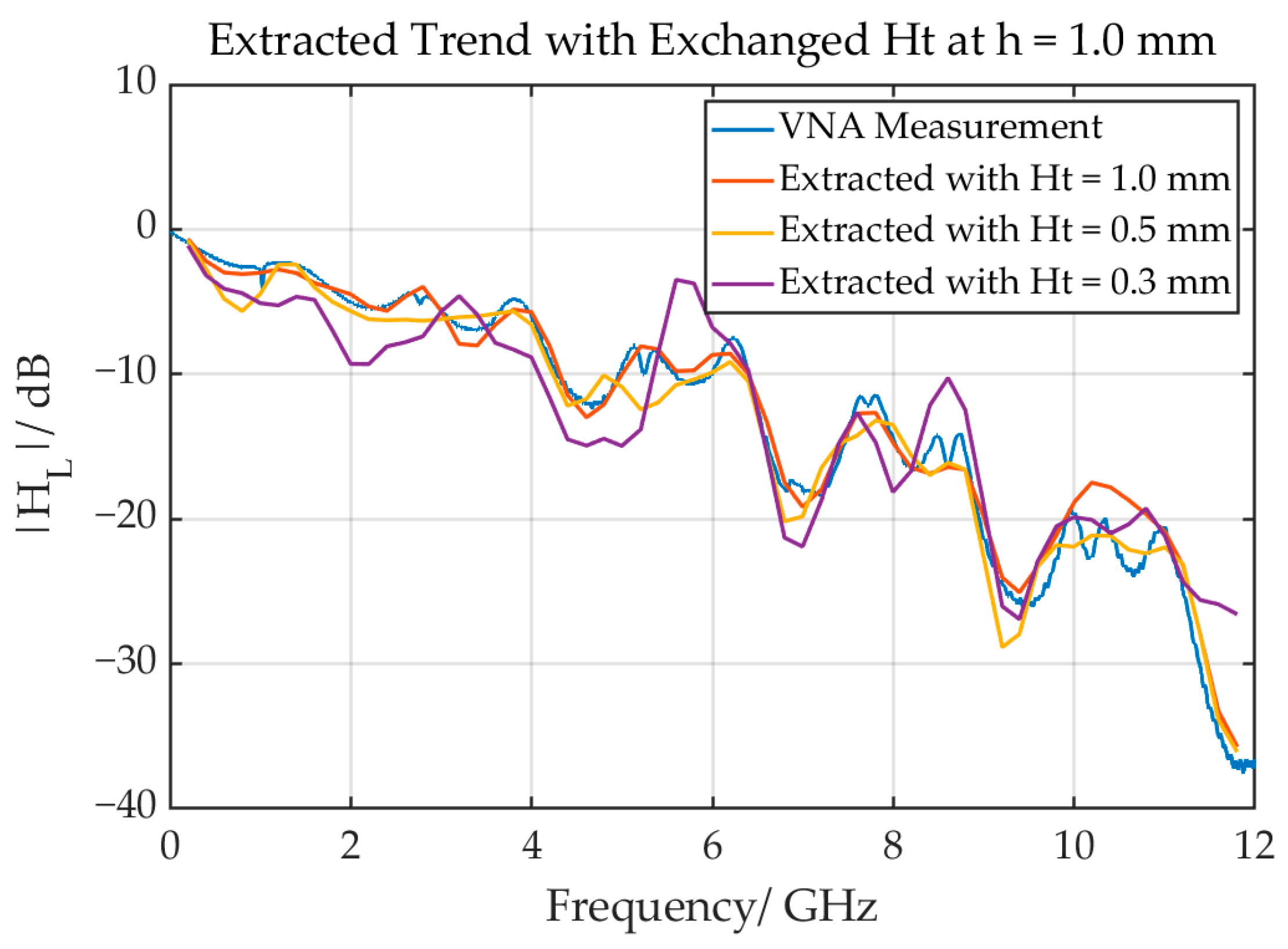
4. Validation and Error Analysis of Extracting Transmission Characteristics

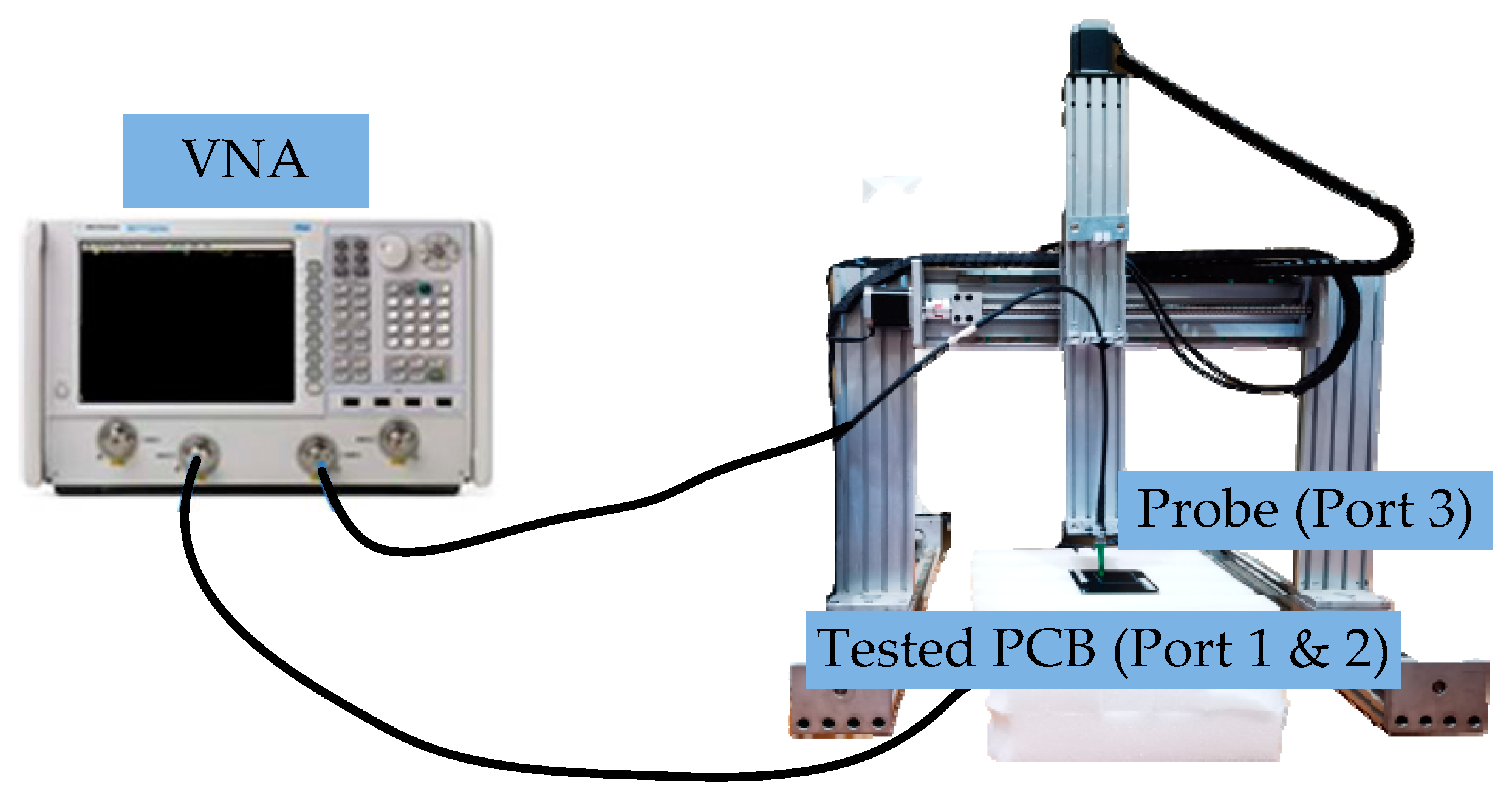
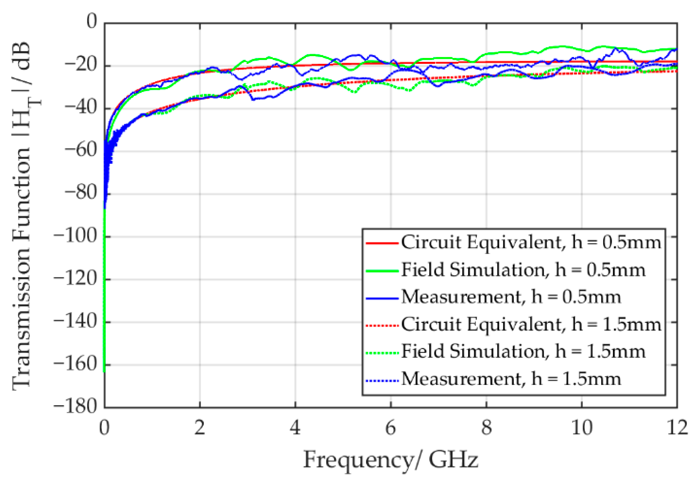
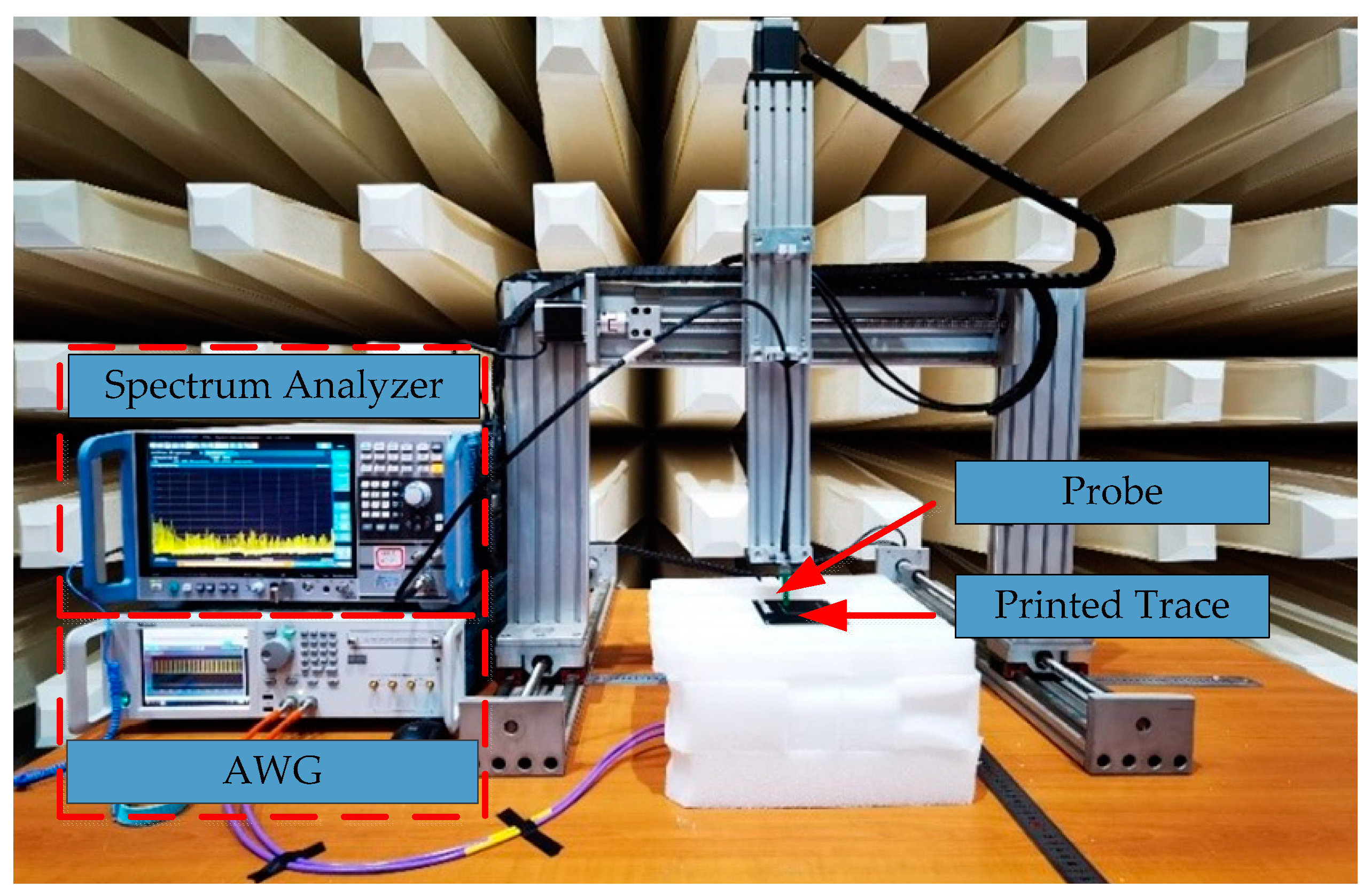
4.1. Experiment Validation

The setup of the validation experiment for the extraction of transmission characteristics from the near-field emission is shown in Figure 6. The probe was secured to the bracket, which is right above the printed trace and perpendicular to the ground. Arbitrary waveform generators (AWG) were connected to the ends of the printed traces for the signal injection, and the other ends of the traces were connected to 50 Ω terminals to guarantee steady signal transmission, while the output of the probe was connected to an SA.
The proposed method was validated using two types of circuits: one has only one trace with different discontinuities, which was first measured to verify the accuracy of the method, and the other one has many traces fabricated on PCBs, and it was used to validate the effectiveness of complicated structures with the interference signal.

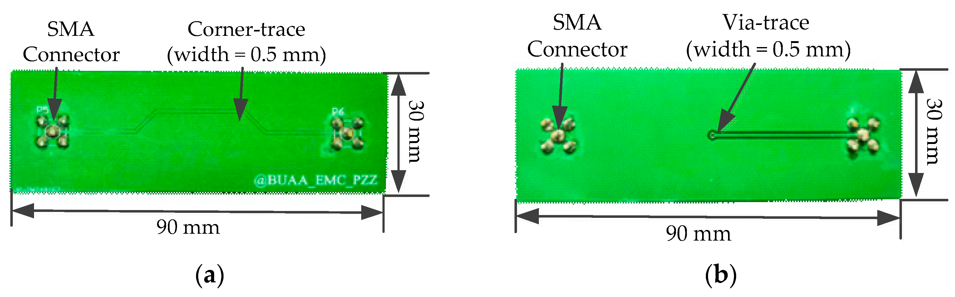
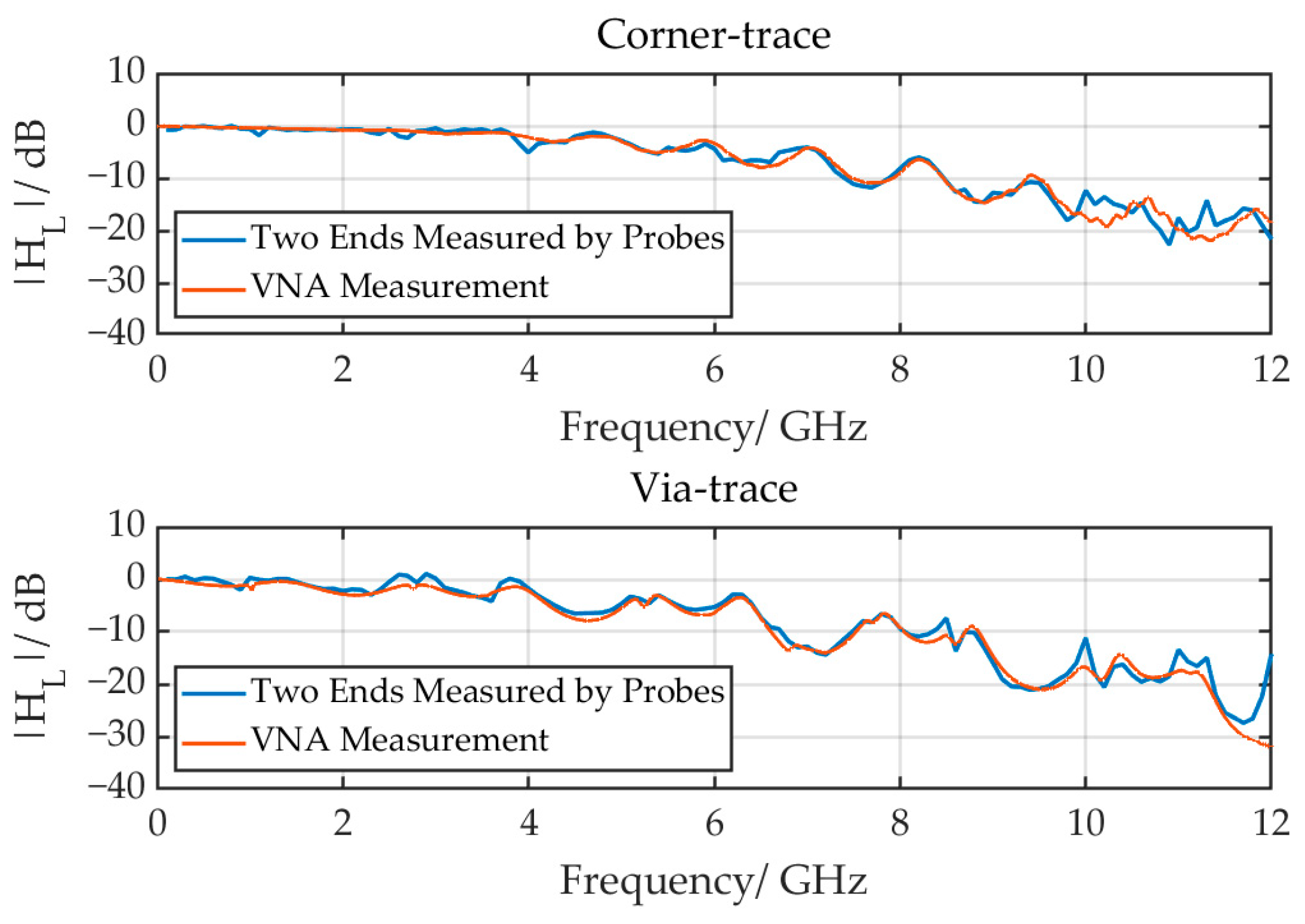
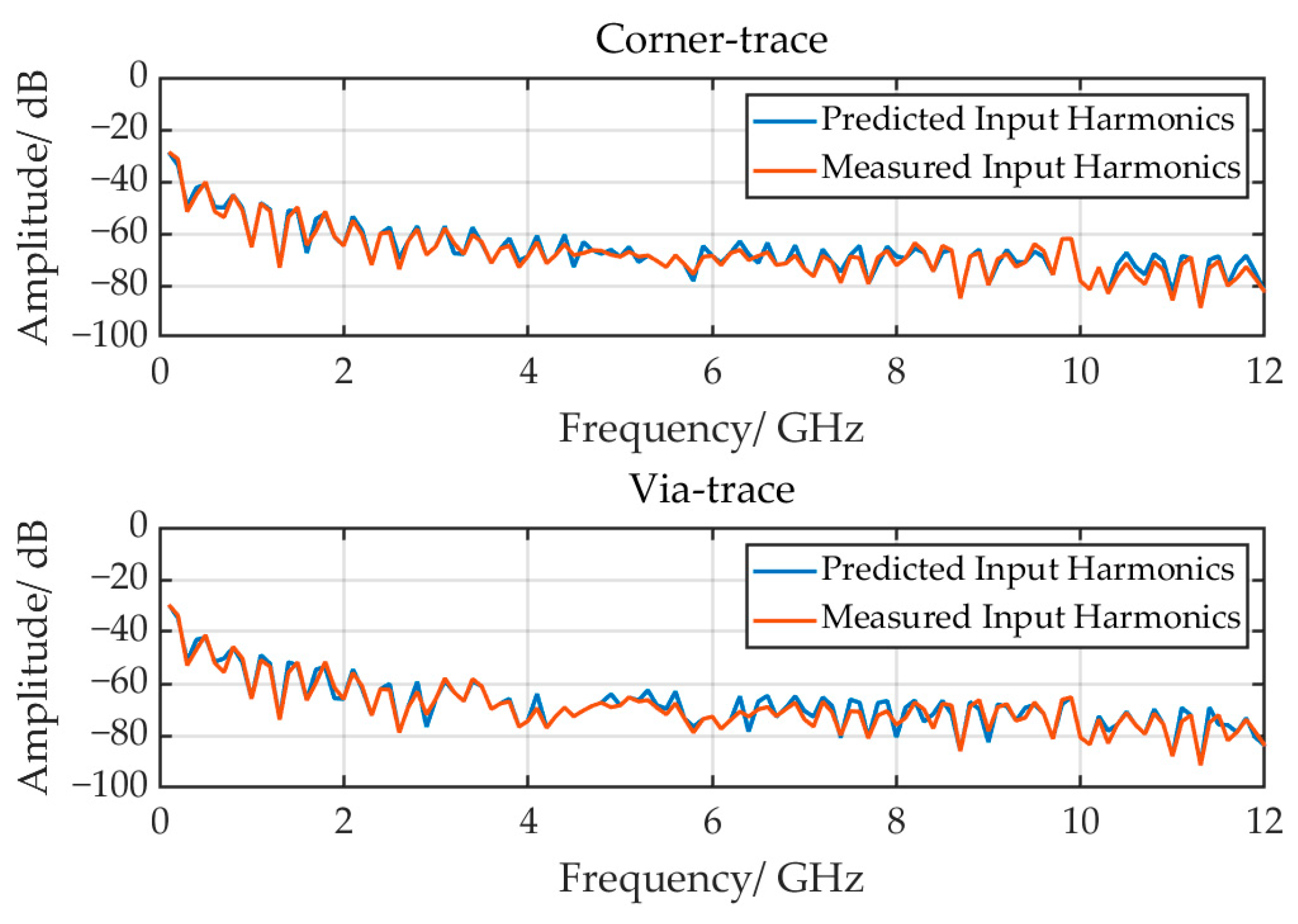
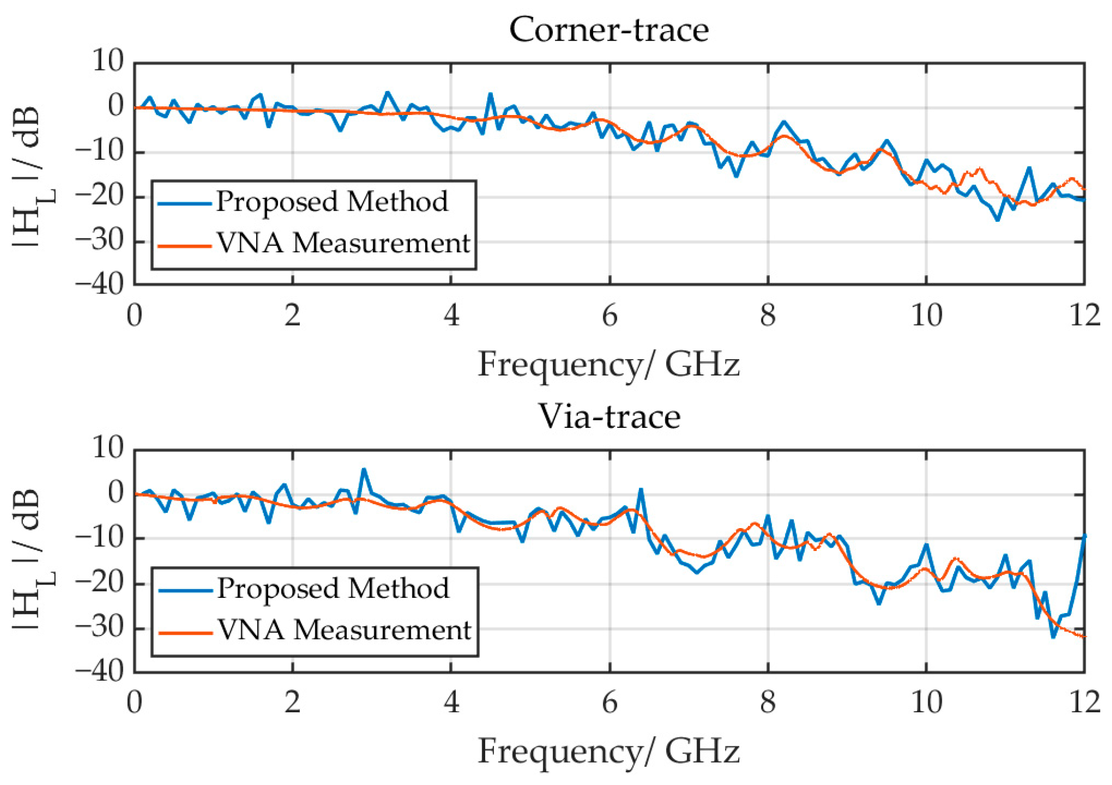
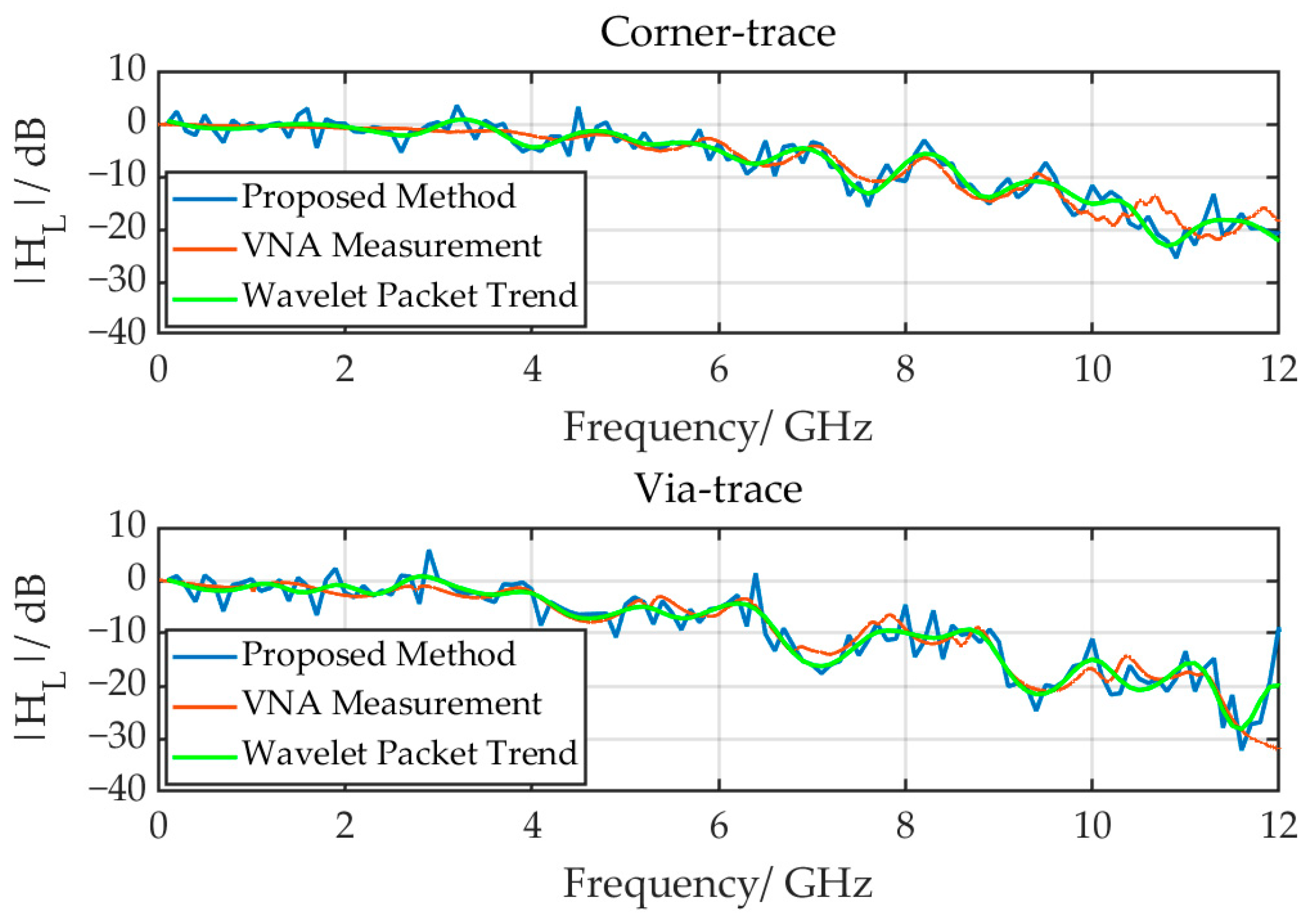
4.1.1. One-Trace Validation

One-trace validation was performed with two kinds of printed traces, a corner trace and a via trace, as shown in Figure 7. Both PCBs had two layers and were produced from 1.6 mm thick FR4 substrate ( ε r = 4.3 ) with dimensions of 90 mm × 30 mm. The corner trace had a 0.5 mm wide trace and four 135 degree corners printed on the top layer, constructing a coplanar waveguide with the ground planes, and two through-hole SMA connectors were soldered at both ends of the printed trace. The width of the via trace was 0.5 mm, which was crossed at the center of the board by a 1.27 mm via, producing a coplanar waveguide with the ground planes. There are also two through-hole SMA connectors soldered at both ends of the printed trace, so that the signal can be injected into the trace.
To verify the transfer function H T ( f ) , a 100 MHz trapezoidal waveform was injected to the tested printed trace, and the emission spectrum was measured at both ends of the trace. The distance between the tip of probe and the tested printed trace was 0.5 mm. The transmission coefficient was calculated by subtracting the amplitude of the emission spectrum tested at the load side from that which was tested at the input side in decibels. It was compared with the results obtained directly using a VNA. The amplitude of the original spectrum, the extracted harmonic amplitudes, and the corrected harmonic amplitudes of input signal and load signals are shown in Figure 8. Figure 9 shows that the transmission characteristics H L ( f ) of a corner trace and a via trace obtained by two-sided measurement and VNA measurement are in good agreement up to 12 GHz. The mean variations of the two printed traces are 1.32 dB and 1.57 dB, respectively. The maximum errors are 5.6 dB at 11.3 GHz and 16.3 dB at 12 GHz, respectively, which shows that H T ( f ) is effective.
When only the load side was measured, a trapezoidal waveform of 100 MHz was injected to the tested printed trace. Figure 10 depicts the amplitudes of the predicted and measured input harmonics of the above two traces. The transmission characteristics H L ( f ) acquired with the proposed method are compared with those measured using VNA in Figure 11. A wavelet packet [28] was applied to smooth the curves, as shown in Figure 12. After being processed, the transmission coefficients calculated with the proposed method agreed well with those obtained using a VNA below 12 GHz. The mean variation of the corner trace is 3.18 dB, and the maximum error is 6.7 dB at 11.3 GHz. The mean variation of the via trace is 3.52 dB, and maximum variation is 17.2 dB at 12 GHz. Except for 12 GHz, they can satisfy the requirements for engineering utilization.

4.1.2. Multi-Traces Validation
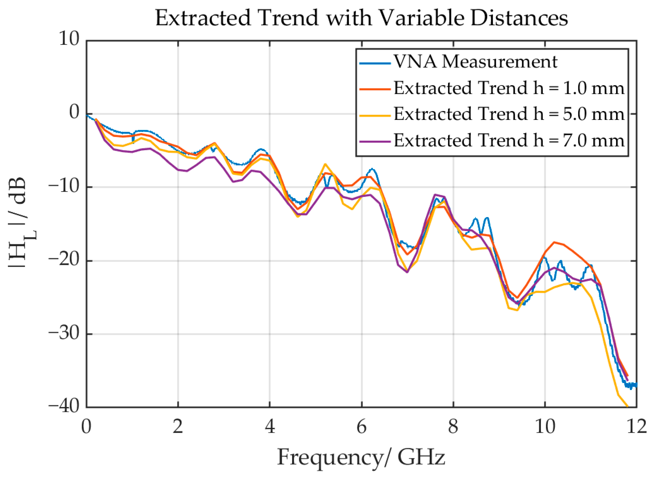
A multi-trace structure is shown in Figure 13. There are six traces printed on a 1.6 mm thick FR4 ( ε r = 4.3 ) substrate board. On the bottom of the substrate board, a ground was placed, forming microstrips with the upper traces. The board is 100 mm × 100 mm in size. Six through-hole SMA connectors with an equal interval of 8.8 mm were soldered at both edges of the board and connected by parallel corners traces, respectively. A coupling zone in the center of the board was formed by traces routed side-by-side with 0.5 mm of clearance, and the width of each trance was 0.76 mm. When the board was placed on the test platform shown in Figure 6, various signals were injected through the ports on one side, creating an interference environment.
To analyze the issue simply, we selected three traces for signal injection. Trapezoidal waveforms of 70 MHz, 200 MHz, and 130 MHz were injected into the printed traces through port 3, port 5, and port 7, respectively. The probe was positioned 0.5 mm vertically above port 6; the transmission characteristics from port 5 to port 6 were calculated. Firstly, the fundamental frequencies were obtained by using the method introduced in Section 3.2. Secondly, we scanned the three traces to determine which fundamental frequency had the highest amplitude when the probe was above port 6, and then we identified the signal transmitted on the trace. Finally, the transmission characteristic was calculated according to the identified signal by the proposed method. Figure 14 shows the spectrum measured above port 6, as well as the harmonics of signal transmitted from port 5 to port 6. The transmission characteristic of the trace from port 5 to port 6 obtained by the proposed method and smoothed by wavelet packet were compared with measured by a VNA in Figure 15. The analysis results indicate that the calculation results of this paper are in good agreement with the VNA data. The mean variation and maximum error are 2.78 dB and 4.22 dB at 10.4 GHz, respectively.

4.2. Error Analysis

From the above analysis, we can see that the two key points, the transfer function H T ( f ) and the input signal V I N ( f ) , affect the accuracy of H L ( f ) . In practice, H T ( f ) is correlated to the coupling capacitance, which is dependent on the distance between the printed trace being tested and the near-field probe tip, but the amplitude of V I N ( f ) is normalized, which partially cancels out the error caused by the height. To investigate the influence of the distance on transmission characteristic extraction, the variable height and height resolution were considered. The via trace was chosen as the validated structure; the compared results of the transmission characteristic extraction at 1 mm, 5 mm, and 7 mm distances and those obtained using the VNA are depicted in Figure 16. We can see that at different distances between the printed trace and the probe, the extracted results agree well. On the other hand, we considered the height resolution of the tested distance at 1 mm, but the transfer function exchanged with H T ( f ) at 0.3 mm and 0.5 mm. Figure 17 displays the compared results. It shows that when height deviation is about 0.5 mm, it seems to be easier to control and the obtained transmission characteristic is still in good agreement with the standard vector network analyzer (VNA) measurements. Furthermore, considering the random perturbations in the testing process, there are ±3 dB random fluctuations added to every harmonic amplitude at a 1.0 mm distance in order to verify the method against conventional random interference, respectively. Figure 18 depicts the result of the random perturbations condition, which is compared to no perturbations and VNA measurement.
Furthermore, it is hardly guaranteed that the positions in each test are consistent. We have employed the technique of averaging several measurements to minimize the error. Furthermore, the harmonic spectra of V I N ( f ) reconstructed using mathematical formulae cannot be exactly the same as the practical harmonics due to the signal processing flow, including analog-to-digital conversion, the filter, and so on. It could introduce errors and affect the calculation of the transmission characteristics. We have amended the deviation using preliminary test data. Generally, for a transmission characteristic error less than 25% in the experiment, the maximum vertical distance error is controllable at 0.5 mm. It should be noted that the allowed maximum vertical distances depend on the size of the tip and width of the printed trace being tested.

5. Conclusions

In this paper, a method for extracting transmission characteristics of interconnects in printed circuit boards (PCBs) from near-field emission was proposed. A wideband microstrip line electric probe was adopted. The transmission characteristics were calculated by extracting the harmonic components from the measured emission. The harmonic components were firstly calculated by the transfer function between the probe and the tested printed trace, which was modeled by an equivalent circuit. Then, the harmonics were used to extract time domain parameters by an autocorrelation function and an optimization algorithm. Based on the time domain parameters, the input harmonic could be reconstructed. Therefore, the transmission characteristics were obtained. To validate the method, two kinds of one-trace structures, including a corner trace and a via trace, and a multi-trace structure were used. The transmission characteristics extracted by the proposed method were good agreement with the standard vector network analyzer (VNA) measurements up to 12 GHz. The error caused by the distance and the disturbance signal is analyzed.

Author Contributions

Conceptualization, Z.P., H.X. and D.S.; methodology, Z.P. and H.X.; software, Z.P. and H.X.; validation, Z.P.; investigation, Z.P.; resources, Z.P., H.X. and D.S.; data curation, Z.P. and H.X.; writing—original draft preparation, Z.P.; writing—review and editing, D.S., H.X. and Z.P.; visualization, Z.P.; supervision, D.S.; funding acquisition, D.S. All authors have read and agreed to the published version of the manuscript.

Funding

This research was funded by the National Natural Science Foundation of China under grant numbers 62293492 and 62293495.

Institutional Review Board Statement

Not applicable.

Informed Consent Statement

Not applicable.

Data Availability Statement

Not applicable.

Conflicts of Interest

The authors declare no conflict of interest.

References

  1. Yi, Z.; Chen, Z.; Tian, X. Design and characterisation of a dual probe with double-loop structure for simultaneous near-field measurement. IET Microw. Antennas Propag. 2022, 16, 1751–8725. [Google Scholar] [CrossRef]
  2. Su, D.; Xie, S.; Chen, A.; Shang, X. Basic Emission Waveform Theory: A Novel Interpretation and Source Identification Method for Electromagnetic Emission of Complex Systems. IEEE Trans. Electromagn. Compat. 2018, 60, 1330–1339. [Google Scholar] [CrossRef]
  3. Shang, X.; Su, D. Use Modified Lomb-Scargle Method to Analyze Electromagnetic Emission Spectrum. In Proceedings of the 2015 IEEE 6th International Symposium on Microwave, Antenna, Propagation, and EMC Technologies (MAPE), Shanghai, China, 28–30 October 2015. [Google Scholar]
  4. Su, D.; Zhu, K.; Niu, M.; Wang, X. A Quantified Method for Characterizing Harmonic Components from EMI Spectrum. In Proceedings of the 2015 Asia-Pacific Symposium on Electromagnetic Compatibility (APEMC), Taipei, China, 25–29 May 2015. [Google Scholar]
  5. Shang, X.; Su, D.; Zhu, K.; Xu, H. A Method for Time-Domain Parameters Identification from EMI Spectrum. In Proceedings of the 2016 Asia-Pacific International Symposium on Electromagnetic Compatibility (APEMC), Shenzhen, China, 18–21 May 2016. [Google Scholar]
  6. Su, D.; Zhu, K.; Xu, H.; Peng, Z.; Yang, S.; Liu, Y. An Accurate and Efficient Approach for High-Frequency Transformer Parameter Extraction. Chin. J. Electron. 2019, 28, 1059–1065. [Google Scholar] [CrossRef]
  7. Shang, X.; Su, D.; Xu, H.; Peng, Z. A Noise Source Impedance Extraction Method for Operating SMPS using Modified LISN and Simplified Calibration Procedure. IEEE Trans. Power Electron. 2017, 32, 4132–4139. [Google Scholar] [CrossRef]
  8. Hao, X.; Xie, S. A Multi-Source Model Extraction Method of Digital Circuit Conducted Emission. J. B. Univ. Aeronaut. Astronaut. 2021, 11, 2287–2296. (In Chinese) [Google Scholar]
  9. Boyer, A.; Nolhier, N.; Caignet, F.; Dhia, S. Closed-Form Expressions of Electric and Magnetic Near-Fields for the Calibration of Near-Field Probes. IEEE Trans. Instrum. Meas. 2021, 70, 2007315. [Google Scholar] [CrossRef]
  10. Gao, Y.; Wolff, I. Miniature Electric Near-Field Probes for Measuring 3-D Fields in Planar Microwave Circuits. IEEE Trans. Microw. Theory Tech. 1998, 7, 907–913. [Google Scholar]
  11. He, Z.; Wang, L.; Chen, L.; Luo, R.; Liu, Q. A Wideband Tangential Electric Field Probe and a New Calibration Kit for Near-Field Measurements. IEEE Trans. Microw. Theory Tech. 2022, 7, 3557–3565. [Google Scholar] [CrossRef]
  12. Stenarson, J.; Yhland, K.; Wingqvist, C. An In-Circuit Noncontacting Measurement Method For S-Parameters and Power in Planar Circuits. IEEE Trans. Microw. Theory Tech. 2001, 12, 2567–2572. [Google Scholar] [CrossRef]
  13. Zelder, T.; Geck, B.; Wollitzer, M.; Rolfes, I.; Eul, H. Contactless Vector Network Analysis with Printed Loop Couplers. IEEE Trans. Microw. Theory Tech. 2008, 11, 2628–2634. [Google Scholar] [CrossRef]
  14. Osofsky, S.; Schwarz, S. Design and Performance of a Noncontacting Probe for Measurements on High-Frequency Planar Circuits. IEEE Trans. Microw. Theory Tech. 1992, 8, 1701–1708. [Google Scholar] [CrossRef]
  15. Luo, C. Collocated and Simultaneous Measurements of RF Current and Voltage on a Trace in a Noncontact Manner. IEEE Trans. Microw. Theory Tech. 2019, 6, 2406–2415. [Google Scholar] [CrossRef]
  16. Hou, R.; Spirito, M.; Van Rijs, F.; Vreede, L. Contactless Measurement of Absolute Voltage Waveforms by a Passive Electric-Field Probe. IEEE Microw. Wirel. Compon. Lett. 2016, 12, 1008–1010. [Google Scholar] [CrossRef]
  17. Qiu, H. Movable Noncontact RF Current Measurement on PCB Trace. IEEE Trans. Instrum. Meas. 2017, 9, 2464–2473. [Google Scholar] [CrossRef]
  18. Müller, S.; Duan, X.; Kotzev, M.; Zhang, Y.; Fan, J.; Gu, X.; Kwark, Y.H.; Rimolo-Donadio, R.; Brüns, H.; Schuster, C. Accuracy of Physics-Based via Models for Simulation of Dense via Arrays. IEEE Trans. Electromagn. Compat. 2012, 54, 1125–1136. [Google Scholar] [CrossRef]
  19. Duan, X.; Rimolo-Donadio, R.; Müller, S.; Han, K.; Gu, X.; Kwark, Y.H.; Brüns, H.-D.; Schuster, C. Impact of Multiple Scattering on Passivity of Equivalent-Circuit Via Models. In Proceedings of the IEEE Electrical Design of Advanced Packaging and Systems, Hangzhou, China, 12–14 December 2011. [Google Scholar]
  20. Müller, S.; Duan, X.; Rimolo-Donadio, R.; Brüns, H.-D.; Schuster, C. Non-Uniform Currents on Vias and Their Effects in a Parallel-Plate Environment. In Proceedings of the IEEE Electrical Design of Advanced Packaging and Systems, Singapore, 7–9 December 2010. [Google Scholar]
  21. Dahl, D.; Duan, X.; Ndip, I.; Lang, K.; Schuster, C. Efficient Computation of Localized Fields for Through Silicon via Modeling up to 500 GHz. IEEE Trans. Compon. Packag. Manuf. Technol. 2015, 5, 1793–1801. [Google Scholar] [CrossRef]
  22. Khac Le, H.; Kim, S. Machine Learning Based Energy-Efficient Design Approach for Interconnects in Circuits and Systems. Appl. Sci. 2021, 11, 915. [Google Scholar] [CrossRef]
  23. Liu, W.; Yan, Z.; Min, Z. Design of Miniature Active Magnetic Probe for Near-Field Weak Signal Measurement in ICs. IEEE Microw. Wirel. Compon. Lett. 2020, 30, 312–315. [Google Scholar] [CrossRef]
  24. Zietz, C.; Armbrecht, G.; Schmid, T.; Wollitzer, M.; Geck, B. A General Calibration Procedure for Measuring RF Voltages and Currents Applied to the EMC Analysis of Automotive High-Voltage Power Networks. IEEE Trans. Electromagn. Compat. 2015, 5, 915–925. [Google Scholar] [CrossRef]
  25. Liu, W.; Yan, Z.; Wang, J. An Ultrawideband Electric Probe based on U-Shaped Structure for Near-Field Measurement from 9 kHz to 40 GHz. IEEE Antennas Wirel. Propag. Lett. 2019, 18, 1283–1287. [Google Scholar] [CrossRef]
  26. Fang, W. Noncontact RF Voltage Sensing of a Printed Trace via a Capacitive-Coupled Probe. IEEE Sens. J. 2018, 21, 8873–8882. [Google Scholar] [CrossRef]
  27. Su, D.; Xu, H.; Zhou, Z.; Liu, Y. An Improved Method of Trapezoidal Waves Time-Domain Parameters Extraction from EMI Spectrum. In Proceedings of the 2019 International Applied Computational Electromagnetics Society Symposium—China (ACES), Nanjing, China, 14–19 April 2019. [Google Scholar]
  28. Antonini, G.; Orlandi, A. Wavelet Packet-Based EMI Signal Processing and Source Identification. IEEE Trans. Electromagn. Compat. 2001, 43, 140–148. [Google Scholar] [CrossRef]
Figure 1. Analysis model of a microstrip line electric probe and printed trace system.
Applsci 13 02874 g001
Figure 2. Full-wave model of the probe and printed trace.
Applsci 13 02874 g002
Figure 3. Setup for the transfer function measurement.
Applsci 13 02874 g003
Figure 4. Comparison of | H T ( f ) | from circuit simulation, field simulation, and measurement.
Applsci 13 02874 g004
Figure 5. The periodic trapezoidal signal and its time domain parameters.
Applsci 13 02874 g005
Figure 6. The setup for the transmission characteristics extraction measurement.
Applsci 13 02874 g006
Figure 7. The one-trace validated structures. (a) Corner trace; (b) via trace.
Applsci 13 02874 g007
Figure 8. Amplitude of original, extracted, and corrected harmonics of the input and load signals.
Applsci 13 02874 g008
Figure 9. The extracted transmission characteristics of a corner trace and a via trace measured at both ends compared with those obtained using a VNA.
Applsci 13 02874 g009
Figure 10. Amplitude of predicted and corrected harmonics of the input signal.
Applsci 13 02874 g010
Figure 11. The compared results between the transmission characteristics of a corner trace and a via trace with the proposed method and those obtained using a VNA.
Applsci 13 02874 g011
Figure 12. The extracted transmission characteristics of a corner trace and a via trace measured using proposed method and their trends compared with those obtained using a VNA.
Applsci 13 02874 g012
Figure 13. The multi-trace-validated structure.
Applsci 13 02874 g013
Figure 14. The spectrum measured above port 6 and the harmonics of signal transmitted from port 5 to port 6.
Applsci 13 02874 g014
Figure 15. The transmission characteristic of the trace from port 5 to port 6 obtained by the proposed method and smoothed by wavelet packet were compared with measured by a VNA.
Applsci 13 02874 g015
Figure 16. The transmission characteristic extraction at 1 mm, 5 mm, and 7 mm distances.
Applsci 13 02874 g016
Figure 17. The transmission characteristic extraction at 1 mm distance with exchanged H T ( f ) .
Applsci 13 02874 g017
Figure 18. The transmission characteristic extraction at 1 mm distance with random perturbations.
Applsci 13 02874 g018
Table 1. Extracted results from 1st to 13th order or 8th to 20th order harmonic amplitudes.
ItemsPreset Values
(%)
Extracted Results
for 1st–13th (%)
Extracted Results
for 8th–20th (%)
D 1 2.001.942.01
D 2 30.0030.0830.05
D 3 3.002.952.98
Error
(%)
D 1 3.00.5
D 2 0.270.17
D 3 1.70.67
Disclaimer/Publisher’s Note: The statements, opinions and data contained in all publications are solely those of the individual author(s) and contributor(s) and not of MDPI and/or the editor(s). MDPI and/or the editor(s) disclaim responsibility for any injury to people or property resulting from any ideas, methods, instructions or products referred to in the content.

