Abstract
Optical on-chip wireless interconnection is an emerging technology that aims to overcome the communication bottleneck in computing architectures and in which multiple processing units are exploited for data-intensive applications. In this work, we propose an integrated dielectric Vivaldi antenna, which exhibits the same gain performances for both TE and TM input polarizations. Point-to-point on-chip communication links between two Vivaldi antennas are analyzed. Moreover, the effect of wave polarization on the link performances is numerically studied in on-chip multilayer structures in connection with the multilayer characteristic parameters, i.e., cladding layer thickness and refractive index. The numerical results show that, with the same antenna gain, TM polarization is affected by lower propagation losses when suitable cladding layer thickness and refractive index are considered.
1. Introduction
The performance improvement of future computer architectures is also related to overcoming the communication bottleneck at the inter- and intra-chip level. In fact, the communication among different processing units can limit the overall performance of the system. The extensive research efforts toward more efficient communication are motivated by the constant growth of the computational requirements of data-intensive applications. Networks-on-chip (NoCs) are the most assessed forms of technology that allow efficient communication through electrical links and switches and among different cores and/or processing units [1,2]. However, latency, multi-hop communication, and scalability are seen as potential limits to a continuous increase in the performances of electrical NoCs. Therefore, alternative solutions are being investigated, ranging from the integration of an optical communication layer to the wireless interconnection at millimeter wave frequencies [3,4,5,6].
Optical Networks-on-chip (ONoCs), i.e., the optical “wired” technology, are based on the integration into computing architectures of an optical layer, housing signal routing and processing components such as switches and filters [7,8,9,10]. Optical communication is characterized by high bit rates and low latencies, and it is incredibly promising for overcoming the communication bottleneck. In general, the signal routing in the ONoCs is achieved by employing resonant or non-resonant components [11,12,13]. Resonant devices, such as micro-ring resonators (MRRs) or photonic band gap components, are intrinsically narrow band devices. The resonance condition occurs at given wavelengths, which depend on the geometrical and on the optical characteristics of the device (e.g., geometrical size, periodicity, refractive index, etc.) [14,15,16,17,18]. The use of many resonant devices in the same network requires a fine tuning of the resonances (e.g., by thermal tuning) to guarantee efficient communication between the different network nodes, especially when multiple resonant wavelengths are associated to multiple communication channels [12,19,20]. This can result in a considerable increase in the overall power budget and in the device complexity due to the tuning circuitry.
Differently from resonant components, non-resonant ones, such as Mach–Zehnder Interferometers (MZIs), can achieve a broadband behavior and can allow the simultaneous switching of multiple communication channels [13,21]. Therefore, Dense Wavelength Division Multiplexing (DWDM) communication can be implemented to reach high aggregate data rates.
As the network size scales up and the number of transmitters and receivers increases, many routing devices are required, resulting in higher losses and crosstalk, especially due to waveguide crossings.
A recently proposed technology, which is an alternative to ONoCs, is based on Wireless Networks-on-chip (WiNoCs). This technology offers the possibility of simplifying the network topological constraints and of reducing the inter-router hops while guaranteeing low-latency and broadcast communication [6,22,23,24]. Moreover, the on-chip integrability of wireless networks is allowed by the use of mm- or THz-wave signals, which require very small antennas. However, the integration of miniaturized antennas (e.g., graphene antennas [25]) is not yet fully mature technology, and many research challenges are still open.
On-chip wireless optical communication is an emerging technology that can contemporarily exploit, at the chip level, the advantages of optical and of wireless communications [26,27,28,29,30]. The combination of optical wired and wireless communications can help to reduce the network complexity and the number of switching elements necessary for linking all the transmitters and all the receivers. Moreover, the possibility of reducing the network topological constraints can lead to the exploration of new communication paradigms.
It is worth mentioning that, at the optical frequencies, the attenuation due to wireless propagation in free space (i.e., homogeneous medium) can be very high, and it can reach tens of dBs for 1 cm length of propagation, as it can be roughly estimated by the well-known Friis formula [31]. This attenuation limits the maximum distance between the transmitter and the receiver, but high-gain antennas can compensate for the loss associated with the wireless signal spread.
Different configurations of dielectric and plasmonic antennas have been proposed in the literature for on-chip wireless communications [29,30,32,33,34,35]. The plasmonic antennas have very small dimensions (a few microns), but they suffer non-negligible losses due to plasmonic mode propagation in the lossy metal. These losses limit the maximum achievable antenna gain. For example, Yagi–Uda plasmonic nanoantennas can achieve directivities of about 10 dB [32,33]. Integrated plasmonic Vivaldi antennas have also been proposed as single radiators or in array configurations [34,35], reaching gains up to about 14 dB with antenna size in the order of 2 µm.
All-dielectric antennas have low losses butthey are less compact. For example, in [29] a high-gain (approximately 21 dB) dielectric antenna was demonstrated. The configuration consisted of a tapered waveguide and a series of rectangular directors for a total antenna length of about 15 µm.
The antenna gain is not the only significant parameter for the evaluation of the on-chip wireless link performances. In fact, on-chip wireless propagation does not occur in a homogeneous medium, but in a multilayer one. The typical structures of photonic integrated chips are composed of different materials tiled up in different layers. Indeed, the complexity of the on-chip wireless propagation medium influences the overall communication link performance, causing multiple reflections and multipath interference (thus making the Friis formula too simplified and inaccurate). In particular, as demonstrated by the authors in [36,37,38], the propagation in the multilayer medium can be beneficial in terms of propagation losses with respect to the propagation in a homogeneous medium, thanks to constructive interference.
In this paper, we aim to numerically investigate the effect of wave polarization (either transverse electric TE or transverse magnetic TM) in on-chip wireless communication. For this purpose, we first introduce the design of a polarization-insensitive, dielectric Vivaldi antenna, which has the same radiation characteristics, expressed in terms of antenna gain, in both polarizations. Then, the performances of different point-to-point links between two dielectric Vivaldi antennas are analyzed in connection with the variation in the multilayer medium characteristics (i.e., layer thicknesses and material refractive indices). We assume that the polarization is selected in input to the waveguide of the transmitting antenna, i.e., the input waveguide is excited either with a TE or with a TM mode through suitable grating couplers or polarization selectors [39,40,41,42,43,44]. The polarized wave is then radiated into the surrounding space and received at the output antenna, always keeping the same polarization.
Silicon nitride Si3N4 technology has been chosen in this paper as a case of study, but the Vivaldi antenna design criteria and the multilayer propagation analysis can be virtually extended to any technology. Silicon nitride (SiN) is one of the platforms, together with silicon-on-insulator (SOI), that enable the on-chip integration of the optical networks thanks to the compatibility with Complementary Metal-Oxide Semiconductor (CMOS) technology. The proposed dielectric antenna can be regarded as a building block for optical wireless NoCs (OWiNoCs). Moreover, thanks to its compatibility with standard optical integrated technology, this antenna building block can be combined with standard waveguide components, thus widening the possibility of network design exploration.
Because the proposed Vivaldi antenna has the same gain in the two polarizations, the different performances that will be evidenced in the following can be attributed to the effect of the polarization of the radiated wave and to its interaction with the multilayer medium. As it will be shown, by selecting the TM mode in input to the transmitting antenna, the overall performance of the point-to-point link can be significantly improved. This opens new possibilities for the design of on-chip optical wireless interconnection networks.
In Section 2, the antenna characteristics are investigated by considering either the TE or the TM polarizations of the optical mode launched in input to the SiN strip waveguide. In Section 3, we analyze the performances of transmission links in an on-chip multilayer structure for both the TE and the TM polarizations. Conclusions are finally drawn in Section 4.
2. Design of the Dielectric Vivaldi Antenna
The proposed integrated antenna is schematized in Figure 1, where the relevant geometrical parameters are highlighted. As anticipated, the antenna is constructed with a SiN slot waveguide tapered according to a Vivaldi profile, and it is directly coupled to an input SiN strip waveguide. This geometry has been chosen to guarantee wideband performance of the antenna, thus maximizing the bandwidth of the on-chip network.
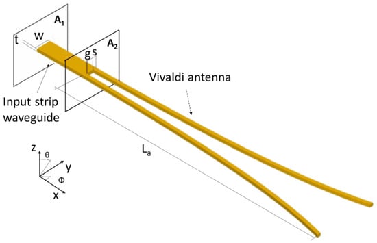
Figure 1.
Scheme of the dielectric Vivaldi antenna directly coupled to a strip waveguide. The antenna is composed of silicon nitride and, to investigate its radiation properties, it is embedded into a homogenous medium with refractive index nSiO2 = 1.445.
The Vivaldi profile can be calculated according to the following equations:
with
In Equation (2), R is the opening rate coefficient, whereas x1, y1 and x2, y2 are the edge coordinates of the Vivaldi profile in the xy plane.
The Vivaldi antenna is fed by a strip waveguide thanks to the direct coupling mechanism between the strip and the slot waveguides. The input optical signal of the strip waveguide is coupled directly to the slot mode, and then, it is radiated by the Vivaldi antenna. The radiation occurs predominantly toward the x direction in Figure 1, i.e., in front of the antenna.
The numerical model of the antenna was implemented through the three-dimensional Finite Difference Time Domain (3D-FDTD) method [45]. For the design of the antenna and the analysis of its radiation characteristics, the structure was assumed to be immersed in a homogenous medium with refractive index nSiO2 = 1.445 at the wavelength λ = 1.55 μm. This assumption eases the calculation of the far-field radiation diagrams because a homogeneous medium is required when the near-to-far-field transformations are performed.
In the proposed structure, the thickness of the waveguides was considered equal to t = 300 nm, as is the case in commercially available SiN samples. The dispersion of the refractive index of SiN [46,47] was included in the model, and the simulation domain was delimited by Perfectly-Matched-Layer (PML) boundary conditions.
The gain of the Vivaldi antenna depends on different geometrical parameters such as the width of the strip waveguide w, the slot gap g, and the length of the Vivaldi directors La. The initial total width of the slot waveguide, which opens according to the Vivaldi profile, is geometrically constrained by the width w of the input strip waveguide. Specifically, these geometrical parameters are linked according to the equation w = g + 2s, where w is the strip width, g is the initial gap of the slot Vivaldi antenna, and s is the width of the slot rails. The antenna gain can be optimized by changing the cross-section geometrical parameters (i.e., w, g, and s). For a given value of the strip width w, the gap g can be suitably chosen to maximize the gain. Moreover, once the antenna cross section has been optimized, the antenna gain can be further improved by changing the length La of the Vivaldi radiator.
In the following, we will consider three arbitrarily chosen values of the strip width w = 600 nm, w = 900 nm, and w = 1100 nm, which correspond to three different configurations identified by the letters A, B, and C, respectively. All the three considered values of the strip width w give the excitation of either a single TE or a single TM mode in the strip waveguide. By considering three different configurations, we aim to analyze the effect on the antenna gain induced by the cross-section geometrical parameters (i.e., w, s, and g) and to demonstrate that, given a certain strip width w, the gap g can be optimized to maximize the gain.
2.1. Direct-Mode Coupling Analysis
Although the modes that propagate in the strip and in the slot waveguides are, in principle, quite different (Gaussian- and non-Gaussian-like, respectively), the direct coupling of power between the two modes is possible, provided that their components overlap efficiently [48]. The overlap integral between the two modes can be calculated by the following rigorous formula [48]:
where E1 and E2 are the electric field components in the strip and in the slot waveguides, respectively, and and are the complex conjugates of the corresponding magnetic field components.
In order to analyze the direct coupling mechanism between the strip waveguide and the slot one, the electric and magnetic field components were calculated at the two sections denoted in Figure 1 as A1 and A2 by the Discrete Fourier Transform (DFT) of the time domain fields obtained via 3D-FDTD simulation of the whole structure. Sections A1 and A2 in Figure 1 correspond, respectively, to the strip and to the slot waveguides. The overlap integral of Equation (3) was calculated, either for the TE or for the TM fundamental modes, considering the electric and magnetic field distributions at these two sections.
Figure 2 shows the overlap integral that was calculated according to Equation (3) and as a function of the slot gap g for the TE (solid curves) and the TM (dashed curves) fundamental modes of the strip and of the slot waveguides. The results for the three chosen configurations are reported: width w = 600 nm (configuration A—blue curves), w = 900 nm (configuration B—red curves), and w = 1100 nm (configuration C—yellow curves). As it can be seen in Figure 2, the overlap integral is always above 0.9, thus allowing an efficient coupling of the optical signal from the strip to the Vivaldi antenna. Once the strip mode is coupled to the slot one, it propagates along the Vivaldi antenna being radiated in the surrounding medium.
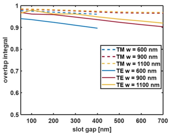
Figure 2.
Overlap integral calculated according to Equation (3) as a function of the initial slot gap value g. The blue, red, and yellow curves correspond to configurations A (w = 600 nm), B (w = 900 nm), and C (w = 1100 nm), respectively. For each value of the slot gap g, the slot rail width s can be calculated from the formula s = (w − g)/2. The wavelength is λ = 1.55 µm.
2.2. Vivaldi Antenna Radiation Analysis
In order to investigate the radiation characteristics of the proposed Vivaldi antenna, the far-field of the Vivaldi antenna coupled to the strip waveguide was evaluated by simulating the overall structure via the 3D-FDTD method. For this purpose, near-to-far field projections of the DFT-transformed electromagnetic fields were calculated on a closed surface surrounding the antenna and the strip waveguide [45]. In the evaluation of the radiation characteristics, the antenna was considered to be embedded in a homogeneous medium (with refractive index nSiO2 = 1.445) as required by near-to-far field projection calculation. The antenna gain G(θ,ϕ) is defined as:
where I(θ, ϕ) is the radiation intensity in spherical coordinates, and Pin is the input power launched into the strip waveguide [49].
As an example of the radiation characteristics of the Vivaldi antenna, Figure 3a,b show the gain as a function of (a) the angle θ (with Φ = 0) and (b) the angle Φ (with θ = π/2), for the TE (solid curves) and TM (dashed curves) modes, in the case of the Vivaldi antenna with strip width w = 900 nm, slot gap g = 300 nm, slot rail width s = 300 nm, and antenna length La = 25 μm. Moreover, Figure 3c,d report the electric field pattern of the Vivaldi antenna, which is calculated via 3D-FDTD in the xy plane for z = 0 μm (i.e., in the middle of the antennas) for the TE and TM polarizations. The geometry of the Vivaldi antenna is also evidenced by the black lines in Figure 3c,d. The color bar represents the normalized amplitude of the electric field in logarithmic scale. It is worth pointing out that the field patterns of Figure 3c,d are calculated in the antenna region at the wavelength λ = 1.55 µm via DFT of the time domain fields. Therefore, they are not far-fields, but they can help to qualitatively explain the far-field radiation diagrams.
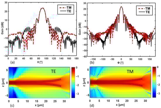
Figure 3.
(a,b) Gain as a function of (a) the angle θ (with Φ = 0) and (b) the angle Φ (with θ = π/2), for the TE (solid curves) and TM (dashed curves) modes in the case of the Vivaldi antenna with strip width w = 900 nm, slot gap g = 300 nm, slot rail width s = 300 nm, and antenna length La = 25 μm. (c,d) Electric field pattern calculated via 3D-FDTD in the xy plane for z = 0 μm (i.e., in the middle of the antennas) for the TE (c) and TM (d) polarizations. The color bar represents the normalized amplitude of the electric field in logarithmic scale. The wavelength is λ = 1.55 µm.
For the sake of comparison, we also consider the radiation characteristics of a simple truncated waveguide with width w = 900 nm (Figure 4a,b). The truncated waveguide can also be considered as an antenna because it radiates the propagating mode in the surrounding medium due to the abrupt termination. The gain curves in the vertical (a) and in the horizontal (b) planes are reported in Figure 4a,b for the truncated strip waveguide of width w = 900 nm for the TE (solid curve) and TM (dashed curve) modes. Moreover, the field patterns calculated for the truncated waveguide in the xy plane are also reported in Figure 4c,d.
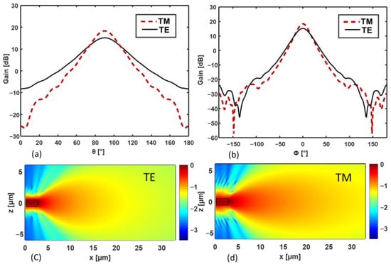
Figure 4.
(a,b) Gain as a function of (a) the angle θ (with Φ = 0) and (b) the angle Φ (with θ = π/2), for the TE (solid curves) and TM (dashed curves) modes in the case of the truncated waveguide. (c,d) Electric field pattern calculated via 3D-FDTD in the xy plane for z = 0 μm (i.e., in the middle of the antennas) for the TE (c) and TM (d) polarizations. The color bar represents the normalized amplitude of the electric field in logarithmic scale. The wavelength is λ = 1.55 µm.
As can be seen in Figure 3a,b, in the case of the analyzed Vivaldi antenna, the gain curves for the TE and the TM polarizations are very similar, especially in the main radiation lobe. This does not happen for the truncated waveguide (Figure 4a,b). Moreover, as the field patterns in Figure 3c,d show, the Vivaldi-shaped directors contribute to narrowing the radiated beam and to increasing the maximum gain with respect to the simple truncated waveguide structure (Figure 4c,d). Spurious radiation also occurs along the directors, causing sidelobes in the Vivaldi antenna radiation diagram.
Considering the reference axes in Figure 1, the maximum values of the Vivaldi antenna gain occur for Φ = 0 and θ = π/2, and they are equal to 23.8 dB and 23.52 dB for the TE and the TM modes, respectively. Therefore, the analyzed Vivaldi antenna can be considered polarization-insensitive, in the sense that it has the same radiation characteristics, expressed in terms of antenna gain, in both polarizations. Moreover, the gain of the proposed Vivaldi antenna is much higher than that of plasmonic antennas [32,33,34,35], but it is also higher than that of the dielectric antenna proposed in [29]. As a drawback the proposed Vivaldi antenna is longer.
Compared to a simple truncated waveguide (with width w = 900 nm and height t = 300 nm), the Vivaldi antenna enhances both the gain and the polarization insensitivity. In fact, the calculated maximum gain values for a simple truncated waveguide are G = 18.32 dB and G = 15.14 dB for the TM and the TE polarizations, respectively (corresponding to a more than 3 dB difference between the two polarizations).
It is worth pointing out that the dominant electromagnetic field components of the radiated waves are different for the two polarizations. In particular, EΦ and Hθ are the dominant components for the TE polarization, whereas Eθ and HΦ are the dominant ones for the TM polarization. As will be shown in the following, although the gain is the same, the difference in the dominant components will lead to a different behavior of the wireless propagation in the multilayer on-chip structure.
As said before, the radiation performances of the Vivaldi antenna depend on different parameters such as the width of the strip waveguide w, the slot gap g, and the length of the Vivaldi directors La. Figure 5a,b show the maximum gain for the TE (solid curves) and the TM (dashed curves) modes, respectively, in the case of the three configurations A (w = 600 nm—blue curve), B (w = 900 nm—red curve), and C (w = 1100 nm—yellow curve). The results reported in Figure 5 were calculated by arbitrarily choosing the antenna length value La = 25 μm. In each case, the radiation diagrams are similar to those shown in Figure 3a,b.
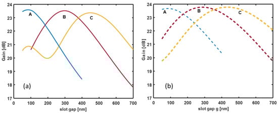
Figure 5.
Maximum gain for (a) the TE (solid curves) and (b) the TM (dashed curves) in the case of the three configurations A (w = 600 nm), B (w = 900 nm), and C (w = 1100 nm). In all the considered cases, the gain maximum occurs at Φ = 0 and θ = π/2. The antenna length is La = 25 μm, and the wavelength is λ = 1.55 µm.
From Figure 5a,b, we can infer that the gap value g can be suitably chosen to achieve the maximum gain for both the TE and TM polarizations. With reference to the three configurations A, B, and C, the maximum gain values for both the polarizations correspond to g = 100 nm, g = 300 nm, and g = 500 nm, respectively. For these three gap values, the maximum gain difference between the two polarizations is minimized, and it is less than 0.4 dB.
A further performance indicator for the proposed Vivaldi antenna is the power reflection coefficient |S11|2 at the input strip waveguide. The Vivaldi antenna is a single port device with negligible dielectric losses. Therefore, if the back reflection at the input port is low, most of the input power is coupled from the strip waveguide to the Vivaldi antenna, and then, it is radiated in the surrounding space. Figure 6 shows the power reflection coefficient |S11|2 calculated at the input port for the TE (solid curve) and TM (dashed curves) modes as a function of the initial slot gap value g. The blue, red, and yellow curves correspond to the configurations A (w = 600 nm), B (w = 900 nm), and C (w = 1100 nm), respectively.
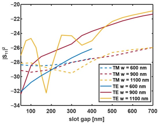
Figure 6.
Power reflection coefficient |S11|2 calculated at the input port for the TE (solid curve) and TM modes (dashed curves) as a function of the initial slot gap value g. The blue, red, and yellow curves correspond to configurations A (w = 600 nm), B (w = 900 nm), and C (w = 1100 nm), respectively. For each value of the slot gap g, the slot rail width s can be calculated from the formula s = (w −g)/2. The wavelength is λ = 1.55 µm.
The curves in Figure 6 take into account both the power coupling between the strip and the slot waveguide and the radiation in the surrounding medium. Because the |S11|2 coefficient is less than −21 dB for all the considered cases, the power is efficiently coupled from the strip waveguide to the Vivaldi antenna coherently with the mode overlap integral in Figure 2.
By considering the gain curves in Figure 5, we can say that, given a certain strip width w, the gap g can be optimized to maximize the gain. Once the antenna cross section has been optimized, another geometrical parameter that influences the achievable antenna gain is the length La of the Vivaldi radiator. As an example, Figure 7 shows the maximum gain as a function of the antenna length La for the TE (solid curve) and the TM (dashed curve) modes, in the case of configuration B (w = 900 nm) with slot gap g = 300 nm and slot rail width s = 300 nm. The results of the other configurations are not reported to avoid redundancies.
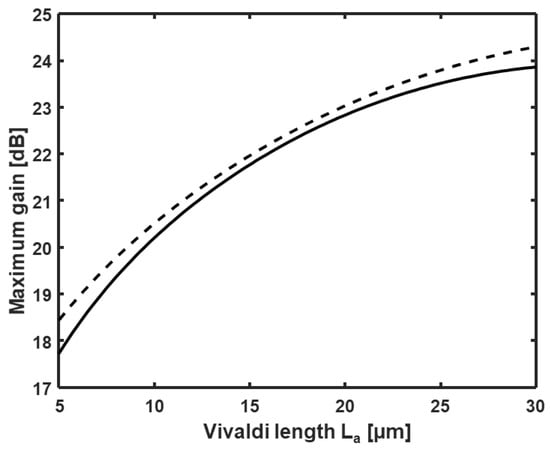
Figure 7.
Maximum gain as a function of the antenna length La for the TE (solid curve) and the TM (dashed curve) modes, in the case of configuration B (w = 900 nm) with slot gap g = 300 nm and slot rail width s = 300 nm. The wavelength is λ = 1.55 µm.
As can be seen from Figure 7, the gain increases with the length of the antenna for both the TE and the TM polarizations. Moreover, the gain values for the two polarizations are very close (less than 0.4 dB difference), thus showing that the polarization-insensitive behavior of the gain is preserved also for the different lengths of the Vivaldi radiator. Similar behavior is obtained also for the A and C configurations.
The results discussed above, which refer to 3D-FDTD simulations of the dielectric Vivaldi antenna surrounded by a homogeneous SiO2 medium, are useful for defining the design criteria of the antenna and for identifying those configurations that show similar radiation characteristics, which are expressed in terms of gain, for both the TE and the TM polarizations. This makes it possible to study the TE and TM propagation in on-chip point-to-point wireless links with the same antenna gain. According to the well-known Friis transmission equation, when the wireless communication takes place in homogeneous medium, the received power is related to the antenna gain of the transmitter and of the receiver. Therefore, the same received power is estimated, in homogeneous medium, for both the TE and TM polarizations in point-to-point links between two integrated Vivaldi antennas.
However, the on-chip wireless communication occurs in a multilayer structure, which is typical of photonic integrated circuits. As will be discussed in the following, when the propagation occurs in a multilayer medium, the power budget of the point-to-point link is found to be different for the two polarizations, even if the antenna gain is the same. This difference can be ascribed to the radiated wave polarization and to the interaction of the radiated field with the multilayer medium.
3. Wireless Propagation in On-Chip Multilayer Structure with TE and TM Polarizations
For the analysis of the point-to-point on-chip wireless links between two Vivaldi antennas, the multilayer structure shown in Figure 8 was considered in the 3D-FDTD numerical model: (a) yz cross-section and (b) xz cross-section. The multilayer shown in Figure 8 corresponds to commercially available SiN samples with a bottom layer of bulk Si, an overlying layer of SiO2 of height , and a further layer of SiN of thickness , housing the standard waveguides and the Vivaldi antennas. The antenna layer is then covered with a polymer-based cladding layer. The topmost layer, i.e., air, and the bottom one, i.e., bulk Si, were modeled as infinite in the simulations through Perfectly Matched Layer (PML) boundary conditions. The PML conditions were also applied on all the edges of the computational domain.
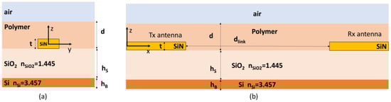
Figure 8.
Scheme of the on-chip multilayered structure: (a) yz cross-section, and (b) xz cross-section.
As numerically and experimentally investigated by the authors in [30,36,37,38] for SOI-based on-chip wireless links, the electromagnetic waves that propagate in the on-chip multilayer structure experience multiple reflections and transmissions at the medium discontinuities. The consequent multipath interference can be constructive or destructive, resulting in increased or fading received signal. Differently from this work, in [37], links between simple taper antennas, which were obtained by tapering standard SOI waveguides, were analyzed, and only the TE polarization was considered for signal excitation.
It is worth pointing out that the behavior of the wireless optical signal in a multilayer medium is strongly dependent on the material characteristics, either in terms of refractive indices or in terms of layer thicknesses. These features imply that every specific multilayer structure must be carefully analyzed to improve the link performances.
To analyze the effect of the wave polarization on the link performances, different multilayer structures have been studied considering different thicknesses and different refractive indices of the cladding (polymer) layer. The cladding is usually introduced as a passivation layer in integrated optics, mainly to reduce scattering losses. Here, this layer plays another important role due to the presence of multiple reflections.
As a case of study, we considered the variation in the thickness of the polymer layer composed of poly-methyl-methacrylate (PMMA), which is characterized by a refractive index value (np = 1.4925) very near to that of SiO2 (nSiO2 = 1.445).
Here, we quantify the performances of the wireless point-to-point links by calculating the transmittance at the receiving (Rx) antenna, as the power coupled into the receiver waveguide divided by that in input at the transmitter (Tx). Figure 9a,b show the transmittances, which were calculated for the TE and the TM polarizations, respectively, as a function of the link distance dlink for different values d of the cladding layer thickness. The transmittances, which were obtained through a mode expansion monitor [45], are expressed in dB, and they represent the fraction of power coupled to the mode of the receiving waveguide by the corresponding antenna.
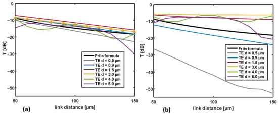
Figure 9.
Transmittance in dB, which is calculated at the receiver waveguide as a function of the link distance for different values of the PMMA top-layer thickness: (a) TE and (b) TM polarizations. The black curves denote the transmittance calculated by the Friis transmission equation for a point-to-point link in a homogeneous medium (with refractive index nSiO2 = 1.445). The wavelength is λ = 1.55 µm.
For the sake of comparison, the transmittance at the Rx port for a point-to-point link in a homogeneous medium (with refractive index equal to nSiO2 = 1.445) was also calculated by the well-known Friis transmission equation [49]:
In Equation (5), PTx is the power in input to the transmitter waveguide, PRx is the power coupled to the receiver waveguide, GTx and GRx are the gains of the transmitting and of the receiving antenna (calculated, as before, when the antennas are immersed in a homogeneous SiO2 medium), λSiO2 is the wavelength in the propagation medium, and dlink is the link distance, i.e., the distance between the Rx and the Tx antennas. Friis-formula transmittance is also reported in Figure 9 for the TE and for the TM polarizations (black curves). Because the gain of the Vivaldi antenna is the same for the two polarizations, the curves calculated by the Friis transmission equation are equal for the TE and the TM propagations.
As we can see from Figure 9a, for the lowest considered value of the PMMA layer thickness, i.e., d = 0.5 μm, the transmittance T at the Rx waveguide (gray curve) is below the one pertaining to the Friis transmission equation (black curve). When the thickness d is increased, the effect of the propagation in the multilayer medium becomes advantageous because the received power is higher than that in the homogeneous medium. However, for d = 4 μm (green curve) and d = 6 μm (violet curve), oscillations are observed in the transmittance. These oscillations are typical of constructive and destructive interferences due to multipath propagation in multilayer media.
When the TM polarization is considered, as shown in Figure 9b, the effect of the variation in the thickness d is more pronounced. For d = 0.5 μm and d = 0.9 μm, the received power is lower than that in the homogeneous medium (black curve). However, by increasing the thickness d (i.e., d = 1.5 μm and d = 3 μm in the reported examples), a significant increase in the received power is achieved with respect to the propagation in the homogeneous medium. Moreover, in the case of the TM polarization, oscillations occur in the transmittance curves for the thickness values d = 4 μm (green curve) and d = 6 μm (violet curve).
Moreover, by comparing Figure 9a,b, we can see that a significant increase in the transmittance occurs for the larger values of the thickness d in the case of the TM polarization. As an example, for dlink = 150 µm and d = 3 µm, the transmittances are T = −16.8 dB and T = −6.2 dB for the TE and the TM polarizations, respectively.
In the on-chip multilayer structure, the optical wireless communication is influenced by the antenna radiation diagram, by the thicknesses and refractive indices of the layers, and by the wave polarization.
The dominant electromagnetic field components of the waves radiated by the Vivaldi antenna are different for the two polarizations. In particular, EΦ and Hθ are the dominant components for the TE polarization, whereas Eθ and HΦ are the dominant ones for the TM polarization. Therefore, when the fundamental TE mode is given in input to the transmitting antenna, the radiated electromagnetic field can be considered to be s-polarized with respect to the multilayer interfaces, being the electric field EΦ parallel to the interfaces. Similarly, the TM mode gives a p-polarized electromagnetic field. The different behavior of the TE- and the TM-polarized waves is, therefore, associated to the different boundary conditions at the interfaces and to the different Fresnel coefficients.
To better understand the results reported in Figure 9, Figure 10 shows the normalized electric field amplitude (in logarithmic scale) calculated in the xz-vertical plane for y = 0 μm (i.e., in the middle of the antennas), for the TE polarization. The link distance is dlink = 100 μm, and different values of the thickness d are considered, namely: (a) d = 0.5 μm, (b) d = 0.9 μm, (c) d = 3 μm, and (d) d = 4 μm. The antennas and the multilayer interfaces are denoted by the black lines.
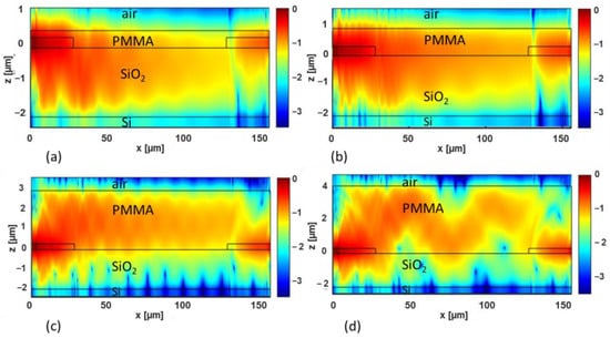
Figure 10.
Normalized electric field (in logarithmic scale) calculated in the xz-vertical plane for y = 0 μm (i.e., in the middle of the antennas) for the TE polarization. The link distance is dlink = 100 μm and different values of the thickness d are considered, namely: (a) d = 0.5 μm, (b) d = 0.9 μm, (c) d = 3 μm, and (d) d = 4 μm. The antennas and the multilayer interfaces are denoted by the black lines. The wavelength is λ = 1.55 µm.
Considering Figure 10, in the TE case of d = 0.5 μm, the field tends to concentrate in the substrate (SiO2) layer, and it experiences a decay while propagating from the Tx to the Rx antenna because it is partly transmitted in the Si bulk substrate and in the air overlayer. Therefore, the Rx antenna can collect only a small part of the overall electromagnetic field. When d = 0.9 μm (Figure 10b), the field tends to concentrate more in the cladding layer (PMMA), and it is received more efficiently by the Rx antenna. This guiding effect in the PMMA layer becomes more apparent in the case of d = 3 μm (Figure 10c). In the case of d = 4 μm (Figure 10d), we can still consider the field to be mainly confined in the PMMA cladding, but an interference pattern is clearly visible, which explains the oscillations of the transmittance (green curve in Figure 9a) as a function of the link distance.
Similarly, Figure 11 shows the electric field pattern calculated via 3D-FDTD simulations in the xz plane for y = 0 μm (i.e., in the middle of the antennas) for the TM polarization and for a fixed link distance dlink = 100 μm. Furthermore, in this case, different values of the thickness d are considered, namely: (a) d = 0.5 μm, (b) d = 0.9 μm, (c) d = 3 μm, and (d) d = 4 μm.
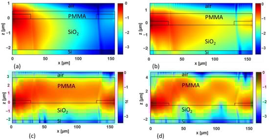
Figure 11.
Normalized electric field (in logarithmic scale) calculated in the xz-vertical plane for y = 0 μm (i.e., in the middle of the antennas), for the TM polarization. The link distance is dlink = 100 μm, and different values of the thickness d are considered, namely: (a) d = 0.5 μm, (b) d = 0.9 μm, (c) d = 3 μm, and (d) d = 4 μm. The antennas and the multilayer interfaces are denoted by the black lines. The wavelength is λ = 1.55 µm.
In Figure 11a,b, it is apparent that the field is strongly attenuated due to the prevalent radiation toward the Si bulk layer, for both d = 0.5 μm and d = 0.9 μm. When the thickness d is increased, the electromagnetic field tends to concentrate in the PMMA layer, giving rise to a guiding effect. In fact, when d = 3 μm (Figure 11c), the field appears to be well confined in the PMMA layer. Moreover, the oscillations due to the multiple reflections and transmissions at the interfaces are less pronounced with respect to the TE case (see Figure 10c). Additionally, for the TM polarization, in the case of d = 4 μm (Figure 11d), the field is confined mainly in the PMMA cladding, but an interference pattern is clearly visible in agreement with the oscillations of the transmittance as a function of the link distance (green curve in Figure 9b).
For the sake of completeness, Figure 12 and Figure 13 show, for the TE and for the TM polarizations, respectively, the electric field calculated via the 3D-FDTD simulation in the xy-horizontal plane for z = 0 μm (i.e., in the middle of the antennas), for a fixed link distance dlink = 100 μm. Different values of the thickness d are considered, namely: (a) d = 0.5 μm, (b) d = 0.9 μm, (c) d = 3 μm, and (d) d = 4 μm. The solid lines denote the geometry of the antennas, and the color bar represents the normalized amplitude of the electric field in logarithmic scale.
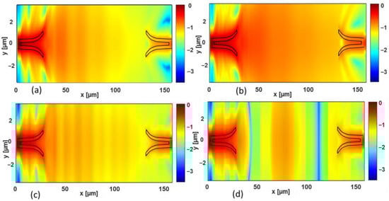
Figure 12.
Normalized electric field (in logarithmic scale) calculated in the xy-vertical plane for z = 0 μm (i.e., in the middle of the antennas) for the TE polarization. The link distance is dlink = 100 μm, and different values of the thickness d are considered, namely: (a) d = 0.5 μm, (b) d = 0.9 μm, (c) d = 3 μm, and (d) d = 4 μm. The antennas are denoted by the black lines. The wavelength is λ = 1.55 µm.
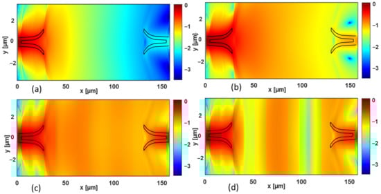
Figure 13.
Normalized electric field (in logarithmic scale) calculated in the xy-vertical plane for z = 0 μm (i.e., in the middle of the antennas) for the TM polarization. The link distance is dlink = 100 μm, and different values of the thickness d are considered, namely: (a) d = 0.5 μm, (b) d = 0.9 μm, (c) d = 3 μm, and (d) d = 4 μm. The antennas are denoted by the black lines. The wavelength is λ = 1.55 µm.
In the case of TE polarization (Figure 12), the electromagnetic field spreads in the xy-horizontal plane around the transmitting antenna, and it couples at the receiving one, as expected for a point-to-point wireless link. Owing to the presence of the multilayer structure, oscillations appear in the xy-plane field distributions, especially in the case of d = 4 µm (Figure 12d), where an interference pattern is apparent.
In the case of the TM polarization, when the cladding thickness is d = 0.5 µm (Figure 13a), the electromagnetic field rapidly decays due to the dominant radiation towards the bulk layer (see Figure 11a for comparison). For larger thicknesses, i.e., Figure 13b–d, the electromagnetic field spreads around the transmitting antenna and reaches the receiving one. Some oscillations in the field pattern are present due to the multipath interference, but the contribution of the destructive interference is less pronounced than in the TE case.
As mentioned before, the dominant electromagnetic field components of the radiated waves are different for the two polarizations. In particular, EΦ and Hθ are the dominant components for the TE polarization, whereas Eθ and HΦ are the dominant ones for the TM polarization.
The electromagnetic propagation in the multilayer structure can be regarded as the superposition of multiple reflected and transmitted rays at the different interfaces (e.g., silicon–silica, silica–polymer, polymer–air interfaces), each characterized by different Fresnel coefficients. The effect of the multipath propagation is, therefore, different for the two polarizations, given that the Fresnel coefficients are different. In particular, when the cladding thickness is small, the recombination of the multiple rays is, in general, destructive in the cladding layer, and the field tends to be radiated toward the Si bulk layer. Therefore, the transmittance at the receiving antenna is lower than that in free space.
When the cladding thickness is increased, the point-to-point link in the multilayer shows an increased transmittance with respect to that in free space, especially in the case of TM polarization. This is due to an almost guiding effect that occurs in the overlayer, where the multipath composition is, in general, constructive. The increase in the transmittance and its dependence on the cladding thickness are more pronounced for the TM case because of the different Fresnel coefficients in the multipath propagation.
Another degree of freedom in the analysis of on-chip wireless communication is the cladding refractive index. Figure 14a,b show for the TE and the TM polarizations, respectively, the transmittance calculated as a function of the link distance for different cladding refractive indices. As can be seen in Figure 14, the variation in the cladding refractive index does not significantly change the transmittance for the TE polarization (Figure 14a). For the TM polarization, the transmittance at the receiving waveguide is almost the same for nclad = 1.492 and for nclad = 1.592, whereas it is lower when the cladding refractive index is equal to that of the SiO2 substrate (red dashed curve of Figure 14b).
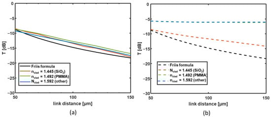
Figure 14.
Transmittance in dB, which is calculated at the receiver waveguide as a function of the link distance for different values of the cladding refractive index: (a) TE and (b) TM polarizations. The black curves denote the transmittance calculated by the Friis transmission equation for a point-to-point link in a homogeneous medium (with refractive index nSiO2 = 1.445). The cladding thickness is d = 3 µm, and the wavelength is λ = 1.55 µm.
The proposed Vivaldi antenna is a non-resonant structure, and it can allow broadband communication between two nodes in an optical network on chip. As an example, Figure 15 shows the transmittance calculated at the receiving antenna as a function of the wavelength, for the TE (solid curve) and the TM (dashed curves) polarizations. In this case, the link distance is dlink = 100 µm, and the PMMA is considered to be a cladding polymer (thickness d = 3 µm) in the multilayer structure. As Figure 15 shows, the transmittance is almost constant with the wavelength (variation in less than 0.6 dB for both the polarizations), covering the entire C-band. Given the broadband behavior, the proposed antenna is suitable for the implementation of WDM schemes in on-chip communication.
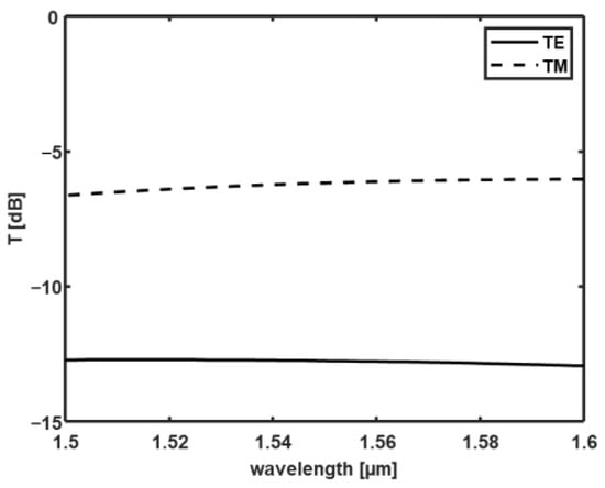
Figure 15.
Transmittance in dB, which is calculated at the receiver waveguide as a function of wavelength for the TE (solid curve) and the TM (dashed curves) polarizations. The link distance is dlink = 100 µm, and a multilayer structure with PMMA as cladding polymer and cladding thickness d = 3 µm is considered.
Given the higher transmittance for the TM polarization with respect to the TE one, the overall performance on the point-to-point link can be significantly improved by selecting the TM mode in input to the transmitting antenna. This opens new possibilities for the design of on-chip optical wireless interconnection networks, provided that the polarization selection is implemented at the input of the waveguide feeding the antenna (e.g., through TM grating couplers or polarization rotators).
4. Conclusions
An integrated dielectric Vivaldi antenna has been proposed for point-to-point on-chip communication links. The antenna is constructed with a SiN slot waveguide tapered according to a Vivaldi profile, and it is directly coupled to an input SiN strip waveguide. The design criteria to optimize the antenna gain are defined in relation to the geometrical parameters of the Vivaldi-shaped slot waveguide and to the antenna length. The designed antenna exhibits the same high gain for both the TE and TM polarizations, (i.e., 23.8 dB and 23.52 dB for the TE and the TM modes, respectively).
The analysis of point-to-point communication links between two Vivaldi antennas has been reported by considering the electromagnetic propagation in on-chip multilayer structures, with different thicknesses and different refractive indices of the cladding layer. It has been shown that, when the antennas are fed with TM-polarized modes, lower propagation losses are achieved.
Given that the Vivaldi antenna is a non-resonant structure, it can allow broadband communication between two nodes in OWiNoCs, thus allowing the implementation of WDM schemes in on-chip communication.
Author Contributions
Conceptualization: G.C., G.B., F.F., M.B., V.T. and V.P. Methodology: G.C., G.B., F.F., M.B., V.T. and V.P. Software: G.C. and G.B. Validation: G.C., G.B., F.F., M.B., V.T. and V.P. Investigation: G.C., G.B., F.F., M.B., V.T. and V.P. Data curation: G.C., G.B., F.F., M.B., V.T. and V.P. Writing—original draft preparation, G.C., G.B., F.F., M.B., V.T. and V.P. Writing—review and editing: G.C., G.B., F.F., M.B., V.T. and V.P. Supervision: G.C. All authors have read and agreed to the published version of the manuscript.
Funding
This work was partly supported by the “IMPACT” project, funded by the Apulia region under the call “Progetti di ricerca scientifica innovativi di elevato standard internazionale (art. 22 della legge regionale 30 November 2019, n. 52)”, by the project “Integrated Magneto-Biplasmonic Circulator For Silicon Platform (IMPACTS)”, funded under the call Galileo 2022/ Galilée 2022, and by the European Union under the Italian National Recovery and Resilience Plan (NRRP) of NextGenerationEU, partnership on “Telecommunications of the Future” (PE00000001—program “RESTART”).
Institutional Review Board Statement
Not applicable.
Informed Consent Statement
Not applicable.
Data Availability Statement
The data that support the findings of this study are available from the corresponding author upon reasonable request.
Conflicts of Interest
The authors declare no conflict of interest.
References
- Flich, J.; Bertozzi, D. Designing Network-on-Chip Architectures in the Nanoscale Era; CRC Press: Boca Raton, FL, USA, 2019. [Google Scholar]
- Nychis, G.; Fallin, C.; Moscibroda, T.; Mutlu, O.; Sesharr, S. On-chip networks from a networking perspective: Congestion and scalability in many-core interconnects. Comput. Commun. Rev. 2012, 42, 407–418. [Google Scholar] [CrossRef]
- Zia, M.; Wan, C.; Zhang, Y.; Bakir, M. Electrical and photonic off-chip interconnection and system integration. In Optical Interconnects for Data Centers; Woodhead Publishing: Cambridge, UK, 2017; pp. 265–286. [Google Scholar]
- Shacham, A.; Bergman, K.; Carloni, L.P. On the design of a photonic network-on-chip. In Proceedings of the 1st International Symposium on Networks-on-Chip (NOCS’07), Princeton, NJ, USA, 7–9 May 2007; pp. 53–64. [Google Scholar]
- Terzenidis, N.; Moralis-Pegios, M.; Pitris, S.; Mourgias-Alexandris, G.; Mitsolidou, C.; Fotiadis, K.; Vyrsokinos, K.; Alexoudi, T.; Pleros, N. Board- and rack-scale optical interconnection architectures for disaggregated data centers. In Proceedings of the SPIE, Optical Interconnects XX, San Francisco, CA, USA, 4–6 February 2020; p. 1128606. [Google Scholar]
- Deb, S.; Mondal, H.K. Wireless network-on-chip: A new era in multi-core chip design. In Proceedings of the 25th IEEE International Symposium on Rapid System Prototyping, New Delhi, India, 16–17 October 2014; pp. 59–64. [Google Scholar]
- Mirza, A.; Sunny, F.; Walsh, P.; Hassan, K.; Pasricha, S.; Nikdast, M. Silicon Photonic Microring Resonators: A Comprehensive Design-Space Exploration and Optimization Under Fabrication-Process Variations. IEEE Trans. Comput. Aided Des. Integr. Circuits Syst. 2022, 41, 3359–3372. [Google Scholar] [CrossRef]
- Calò, G.; Alexandropoulos, D.; Petruzzelli, V. Active WDM filter on dilute nitride quantum well photonic band gap waveguide. Prog. Electromagn. Res. Lett. 2012, 35, 37–49. [Google Scholar] [CrossRef]
- Abadian, S.; Magno, G.; Yam, V.; Dagens, B. Broad-band plasmonic isolator compatible with low-gyrotropy magneto-optical material. Opt. Express 2021, 29, 4091–4104. [Google Scholar] [CrossRef]
- Calò, G.; Alexandropoulos, D.; Petruzzelli, V. Active photonic band-gap switch based on GalnNAs multiquantum well. IEEE Photonics J. 2012, 4, 1936–1946. [Google Scholar] [CrossRef]
- Truppel, A.; Tseng, T.M.; Bertozzi, D.; Alves, J.C.; Schlichtmann, U. PSION+: Combining Logical Topology and Physical Layout Optimization for Wavelength-Routed ONoCs. IEEE Trans. Comput. Aided Des. Integr. Circuits Syst. 2020, 39, 5197–5210. [Google Scholar] [CrossRef]
- Thonnart, Y.; Bernabe, S.; Charbonnier, J.; Bernard, C.; Coriat, D.; Fuguet, C.; Tissier, P.; Charbonnier, B.; Malhouitre, S.; Saint-Patrice, D.; et al. POPSTAR: A Robust Modular Optical NoC Architecture for Chiplet-based3D Integrated Systems. In Proceedings of the 2020 Design, Automation and Test in Europe Conference and Exhibition (DATE), Grenoble, France, 9–13 March 2020; pp. 1456–1461. [Google Scholar]
- Lu, L.; Zhao, S.; Zhou, L.; Li, D.; Li, Z.; Wang, M.; Li, X.; Chen, J. 16 × 16 non-blocking silicon optical switch based on electro-optic Mach-Zehnder interferometers. Opt. Express 2016, 24, 9295–9307. [Google Scholar] [CrossRef]
- Calò, G.; D’Orazio, A.; Grande, M.; Marrocco, V.; Petruzzelli, V. Active InGaAsP/InP photonic bandgap waveguides for wavelength-selective switching. IEEE J. Quantum Electron. 2011, 47, 172–181. [Google Scholar] [CrossRef]
- Thirumaran, S.; Dhanabalan, S.S.; Sannasi, I.G. Design and analysis of photonic crystal ring resonator based 6 × 6 wavelength router for photonic integrated circuits. IET Optoelectron. 2021, 15, 40–47. [Google Scholar] [CrossRef]
- Calò, G.; Mescia, L.; Petruzzelli, V.; Prudenzano, F. Study of gain in photonic bandgap active InP waveguides. J. Opt. Soc. Am. B Opt. Phys. 2009, 26, 2414–2422. [Google Scholar] [CrossRef]
- Calò, G.; Alexandropoulos, D.; D’Orazio, A.; Petruzzelli, V. Wavelength selective switching in dilute nitrides multi quantum well photonic band gap waveguides. Phys. Status Solidi B Basic Res. 2011, 248, 1212–1215. [Google Scholar] [CrossRef]
- Kazmierczak, A.; Bogaerts, W.; Drouard, E.; Dortu, F.; Rojo-Romeo, P.; Gaffiot, F.; Van Thourhout, D.; Giannone, D. Highly integrated optical 4 x 4 crossbar in silicon-on-insulator technology. J. Lightw. Technol. 2009, 27, 3317–3323. [Google Scholar] [CrossRef]
- Sherwood-Droz, N.; Sherwood-Droz, N.; Wang, H.; Chen, L.; Lee, B.G.; Biberman, A.; Bergman, K.; Lipson, M. Optical 4 × 4 hitless silicon router for optical Networks-on-Chip (NoC). Opt. Express 2008, 16, 15915–15922. [Google Scholar] [CrossRef] [PubMed]
- Cheng, Q.; Bahadori, M.; Hung, Y.H.; Huang, Y.; Abrams, N.; Bergman, K. Scalable microring-based silicon Clos switch fabric with switch-and-select stages. IEEE J. Sel. Top. Quantum Electron. 2019, 25, 1–11. [Google Scholar] [CrossRef]
- Lu, L.; Zhou, L.; Li, Z.; Li, X.; Chen, J. Broadband 4 × 4 Nonblocking Silicon Electrooptic Switches Based on Mach–Zehnder Interferometers. IEEE Photonics J. 2015, 7, 1–8. [Google Scholar] [CrossRef]
- Lemic, F.; Abadal, S.; Tavernier, W.; Stroobant, P.; Colle, D.; Alarcon, E.; Marquez-Barja, J.; Famaey, J. Survey on Terahertz Nanocommunication and Networking: A Top-Down Perspective. IEEE J. Sel. Areas Commun. 2021, 39, 1506–1543. [Google Scholar] [CrossRef]
- Imani, F.; Abadal, S.; del Hougne, P. Metasurface-Programmable Wireless Network-On-Chip. Adv. Sci. 2022, 9, 2201458. [Google Scholar] [CrossRef]
- Abadal, S.; Mestres, A.; Torrellas, J.; Alarcon, E.; Cabellos-Aparicio, A. Medium Access Control in Wireless Network-on-Chip: A Context Analysis. IEEE Commun. Mag. 2018, 56, 172–178. [Google Scholar] [CrossRef]
- Abadal, S.; Hosseininejad, S.E.; Cabellos-Aparicio, A.; Alarcón, E. Graphene-Based terahertz antennas for area-constrained applications. In Proceedings of the 40th International Conference on Telecommunications and Signal Processing (TSP), Barcelona, Spain, 5–7 July 2017; pp. 817–820. [Google Scholar]
- Alù, A.; Engheta, N. Wireless at the nanoscale: Optical interconnects using matched nanoantennas. Phys. Rev. Lett. 2010, 104, 213902. [Google Scholar] [CrossRef] [PubMed]
- Yang, Y.; Li, Q.; Qiu, M. Broadband nanophotonic wireless links and networks using on-chip integrated plasmonic antennas. Sci. Rep. 2016, 6, 19490. [Google Scholar] [CrossRef] [PubMed]
- Merlo, J.M.; Nesbitt, N.T.; Calm, Y.M.; Rose, A.H.; D’Imperio, L.; Yang, C.; Naughton, J.R.; Burns, M.J.; Kempa, K.; Naughton, M.J. Wireless communication system via nanoscale plasmonic antennas. Sci. Rep. 2016, 6, 31710. [Google Scholar] [CrossRef] [PubMed]
- García-Meca, C.; Lechago, S.; Brimont, A.; Griol, A.; Mas, S.; Sánchez, L.; Bellieres, L.; Losilla, N.S.; Martí, J. On-chip wireless silicon photonics: From reconfigurable interconnects to lab-on-chip devices. Light Sci. Appl. 2017, 6, e17053. [Google Scholar] [CrossRef] [PubMed]
- Badrul, A.; Calò, G.; Bellanca, G.; Nanni, J.; Kaplan, A.E.; Barbiroli, M.; Fuschini, F.; Bassi, P.; Dehkordi, J.S.; Tralli, V.; et al. Numerical and experimental analysis of on-chip optical wireless links in presence of obstacles. IEEE Photonics J. 2020, 13, 1–11. [Google Scholar]
- Kraus, J.D. Antennas, 2nd ed.; McGraw-Hill: New York, NY, USA, 1988. [Google Scholar]
- Ghanim, A.M.; Hussein, M.; Hameed, M.F.O.; Yahia, A.; Obayya, S.S.A. Highly Directive Hybrid Yagi-Uda Nanoantenna for Radition Emission Enhancement. IEEE Photonics J. 2016, 8, 7585107. [Google Scholar] [CrossRef]
- Damasceno, G.H.B.; Carvalho, W.O.F.; Mejía-Salazar, J.R. Design of Plasmonic Yagi–Uda Nanoantennas for Chip-Scale Optical Wireless Communications. Sensors 2022, 22, 7336. [Google Scholar] [CrossRef]
- Bellanca, G.; Calò, G.; Kaplan, A.E.; Bassi, P.; Petruzzelli, V. Integrated Vivaldi plasmonic antenna for wireless on-chip optical communications. Opt. Express 2017, 25, 16214–16227. [Google Scholar] [CrossRef] [PubMed]
- Calò, G.; Bellanca, G.; Alam, B.; Kaplan, A.E.; Bassi, P.; Petruzzelli, V. Array of plasmonic Vivaldi antennas coupled to silicon waveguides for wireless networks through on-chip optical technology—WiNOT. Opt. Express 2018, 26, 30267–30277. [Google Scholar] [CrossRef]
- Fuschini, F.; Barbiroli, M.; Calò, G.; Tralli, V.; Bellanca, G.; Zoli, M.; Dehkordi, J.S.; Nanni, J.; Alam, B.; Petruzzelli, V. Multi-Level Analysis of On-Chip Optical Wireless Links. Appl. Sci. 2020, 10, 196. [Google Scholar] [CrossRef]
- Nanni, J.; Bellanca, G.; Calò, G.; Badrul, A.; Kaplan, E.; Barbiroli, M.; Fuschini, F.; Dehkordi, J.S.; Tralli, V.; Bassi, P.; et al. Multi-path propagation in on-chip optical wireless links. IEEE Photonics Technol. Lett. 2020, 32, 1101–1104. [Google Scholar] [CrossRef]
- Fuschini, F.; Barbiroli, M.; Zoli, M.; Bellanca, G.; Calò, G.; Bassi, P.; Petruzzelli, V. Ray tracing modeling of electromagnetic propagation for on-chip wireless optical communications. J. Low Power Electron. Appl. 2018, 8, 39. [Google Scholar] [CrossRef]
- Zhang, Y.; He, Y.; Zhu, Q.; Jiang, X.; Guo, X.; Qiu, C.; Su, Y. On-chip silicon polarization and mode handling devices. Front. Optoelectron. 2018, 11, 77–91. [Google Scholar] [CrossRef]
- Cheng, L.; Mao, S.; Li, Z.; Han, Y.; Fu, H.Y. Grating couplers on silicon photonics: Design principles, emerging trends and practical issues. Micromachines 2020, 11, 666. [Google Scholar] [CrossRef]
- Georgieva, G.; Voigt, K.; Peczek, A.; Mai, C.; Zimmermann, L. Design and performance analysis of integrated focusing grating couplers for the transverse-magnetic TM00 mode in a photonic BiCMOS technology. J. Eur. Opt. Soc. 2020, 16, 7. [Google Scholar] [CrossRef]
- Doerr, C.R.; Chen, L.; Chen, Y.-K.; Buhl, L.L. Wide bandwidth silicon nitride grating coupler. IEEE Photonics Technol. Lett. 2010, 22, 1461–1463. [Google Scholar] [CrossRef]
- Gallacher, K.; Griffin, P.F.; Riis, E.; Sorel, M.; Paul, D.J. Silicon nitride waveguide polarization rotator and polarization beam splitter for chip-scale atomic systems. APL Photonics 2022, 7, 046101. [Google Scholar] [CrossRef]
- Zhang, J.; Yu, M.; Lo, G.-Q.; Kwong, D.-L. Silicon-waveguide-based mode evolution polarization rotator. IEEE J. Sel. Top. Quantum Electron. 2010, 16, 53–60. [Google Scholar] [CrossRef]
- Lumerical Solutions, Inc. Available online: https://www.ansys.com/products/photonics (accessed on 15 December 2022).
- Philipp, H.R. Optical properties of silicon nitride. J. Electrochim. Soc. 1973, 120, 295–300. [Google Scholar] [CrossRef]
- Bååk, T. Silicon oxynitride; a material for GRIN optics. Appl. Opt. 1982, 21, 1069–1072. [Google Scholar] [CrossRef] [PubMed]
- Han, K.; Kim, S.; Wirth, J.; Teng, M.; Xuan, Y.; Niu, B.; Qi, M. Strip-slot direct mode coupler. Opt. Express 2016, 24, 6532–6541. [Google Scholar] [CrossRef] [PubMed]
- Collin, R.E. Antennas and Radiowave Propagation; McGraw-Hill: New York, NY, USA, 1985. [Google Scholar]


Disclaimer/Publisher’s Note: The statements, opinions and data contained in all publications are solely those of the individual author(s) and contributor(s) and not of MDPI and/or the editor(s). MDPI and/or the editor(s) disclaim responsibility for any injury to people or property resulting from any ideas, methods, instructions or products referred to in the content. |
© 2023 by the authors. Licensee MDPI, Basel, Switzerland. This article is an open access article distributed under the terms and conditions of the Creative Commons Attribution (CC BY) license (https://creativecommons.org/licenses/by/4.0/).