Abstract
Compressed Sensing (CS) has been applied to electrocardiogram monitoring in wireless sensor networks, but existing sampling and compression circuits consume too much hardware. This paper proposes a low-power and small-area sampling and compression circuit with an Analog-to-Digital Converter (ADC) and a CS module. The ADC adopts split capacitors to reduce hardware consumption and uses a calibration technique to decrease offset voltage. The CS module uses an approximate addition calculation for compression and stores the compressed data in pulsed latches. The proposed addition completes the accurate calculation of the high part and the approximate calculation of the low part. In a 55 nm CMOS process, the ADC has an area of 0.011 mm2 and a power consumption of 0.214 μW at 10 kHz. Compared with traditional design, the area and power consumption of the proposed CS module are reduced by 19.5% and 31.7%, respectively. The sampling and compression circuit area is 0.325 mm2, and the power consumption is 2.951 μW at 1.2 V and 100 kHz. The compressed data are reconstructed with a percentage root mean square difference of less than 2%. The results indicate that the proposed circuit has performance advantages of hardware consumption and reconstruction quality.
1. Introduction
Wireless Sensor Networks (WSNs) [1] have been widely used in Electrocardiogram (ECG) monitoring by deploying sensor nodes to collect the sensing data. WSNs are limited by their battery, so reducing the power consumption of data acquisition and transmission can effectively extend their lives [2]. Compressed Sensing (CS) [3,4,5] is a sparse signal-based compression and reconstruction algorithm, affording a simple compression process and high reconstruction performance. ECG signal processing based on the CS algorithm mainly includes converting the acquired original signal into a digital signal for compression and then transmitting them wirelessly to the remote server for reconstruction. To ensure the reconstruction quality, an Analog-to-Digital Converter (ADC) [6] is critical and must meet the requirements of the compression process.
The ECG signal sampling and compression processes rely on analog and digital circuits. The analog circuit implementation is called the Analog-to-Information Converter (AIC). Saliga et al. [7] designed an AIC with random interval integration, integrating the input signal by a random reconfigurable integrator before the AD conversion. The random interval integration was a simple hardware implementation with commonly used components. Sadasivuni et al. [8] presented an AIC technique that utilized analog hyper-dimensional computing based on a reservoir-computing paradigm to ECG signal locally in-sensor and reduced radio frequency transmission by more than three orders of magnitude. Qian et al. [9] proposed a generalized AIC framework, which removed the model error between an analog signal and its equivalent discrete samples through the joint optimization for the discretization operator and its analysis sparse operator. The digital circuit compresses data after the ADC converts the ECG signal. Chen et al. [10] proposed a general sampling and compression architecture and evaluated the performance of two implementation modes. The results highlighted that the digital circuit implementation had significant power consumption advantages. Kumar et al. [11] implemented a pipeline architecture for a sampling and compression circuit that processed data at high speed and bypassed the computation of unimportant input samples by a wake-up call, reducing the power consumption of the hardware. Pareschi et al. [12] adopted a new method to deal with the saturation problem during the CS compression calculation, where the corresponding circuit adapted the energy distribution of the input signal to maximize the information contained in the measurement. Liu et al. [13] presented a novel sampling and compression circuit that could simultaneously compress and encrypt data. The circuit had high compression efficiency while guaranteeing reconstruction quality, and the Compression Factor (CF) ranged from 2 to 16.
In the existing ECG sampling and compression circuits, two problems lead to excessive hardware consumption. One is that the power consumption of ADC is relatively high, and some circuits employ external ADC causing unnecessary waste of resources due to functional redundancy. The other is that matrix compression adopts accurate calculation, and the compressed data are stored in registers imposing significant area and power consumption. Since CS is a lossy algorithm and considering an ECG signal, as long as the Percentage Root Mean Square Difference (PRD) of the reconstructed data is less than 9%, it can be used for medical diagnosis [14]. This paper proposes an ECG sampling and compression circuit consisting of a Successive Approximation Register Analog-to-Digital Converter (SAR ADC) for sampling and a CS module for compression. The CS module performs accurate and approximate calculations for the high and low parts of the ECG signal, respectively, based on the designed approximate addition calculation. Additionally, pulsed latches are used to store compressed data by optimizing the timing of the circuit.
This paper is structured as follows. In Section 2, the CS algorithm and the sampling and compression circuit are introduced and reviewed, and the problem of excessive hardware consumption in the existing circuits is pointed out. Section 3 presents the proposed scheme, and the sampling and compression circuit is designed based on the optimized ADC and CS module. The simulation results and circuit implementation are reported and discussed in Section 4. Finally, Section 5 provides the conclusion.
2. Sampling and Compression Circuit Based on Compressed Sensing
2.1. Compressed Sensing
CS is a sampling theory that compresses and reconstructs data based on signal sparsity [15]. The mathematical model of the CS algorithm is defined as Equation (1):
where X represents the N-dimensional original signal , Y is the M-dimensional compressed signal , and Φ denotes the M × N measurement matrix (M < N).
The measurement matrix largely determines the signal reconstruction quality. The measurement matrices commonly used in the CS algorithm are the Gaussian, Bernoulli, and binary. Considering the difficulty and consumption of hardware implementation, this paper utilizes a binary matrix as the measurement matrix, which converts the matrix multiplication and addition operations to selective addition operations [16], remapping the compression process into Equation (2):
The reconstruction process aims to find a definite and unique solution under certain constraints. Typical reconstruction algorithms are the Orthogonal Matching Pursuit, Compressed Sampling Matching Pursuit, and Block-Sparse Bayesian Learning (BSBL), with BSBL presenting a more stable and efficient reconstruction quality [17]. The performance of the CS algorithm is usually measured by CF and PRD metrics. CF is calculated in Equation (3):
where and are the numbers of bits of the original signal and compressed signal, respectively. A large CF represents high compression efficiency, and a small PRD indicates good reconstruction performance.
2.2. Sampling and Compression Circuit
Figure 1 illustrates the sensor node structure, mainly comprising a sensor module, data processing module, wireless communication module, and energy supply module. Specifically, the sensor samples, filters, and amplifies the sensing signal, and the ADC converts the analog signal into a digital signal. Once the data are processed, they are transmitted wirelessly. The sampling and compression circuit designed in this paper mainly involves the ADC and data processing module enclosed in the dotted box of Figure 1.
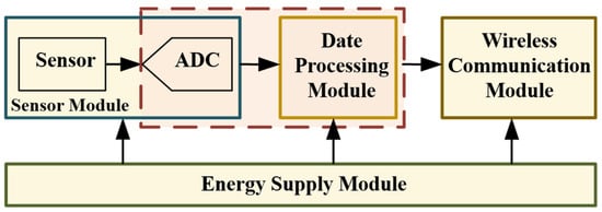
Figure 1.
The sensor node structure.
Given that ECG is a weak signal of low frequency and small amplitude, the sampled data are prone to distortion due to the influence of non-ideal factors in the circuit. Therefore, the performance of ADC directly affects the subsequent data processing and signal reconstruction. In this paper, we customize a SAR ADC with high accuracy and low power consumption, which can achieve a great adaptation with the data processing module.
The data processing module relies on the CS algorithm to compress the ECG signal. The compression and storage structure is depicted in Figure 2, where N original signals are added after being selected by the measurement matrix, and M adders work simultaneously. The compression register group stores the sum after each addition and feeds the stored value into the adder as an addend for the subsequent addition calculation. After each compression round, the storage register group stores and outputs the compressed results, and the stored data are not updated until the next compression round is completed. It should be noted that adders and registers are the main components of the compression and storage structure, so optimizing them can significantly reduce hardware consumption.
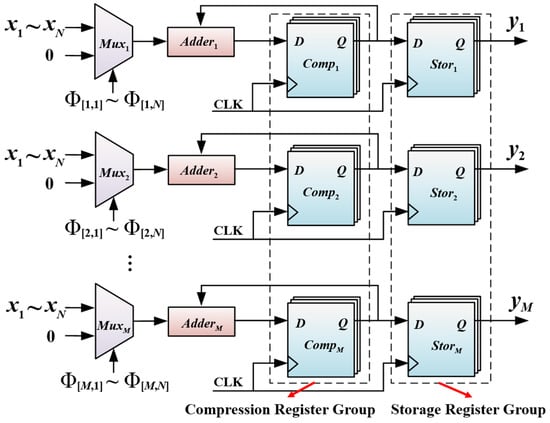
Figure 2.
The compression and storage structure.
3. Proposed Scheme
3.1. ADC
SAR ADC has the advantages of simple structure and low power consumption in medium and low-speed applications. Thus, a 12-bit SAR ADC is designed with the circuit structure illustrated in Figure 3. ADC is often inactive in the sampling and compression circuit, so an asynchronous format is adopted to avoid a high-frequency clock. The capacitor array and comparator are optimized to further reduce the area and power consumption and improve the data accuracy.
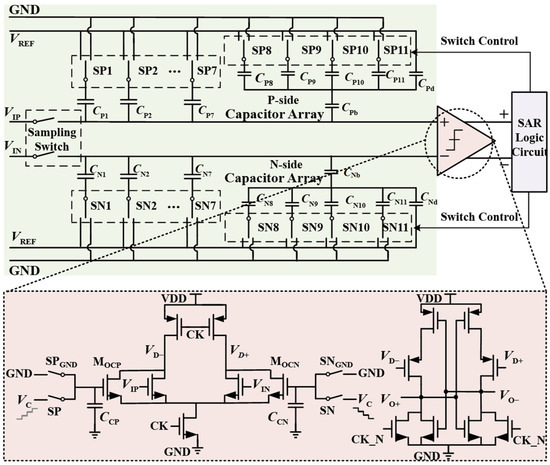
Figure 3.
The structure of SAR ADC.
The capacitor array can effectively avoid static power and only generate dynamic power when capacitors are switched. However, the area of the capacitor array increases significantly as accuracy improves. Therefore, this paper adopts the top plate sampling scheme and uses bridge capacitors CPb and CNb to divide the capacitor array into a split structure of high 8 bits and low 4 bits, reducing the number of capacitors from 4096 to 288 (92.97%). We choose the monotonic switching scheme, which can reduce the switching power by 81% compared with the traditional scheme [18], and is more suitable for the ECG sampling and compression circuit.
The Monte-Carlo simulation is performed to evaluate the influence of capacitor mismatch, and 100 simulations are completed for each capacitance value in the range of 7.02 fF to 21.53 fF. The simulation results are shown in Table 1, listing the corresponding Signal-to-Noise Ratio (SNR), Spurious Free Dynamic Range (SFDR), Effective Number of Bit (ENOB), and the standard deviation of ENOB for different capacitance values. The capacitance value is set to 15.59 fF based on the compromise of area and power consumption.

Table 1.
The simulation results of the influence of capacitor mismatch.
The comparator is the most critical analog module in SAR ADC, and this paper utilizes a bipolar dynamic latch comparator without static power consumption. Since the ECG signal is small and the offset of the existing comparator is typically in the order of tens of millivolts, low-value data can be lost. Therefore, during the pre-amplification stage, the calibration technique is used to reduce the offset voltage.
For a two-stage dynamic comparator, the offset voltage comprises a pre-amplification and latch stage offset. The offset voltage of the comparator can be expressed as Equation (4):
where VOS is the offset voltage of the comparator, VOSP and VOSL are the equivalent input offset voltage of the pre-amplification and latch stages, respectively, and A is the gain of the pre-amplification stage. The pre-amplifier stage offset is mainly caused by the mismatch of input transistor threshold voltage (VTH), width-to-length ratio (W/L), and load capacitance (CL) [19], as shown in Equation (5):
where , ΔVTH, ΔW/L, and ΔCL are threshold voltage mismatch, width-to-length ratio mismatch, and load capacitance mismatch, respectively, and AVT is the threshold voltage mismatch coefficient.
This paper adopts a digitally-assisted analog fine-tuning technique and places the auxiliary transistors MOCP and MOCN on both sides of the input pair transistors. By applying an unbalanced voltage to the gate of the auxiliary transistors, the current on the corresponding branch of the comparator is changed, thus reducing the influence of the MOS transistor offset.
At the beginning of calibration, the auxiliary transistors are reset first, connecting the gates of MOCP and MOCN to GND, and the differential inputs of the comparator input the same common-mode voltage. The comparator compares and outputs the results VO+ and VO− when the clock is switched to high. The calibration logic determines the connection position of the calibration voltage based on the first comparison output. Taking the first comparison results as and as an example, the calibration logic connects the gate of MOCN to the calibration voltage VC. As the step calibration voltage increases, the equivalent input offset voltage decreases. Until the outputs become and , the calibration logic disconnects the calibration voltage VC and the gate of MOCN to end the calibration, and the calibration voltage is maintained in the capacitor CCN.
3.2. CS Module
3.2.1. Addition
The binary matrix converts the compression process into a selective addition operation. We design an approximate addition calculation to improve circuit performance by sacrificing a little accuracy, as illustrated in Figure 4. We approximate the n-bit addend selected by the measurement matrix. The high (nm) bits of the addend remain unchanged, and the low m bits are approximated while a carry is generated.
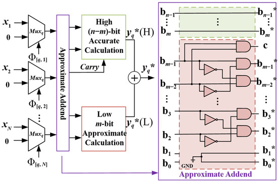
Figure 4.
The approximate addition calculation.
The approximate addend is expressed by Equation (6):
The bits of the high and low parts in the approximate addend are not fixed, and the more bits of the low part, the larger the error. Therefore, the bits of the low part must be determined according to the accuracy requirements of the circuit. Considering the low 4 bits as an example, the generated approximate addend and corresponding error are reported in Table 2.
Table 2.
The approximate addend and corresponding error.
The mathematical expectation of the resulting error is 0.25, as calculated in Equation (7), which is too small to ignore for binary data.
Furthermore, the more weighted bits are calculated accurately, and the less weighted bits are calculated approximately. It can be seen from Table 2 that there are only three values for the low 4 bits after approximation, which are 0000, 1000, and 0100, with probabilities of 1/2, 1/4, and 1/4, respectively. Therefore, the approximate accumulation sum of the low 4 bits is as Equation (8):
The accurate calculation of the high part is realized in the CS module, and the approximate calculation of the low part is completed in the remote server. When two results are added, the compressed data are obtained.
3.2.2. Storage
The storage units include a register and latch, as depicted in Figure 5. The register typically comprises two levels of master and slave latches, with the input signal meeting the setup time and hold time, thus eliminating glitches and ensuring data accuracy. The primary latch can be used to store stable data. For this work, a fast clock pulse signal is set as the trigger condition of the pulsed latch by optimizing the circuit timing. By reducing the conducting time of the latch, the probability of generating glitches reduces, thus improving the accuracy of the stored data. Furthermore, the hardware consumption of the latch is about half the register, so using latches affords lower power consumption.
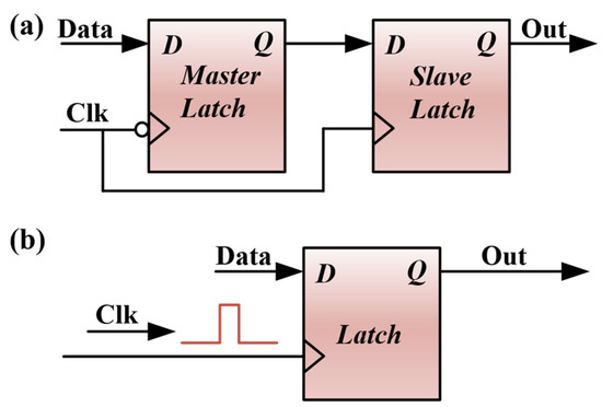
Figure 5.
The storage units: (a) master–slave register; (b) pulsed latch.
Fortunately, the clock frequency of the data compression is relatively low, and the data are prohibited from being stored until each compression round stabilizes. Therefore, this paper uses latches to store the compressed data and accordingly generates a fast clock pulse signal as the trigger condition. On the premise of ensuring the accuracy of stored data, the number of latches in this work is reduced by half from 1600 (16 × 50 × 2) to 800.
3.3. Sampling and Compression Circuit
The sampling and compression circuit is realized based on the proposed ADC and CS module, as shown in Figure 6. The CS module comprises a matrix generator, compression and storage, data transmission, and control. The matrix generator has two sets of linear feedback shift registers and M XOR gates, and the M × N measurement matrix is generated according to the CF. The compression and storage module completes the selective accumulation calculation of the high part of the ECG signal based on the measurement matrix and stores the data in pulsed latches after each compression round. The data transmission module converts the compressed parallel data into serial data and transmits them based on the SPI protocol. The control module provides the clock, reset, and enables signals to other modules.
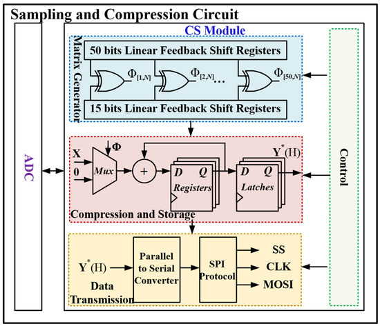
Figure 6.
The structure of the sampling and compression circuit.
4. Results and Discussion
4.1. Algorithm Simulation
The CS algorithm is simulated to evaluate the reconstruction performance of our circuit. The experimental data are obtained from the MIT-BIH database [20], and ten Records of men and women of different ages are selected for verification. The MIT-BIH database is chosen among the Internet–available ones as it is the most widely used in the scientific literature. The sampling frequency of the ECG signal in the database is 360 Hz, and a 10 kHz frequency is used to resample. The measurement matrix is binary, and the dimension M of the compressed data is 50. The reconstruction performance under various CFs is evaluated to improve the reliability of experimental results. The original data are 12 bits, where the low 4 bits are calculated approximately. The compressed data and the accurate accumulation sum of the high 8 bits are set to 24 and 16 bits, respectively, to prevent overflow.
Figure 7 reveals that the PRDs of ten ECG Records reconstructed data using two different calculation methods are less than 2%, indicating that the reconstruction performance is very good. The PRD of accurate calculation is slightly lower than that of approximate calculation. Although the approximate calculation sacrifices a little reconstruction quality, it is acceptable.
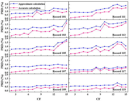
Figure 7.
The PRD of reconstruction signal of ten Records for two different calculation methods.
4.2. Circuit Simulation
The Monte-Carlo simulation is performed 1000 times for the offset voltage of the calibrated comparator of the SAR ADC. The results indicate that the offset voltage σ is 0.29 mV, and the average value of the offset voltage is −0.02 mV, as shown in Figure 8.
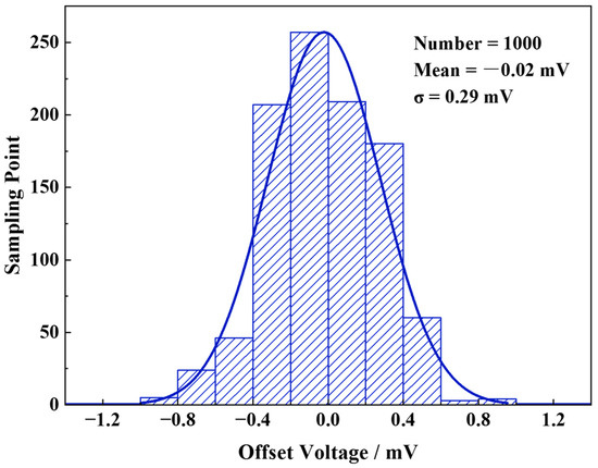
Figure 8.
The Monte-Carlo simulation of the calibrated comparator.
The PVT simulation is completed to evaluate the dynamic performance of the 12-bit SAR ADC at the sampling frequency of 10 kHz, and the simulation results are plotted in Figure 9. Under the condition of TT_1.2V_25 °C, the ENOB is 11.1 bits, SNR is 68.7 dB, and SFDR is 71.1 dB. The performance of ADC at TT_1.2V_25 °C is better than that of other processes, and at SS_1.08V_80 °C is the worst.
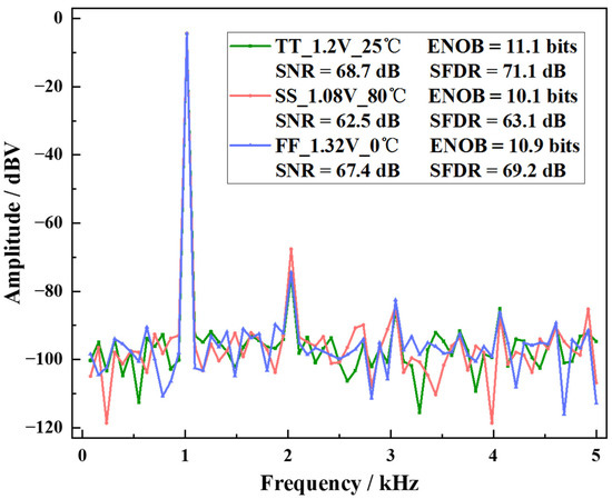
Figure 9.
The PVT simulation of the SAR ADC.
To evaluate the robustness of the SAR ADC against device mismatch, the Monte-Carlo simulation of the circuit is performed 100 times. The simulation results in Figure 10 show a mean of 9.85 bits with a standard deviation of 0.97 bits range.
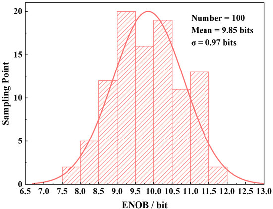
Figure 10.
The Monte-Carlo simulation of the SAR ADC.
Figure 11 presents the functional simulation of the sampling and compression circuit, where adc_to_cs is the 12-bit parallel ECG signal after ADC conversion, and cs_to_receiver is the compressed serial data of the high 8-bit ECG data. The system clock sys_clk is 100 kHz, and the sampling clock adc_sample_clk is 10 kHz. The CF is set to 8, so the dimension of the measurement matrix is 50 × 800, and 50 elements, namely prbs in Figure 11, are generated in each sampling clock cycle. The compressed data are transmitted according to the SPI protocol, and outputs include the enable signal ss_to_receiver, clock signal clk_to_receiver, and serial data cs_to_receiver. For every 8 bit of data transmission, each compression round requires 100 transfers.
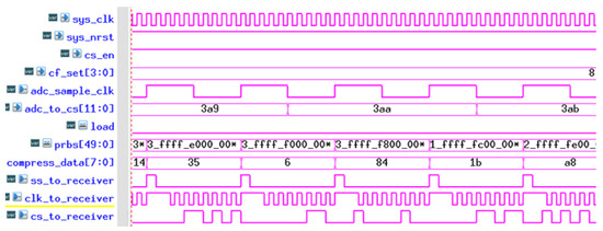
Figure 11.
The functional simulation of the sampling and compression circuit.
4.3. Circuit Implementation
In a 55 nm CMOS process, the physical layout of the proposed circuit is realized. The area of ADC is 0.011 mm2 (85 μm × 134 μm), and the power consumption is 0.214 μW at the sampling frequency of 10 kHz. The traditional CS module with accurate calculation and register storage has an area of 0.046 mm2 (215 μm × 214 μm) and a power consumption of 1.409 μW. In contrast, the optimized CS module based on approximate calculation and latch storage has an area of 0.037 mm2 (193 μm × 192 μm) and a power consumption of 0.963 μW. The area and power consumption of the proposed CS module are reduced by 19.5% and 31.7%, respectively, affording a remarkable optimization effect.
The sampling and compression circuit is designed based on the optimized ADC and CS module. As illustrated in Figure 12, the circuit area is 0.325 mm2 (570 μm × 570 μm), limited by IO, and the core area is 0.048 mm2 (220 μm × 220 μm).
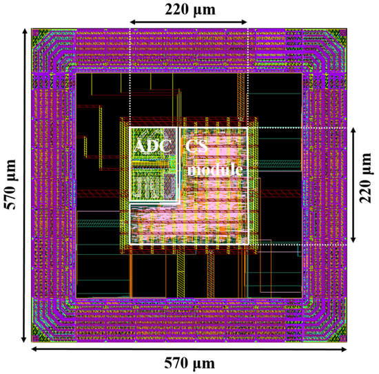
Figure 12.
The layout of the sampling and compression circuit.
The power consumption of the sampling and compression circuit is shown in Table 3. The total power consumption is 2.951 μW, where the IO power consumption is 1.612 μW, accounting for 54.6%, and the remaining 1.339 μW is the core power consumption.
Table 3.
The power consumption of the sampling and compression circuit.
We compare the proposed circuit against current solutions with the results reported in Table 4. A Figure of Merit (FOM) is used for fairness of the comparison under different processes, as shown in Equation (9):
Table 4.
The comparisons among different sampling and compression circuits.
References [10,11] only mention the hardware consumption of the CS module, while references [12,13] present the sampling and compression circuit results. Our work provides results for both the CS module and sampling and compression circuit, and Table 4 shows the hardware consumption of the sampling and compression circuit. Our 12-bit SAR ADC has a higher accuracy than the others, which is beneficial for data compression and reconstruction. References [10,11] adopt a relatively advanced low supply of 0.6 V compared with the 1.2 V used in this paper, but our CS module has obvious advantages with its area of 0.037 mm2 and power consumption of 0.963 μW. Compared with References [12,13], the proposed sampling and compression circuit has significant advantages in hardware consumption.
The accurate accumulation sum of the high part and the approximate accumulation sum of the low part are added to the remote server to obtain the compressed data for signal reconstruction. Figure 13 presents the results of reconstructing the compressed data. Since the reconstructed signal is almost identical to the original signal, we offset the original signal upward by 0.2 V for clarity. The measured PRD is 1.513%, which is consistent with the simulation results of the CS algorithm.
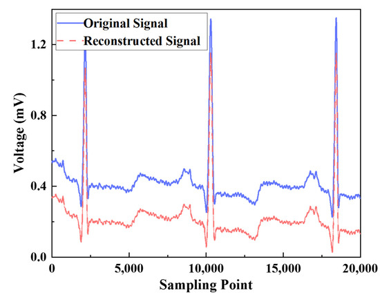
Figure 13.
The reconstruction results of the compressed data.
5. Conclusions
This paper proposes a novel ECG sampling and compression circuit to solve the problems of a large area and high power consumption. The 12-bit SAR ADC is customized and integrated into the sampling and compression circuit according to the data processing requirements. The capacitor array uses the top plate sampling scheme and bridge capacitors to reduce the area and power consumption, and the comparator applies a calibration technique to minimize the offset voltage to 0.29 mV. On the premise of ensuring the reconstruction quality, the CS module completes the matrix calculation, and pulsed latches store the results. The addition calculation approximates the addend, and accurate calculation and approximate calculation are carried out for the high and low parts of the ECG signal, respectively. The sampling and compression circuit realizes the functions of analog-to-digital conversion, matrix generator, compression and storage, and SPI output.
In a 55 nm CMOS process, the ADC area is 0.011 mm2, and the power consumption is 0.214 μW. The developed solution optimizes the CS module and reduces its area and power consumption by 19.5% and 31.7%, respectively. When the supply is 1.2 V and the frequency is 100 kHz, the area and power consumption of the sampling and compression circuit are 0.325 mm2 and 2.951 μW, respectively, presenting apparent advantages. The ECG signal reconstruction is completed based on the BSBL algorithm, with the measured PRD of the reconstructed data being less than 2%. Therefore, the proposed sampling and compression circuit has the advantages of low power consumption and high reconstruction performance, which can be used in medical monitoring and diagnosis.
Author Contributions
Conceptualization, Z.Z. and Z.Y.; methodology, Z.Z. and Y.N.; software, Z.Z. and X.C.; validation, Y.N. and X.C.; formal analysis, Y.N., X.X. and X.C.; investigation, Z.Z., Y.N. and X.X.; resources, Z.Y. and X.G.; data curation, Z.Z. and X.X.; writing—original draft preparation, Z.Z. and Z.Y.; writing—review and editing, Z.Z. and Z.Y.; visualization, Z.Z. and Z.Y.; supervision, Z.Y. and X.G.; project administration, Z.Y. and X.G.; funding acquisition, Z.Y. and X.G. All authors have read and agreed to the published version of the manuscript.
Funding
This research was funded by the Fundamental Research Funds for the Central Universities, grant number JUSRP51510, the Jiangsu Province Key Research and Development Program, grant number BE2019003-2, and the Joint Project of Yangtze River Delta Community of Sci-Tech Innovation, grant number 2022CSJGG0400.
Institutional Review Board Statement
Not applicable.
Informed Consent Statement
Not applicable.
Data Availability Statement
Data used in this paper can be found at https://www.physionet.org/physiobank/database/mitdb/ (accessed on 1 March 2023).
Conflicts of Interest
The authors declare no conflict of interest.
References
- Wei, P.C.; He, F.C. The Compressed Sensing of Wireless Sensor Networks Based on Internet of Things. IEEE Sens. J. 2021, 21, 25267–25273. [Google Scholar] [CrossRef]
- Wang, N.C.; Chen, Y.L.; Huang, Y.F.; Chen, C.M.; Lin, W.C.; Lee, C.Y. An Energy Aware Grid-Based Clustering Power Efficient Data Aggregation Protocol for Wireless Sensor Networks. Appl. Sci. 2022, 12, 9877. [Google Scholar] [CrossRef]
- Melek, M.; Khattab, A. ECG Compression Using Wavelet-Based Compressed Sensing with Prior Support Information. Biomed. Signal Process. Control. 2021, 68, 11. [Google Scholar] [CrossRef]
- Sun, T.J.; Ge, Q.D.; Wen, Y.B.; Guo, Y.F.; Li, M.D. An under-Sampling Array Signal Processing Method Based on Improved Hadamard Matrix. Appl. Sci. 2022, 12, 10769. [Google Scholar] [CrossRef]
- Unni, V.S.; Gavaskar, R.G.; Chaudhury, K.N. Compressive Sensing of ECG Signals Using Plug-and-Play Regularization. Signal Process. 2023, 202, 10. [Google Scholar] [CrossRef]
- Okabe, Y.; Kanemoto, D.; Maida, O.; Hirose, T. Compressed Sensing EEG Measurement Technique with Normally Distributed Sampling Series. IEICE Trans. Fundam. Electron. Commun. Comput. Sci. 2022, E105A, 1429–1433. [Google Scholar] [CrossRef]
- Saliga, J.; Kovac, O.; Andras, I. Analog-to-Information Conversion with Random Interval Integration. Sensors 2021, 21, 3543. [Google Scholar] [CrossRef] [PubMed]
- Sadasivuni, S.; Bhanushali, S.P.; Banerjee, I.; Sanyal, A. In-Sensor Neural Network for High Energy Efficiency Analog-to-Information Conversion. Sci. Rep. 2022, 12, 18253. [Google Scholar] [CrossRef] [PubMed]
- Qian, H.; Song, X.; Li, D.; Wang, Z. Generalized Analog-to-Information Converter with Analysis Sparse Prior. IEEE Trans. Circuits Syst. I. Regul. Pap. A Publ. IEEE Circuits Syst. Soc. 2021, 68, 3574–3586. [Google Scholar] [CrossRef]
- Chen, F.; Chandrakasan, A.P.; Stojanovic, V.M. Design and Analysis of a Hardware-Efficient Compressed Sensing Architecture for Data Compression in Wireless Sensors. IEEE J. Solid-State Circuits 2012, 47, 744–756. [Google Scholar] [CrossRef]
- Kumar, G.K.; Chatterjee, B.; Sen, S. CS-Audio: A 16 pJ/b 0.1-15 Mbps Compressive Sensing IC with DWT Sparsifier for Audio-AR. IEEE J. Solid-State Circuits 2022, 57, 2220–2235. [Google Scholar] [CrossRef]
- Pareschi, F.; Albertini, P.; Frattini, G.; Mangia, M.; Rovatti, R.; Setti, G. Hardware-Algorithms Co-Design and Implementation of an Analog-to-Information Converter for Biosignals Based on Compressed Sensing. IEEE Trans. Biomed. Circuits Syst. 2016, 10, 149–162. [Google Scholar] [CrossRef] [PubMed]
- Liu, X.; Richardson, A.G.; Van der Spiegel, J. An Energy-Efficient Compressed Sensing-Based Encryption Scheme for Wireless Neural Recording. IEEE J. Emerg. Sel. Top. Circuits Syst. 2021, 11, 405–414. [Google Scholar] [CrossRef]
- Djelouat, H.; Zhai, X.J.; Al Disi, M.; Amira, A.; Bensaali, F. System-on-Chip Solution for Patients Biometric: A Compressive Sensing-Based Approach. IEEE Sens. J. 2018, 18, 9629–9639. [Google Scholar] [CrossRef]
- Wang, X.; Chen, H.B. A Survey of Compressive Data Gathering in WSNs for IoTs. Wirel. Commun. Mob. Comput. 2022, 2022, 4490790. [Google Scholar] [CrossRef]
- Yu, Z.G.; Zhao, Z.Q.; Tian, Q.; Guo, J.; Huang, X.; Gu, X.F. An Improved Measurement Matrix Generator for Compressed Sensing of ECG Signals. Electronics 2022, 11, 3784. [Google Scholar] [CrossRef]
- Yang, Y.; Huang, F.; Fei, L.; Tang, Y. Design of an Adaptive ECG Signal Processing System Based on Compressed Sensing. In Proceedings of the 2020 5th International Conference on Universal Village (UV), Boston, MA, USA, 24–27 October 2020; pp. 1–5. [Google Scholar] [CrossRef]
- Liu, C.C.; Chang, S.J.; Huang, G.Y.; Lin, Y.Z. A 10-bit 50-MS/s SAR ADC with a Monotonic Capacitor Switching Procedure. IEEE J. Solid-State Circuits 2010, 45, 731–740. [Google Scholar] [CrossRef]
- Cheng, Y.L.; Tong, Y.F. Techniques for Offset Calibration in Comparators. In Proceedings of the International Conference on Electronic Information Engineering and Computer Science (EIECS), Changchun, China, 23–26 September 2021; pp. 838–847. [Google Scholar] [CrossRef]
- Picariello, F.; Iadarola, G.; Balestrieri, E.; Tudosa, I.; De Vito, L. A Novel Compressive Sampling Method for ECG Wearable Measurement Systems. Measurement 2021, 167, 108259. [Google Scholar] [CrossRef]


Disclaimer/Publisher’s Note: The statements, opinions and data contained in all publications are solely those of the individual author(s) and contributor(s) and not of MDPI and/or the editor(s). MDPI and/or the editor(s) disclaim responsibility for any injury to people or property resulting from any ideas, methods, instructions or products referred to in the content. |
© 2023 by the authors. Licensee MDPI, Basel, Switzerland. This article is an open access article distributed under the terms and conditions of the Creative Commons Attribution (CC BY) license (https://creativecommons.org/licenses/by/4.0/).