1. Introduction
In recent years, smart cities have been an evolving concept with many applications ranging from healthcare to Intelligent Transport systems (ITS) [
1,
2,
3,
4,
5,
6]. With the development of smart cities, the current challenges related to quick health access to remote patients, the reduction in traffic congestion, and smart industries can be achieved. This will lead to enhanced productivity and efficiency in various walks of life [
7,
8,
9,
10,
11,
12].
Blockchain is a digital concept to save data and maintains an immutable public record of transactions (ledger) without central authorities [
13,
14,
15]. Trust, security, program-ability, and maintenance are key advantages of Blockchain models. Decentralization, trust, security, sequential, and combine maintenance are offered by the Blockchain systems [
16,
17]. Due to the immutability and decentralized nature of Blockchain, it has the potential to revolutionize the increasing centralization of smart city applications [
18,
19,
20,
21,
22].
The Blockchain network generally consists of two nodes. The first is the normal nodes or users that generate Blockchain data. The second nodes are the full nodes that help in creating the data, enabling transactions between users, verifying the transactions, and maintaining a record of all user transactions. These full nodes have high computing capacity and handle requests for different data access and task completion from many normal user nodes [
23].
The database maintained by the full nodes generally utilizes the key–value store mechanism in which data are stored against a key–value pair. The key acts as an identifier for the value. The key–value databases have several advantages related to scalability and fast access to data. Hence, full nodes in Blockchain utilize this data access mechanism in their cache.
Field-Programmable Gate Array (FPGA) technology is useful to implement hardware caching techniques due to its low computational power, good flexibility, and high parallelism. FPGA can process several off-chain transactions out of Blockchain, which increases the throughput and obtains the required latency. Moreover, FPGA can also implement protocols used in the Blockchain process such as hashes, digital signatures, and encryption that need large computational power [
24].
For Blockchain, an FPGA-based multiple-step cached system can be developed by using Dynamic Random-Access Memory (DRAM) and Block Random-Access Memory (BRAM), which accelerates the processing speed of Blockchain [
25,
26,
27,
28]. A major challenge is to implement hardware caching techniques that improve the speed of data access by increasing the hit rate of the cache and reducing the miss rate. The hit rate in our proposed work refers to the chance of accessing data from the cache instead of the main memory for the Blockchain key–value store application. It should be noted that if the cache hit rate is increased, the data access can be quick as it takes a significantly longer time to search and retrieve results from the main memory.
In this paper, we implement different caching techniques such as direct mapping, 2-way set-associative mapping, and 4-way set-associative mapping for key–value store-based Blockchain applications on an FPGA. The work presents a detail of cache implementation including the flow diagram and Finite State Machine (FSM). The performance of the mapping techniques is analyzed for different key sizes. Results highlight that the cache hit and cache miss ratio of the 2-way and 4-way associative technique is much better than the direct-mapping technique.
2. Related Work
2.1. Literature Review
FPGA is useful in implementing the hardware caching systems as well as many other Blockchain processes such as evaluating the time for digital signature, hash evaluation, etc. In [
19], the process of a novel key management scheme for key transfer among security managers in heterogeneous networks is proposed. The Blockchain structure allows secure key transfer within the decentralized network, which decreases the Blockchain key transfer time.
As the digital signature algorithm is needed for all transactions in the Blockchain, the work in [
18] developed a model on FPGA NIC, which has a key–value data store system written in a P4 language. Commands (issue, transfer, refer, and create) are used for transferring digital assets in this prototype system. The result of the prototype systems concerning throughput and latency is compared with other Blockchain software applications in which the latency is 15.4 times lower and the throughput 6.04 times higher. The FPGA-based system enhanced the system performance by reducing the processing time.
The work in [
24] addressed the FPGA implementation of the Elliptic Curve Digital Signature Algorithm (ECDSA), which is acceptable for cryptocurrencies in Blockchain. The simulation result shows the superiority of FPGA implementation over software-based computation using a Central Processing Unit (CPU). Blockchain is a key technology of cryptocurrency that supports a distributed ledger without an administrator. The amount of Blockchain data is increased because all transactions need to be stored to enable the Blockchain. To respond quickly to Simplified Payment Verification (SPV) nodes for verification of the transaction, the author designed the key–value store (KVS) hardware cache on FPGA NIC [
20]. The SPV node accesses the Blockchain via the full node for verification of the transaction because the SPV node does not contain all the transaction records. Throughput is calculated by counting the number of requests processed by the Blockchain server, which shows that it has been improved from 6.3 to 7.45 times when the cache is hit.
In [
21], the authors designed a modified Secure Hashing Algorithm (SHA)-256 hash core that improves hashing execution to achieve efficient Blockchain caching. The author also investigated the bottleneck performance system in Blockchain applications and presented an efficient FPGA caching system that enhanced the scalability and throughput of Blockchain.
In [
22], the authors designed a hardware cache system that enhanced the read performance of the Blockchain application without changing the protocol. This decreased power consumption because software applications on a server utilize more energy than the proposed systems on the FPGA NIC and increase the throughput of the system. In the peer-to-peer network of Blockchain, the full node verified whole transactions in the network. Some Blockchain users such as personal mobile users do not act as full nodes because the workload of the full node is quite high for them [
20]. When many users try to access the full node for queries, such as transaction contents, balance confirmations, and histories of transactions, searching the throughput of the full node becomes the bottleneck of the Blockchain system. To overcome this drawback, different techniques and hardware (GPU, FPGA, etc.) are used to accelerate the throughput of Blockchain searching.
Different from the previous work on hardware caching techniques for Blockchain applications, we have implemented the 2-way and 4-way set-associative techniques and evaluated the performance gain. Previously, in the literature, the work in [
18] implemented direct-mapped cache for Blockchain applications. To the best of our knowledge, 2-way and 4-way set-associative techniques have not been used for the key–value store-based Blockchain applications.
Table 1 gives a comparison between CPU, GPU, and FPGA in terms of hash rate and efficiency rating. The hash rate is the speed of mining [
29]. The hash rate is a measure of the computational power needed per second to process transactions and mine new coins. The Blockchain or digital ledger is added to each transaction in the cryptocurrency network. According to
Table 1, the mining rate of FPGAs is 2533 Mhash/second and the efficiency rating is 0.709 hash/second/dollar. The reasoning behind the low-efficiency rating for FPGA is that FPGA mining is still relatively new.
Table 2 discusses a summary of recent state-of-the-art Blockchain implementations to accelerate searching in Blockchain.
2.2. Overview of the Caching System on FPGA NIC for Blockchain
The conventional key–value stores (KVS) hardware cache system is shown in
Figure 1. The dashed arrows indicate the cache miss behavior whereas the bold arrow indicates the cache hit behavior. The cache system is designed on Reduced Latency Dynamic Random-Access Memory (RLDRAM) and is based on a direct-mapped method to mitigate cache complexity [
22].
Figure 1.
Hardware cache system for a cache hit and cache miss.
Figure 1.
Hardware cache system for a cache hit and cache miss.
Table 2.
Summary of recent state-of-the-art Blockchain implementations to accelerate Blockchain.
Table 2.
Summary of recent state-of-the-art Blockchain implementations to accelerate Blockchain.
| Key Idea | Results Obtained |
|---|
| Throughput improvement of Blockchain operations [18] | Throughput improved by 6.04 times
Latency reduced by 15.4 times |
| FPGA NIC for Caching in Blockchain [20] | FPGA NIC of 10 GB used
FPGA cache hits improvement by 13% |
| FPGA-based caching for Blockchain [28] | Improved scalability
Improved throughput
Reduced area utilization
Reduced power consumption |
| FPGA-based caching for Blockchain [20] | Throughput improved by 1.97 times
Decreased power consumption by 18.5 W |
| Improved Blockchain full node search using GPUs [30] | Higher throughput than CPU-based search
Higher throughput than other GPU-based searches |
At first, the client requests the host to obtain data as shown in
Figure 1. The DRAM controller receives the request and extracts the key. It first searches the key on DRAM; if the data are present in the DRAM, it will be a cache hit and FPGA NIC will reply with the result to the client. If the data are not present in DRAM, then it will be a cache miss. The DRAM controller forwards the request from the client to the server in case of a cache miss. The server checks for the key, replies to the client, and sends the result to FPG NIC. The RLDRAM in FPGA NIC saves the data sent by the server for the future.
3. Implemented Caching System
Cache memory is more expensive but it is faster than the main memory. This paper explored three different caching systems for Blockchain applications and implemented them on the FPGA NIC. These include the traditionally used direct-mapped cache, 2-way set-associative cache, and 4-way set-associative cache. The set-associative cache system increases the cache complexity compared with the direct-mapped caching; however, it reduces the conflict miss and increases throughput.
Table 3 shows a summary of proposed cache characteristics.
In this paper, we implemented direct-mapped, 2-way, and 4-way set-associative cache techniques on BRAM and examined their performance by calculating the cache misses versus cache hits. The capacity of BRAM is 11,664 Kb. The memory capacity of BRAM is less than that of RLDRAM; however, the processing speed of BRAM is faster than that of RLDRAM. Therefore, BRAM can accelerate work further as an intermediate cache system. BRAM will act as a first-level cache and RLDRAM will act as a second-level cache in Blockchain systems. The controller will search first in the level one cache: if it hits, it will reply; otherwise, it will go to the next level. The frequently used data will save in the level one cache.
Figure 2 shows the hardware implementation of the implemented caching system on FPGA NIC for Blockchain. FPGA NIC has three states to manage the KVS system. These include packet forwarding, access onboard BRAM, and key extraction.
Key extraction: The User Datagram Protocol (UDP) packets have requested addresses with pre-specified destination port numbers. From these requesting packets, the FPGA NIC extracts the payload.
Figure 3 shows the format of requesting packets. The requesting packet consists of a header and payload. The requesting packet’s length is 74 bytes with which the length of the header is 42 bytes and the length of Transaction ID (TXID) is 32 bytes. The Advanced Extensible Interface (AXI) bus width is 32 bytes; so, FPGA needs 3 cycles to extract the payload from a 74-byte packet.
Access Onboard DRAM: The single cache line is 512 bits and includes “Tag”, “Index”, and “Value”. The value is 256 bits Merkle Root, whereas the lower 12 bits of the payload are “Index” and the upper 244 bits of payload are “Tag”. Valid registers are used corresponding to every index, which shows valid flags to check whether the cache hit or missed.
The BRAM controller accesses onboard BRAM upon receiving a requesting packet and finds if it is a hit or a miss. When the server saves data in the cache line, it enables the valid flag. The BRAM controller judges cache hits when the tag value saved in the cache is equal to the 244-bit value generated from the requesting packet. On the other hand, it judges a cache miss. When the FPGA NIC is processing data, the accessing onboard DRAM must stop receiving new packets because the processing speed of the FPGA is less than its access latency. For result evaluation, we use one delay cycle to obtain data from the BRAM cache and three delay cycles to obtain data from the server (main memory).
Figure 4 shows the basic layout of the proposed caching system.
Figure 3.
Requesting packet format.
Figure 3.
Requesting packet format.
Figure 4.
Layout of caching system.
Figure 4.
Layout of caching system.
Packet Forwarding: The FPGA NIC forwards the requesting packet to the server when the cache misses. Upon cache hits, the FPGA NIC creates a new UDP packet whose payload changes to Merkle root by modifying the requesting packet. The TXID, source IP, and MAC address of the requesting packet must modify the packets before forwarding them to the client. The TXID changes to Merkle root in the payload and the source IP and MAC addresses change with destination IP and MAC addresses. The length of replying packets remain equal to that of the requesting packet, which is 74 bytes.
Finite State Machine of Cache Read and Write Request
Figure 5 shows the Finite-state machine (FSM) of the cache system. There are eight states in the FSM of the cache system, as described below.
IDLE: The initial state of the cache controller. When it is reset, all the controlling output and input will be zero to the cache controller. All the operations are stopped in this state.
Request from CPU: In this state, the cache controller will check the request from the processor to access the memory and find if it is a written request or a read request. Depending upon the request, the controller will jump to the desired state.
Cache read: The cache controller jumps to this state on the cache read request. The cache controller checks whether it is a hit or a miss. The data will be provided to the processor when the cache is hit. Otherwise, the cache has no data, so it jumps to the next state.
Main Memory read: On cache miss case, the cache controller will jump to this state. The cache controller reads data from the main memory.
Bring Data to Cache: After reading data from the main memory, the controller jumps to this state. The controller writes data to the available location in cache memory. After writing data in the cache, the cache controller will jump to the next state.
Output data: The cache controller will provide data from the cache memory to the processor and jumps to first the state, i.e., request from CPU.
Figure 5.
FSM of cache system for read and write request.
Figure 5.
FSM of cache system for read and write request.
Figure 6 shows the flow chart diagram of the cache system. The flow chart diagram shows the detailed working of both the read and the write processes in the proposed system. When there is a write request, the first check is in the cache. If the data are present in the cache, they will not be stored again in the main memory. However, if the data are not present in the cache, it will store data in the main memory and then jump to a request from the CPU to wait for the next incoming request. When it is a read request, it first checks the cache. If the data are present in the cache, it provides output to the processor and waits for a new request from the CPU. On the other hand, if the data are not present in the cache, it fetches data from the main memory to the cache and provides output to the CPU.
4. FPGA Implementation Details of Cache Mapping
Mapping is a technique or process that focuses on how the data from the main memory is brought to the cache memory. In other words, mapping explains how data are duplicated or mapped (from main memory to cache memory) when there is a cache miss. As discussed in the last section, we used three cache mapping techniques: (1) direct-mapping technique; (2) 2-way set-associative mapping technique; (3) 4-way set-associative mapping technique. These three techniques are briefly discussed below.
4.1. Direct Mapping
A direct-mapped cache is the simplest cache system in which each main memory address can map to exactly one cache block. A direct-mapped cache can mitigate cache complexity. We use
to find which cache block can map to the main memory address, where
K is the block number of main memory and
N is the number of sets in the cache. For example, if there is a four-block cache, the main memory block number 10 goes to cache line 2 (10 mod 4 = 2). The block diagram of the implemented direct-mapped cache is shown in
Figure 7.
Figure 7 shows that when a valid flag is high and the tag saved in the cache block is equal to the 244-bit tag extracted from the request packet, then it will be cache hit and gets data out. On the other hand, if there is a cache miss, the BRAM controller forwards the request packet to the server. The server checks for the key, replies to the client, and also sends the result to the cache, as shown in
Figure 2.
Figure 8 shows the FSM of the direct-mapped cache system for the cache hit or miss case.
The various states are described in more detail below.
IDLE: In this state, the incoming cache requests are received and placed in the input registers.
Valid check and Tag compare: On read request, the cache controller jumps to this state and makes the busy signal of the system high. It checks the tag and makes state transitions based on hit or miss and validity.
Evict process: If validity is high and the tag comparison miss, then the evicting process starts. In this state, it evicts data in the required cache line, sends them to the main memory, and prepares the required cache line for a refill.
Evict wait: In this state, it waits until the evict process ends.
Refill data request: After tag comparison, if it is not valid or valid and miss but the evict process ends and the delay counter is zero, then the cache controller requests for data refill in the desired cache line.
Wait refill: In this state, it will wait until the refill process ends.
Data write: In this state, the data fetched through the refill process from the main memory is written in the desired cache line.
Data read: After the tag comparison, if it is valid and hit, it will read data directly from the cache.
Output data: It provides data to the processor after data is written in the cache and read from the cache. After that, the cache controller makes the busy signal low and jumps to the IDLE state.
The FSM of the direct-mapped cache controller unit differs from the basic FSM cache discussed above due to the evict process, waiting for eviction response, and various latency interfaces. The FSM cache controller used in this research has a hit latency of one cycle and a miss latency of three cycles to respond to the request.
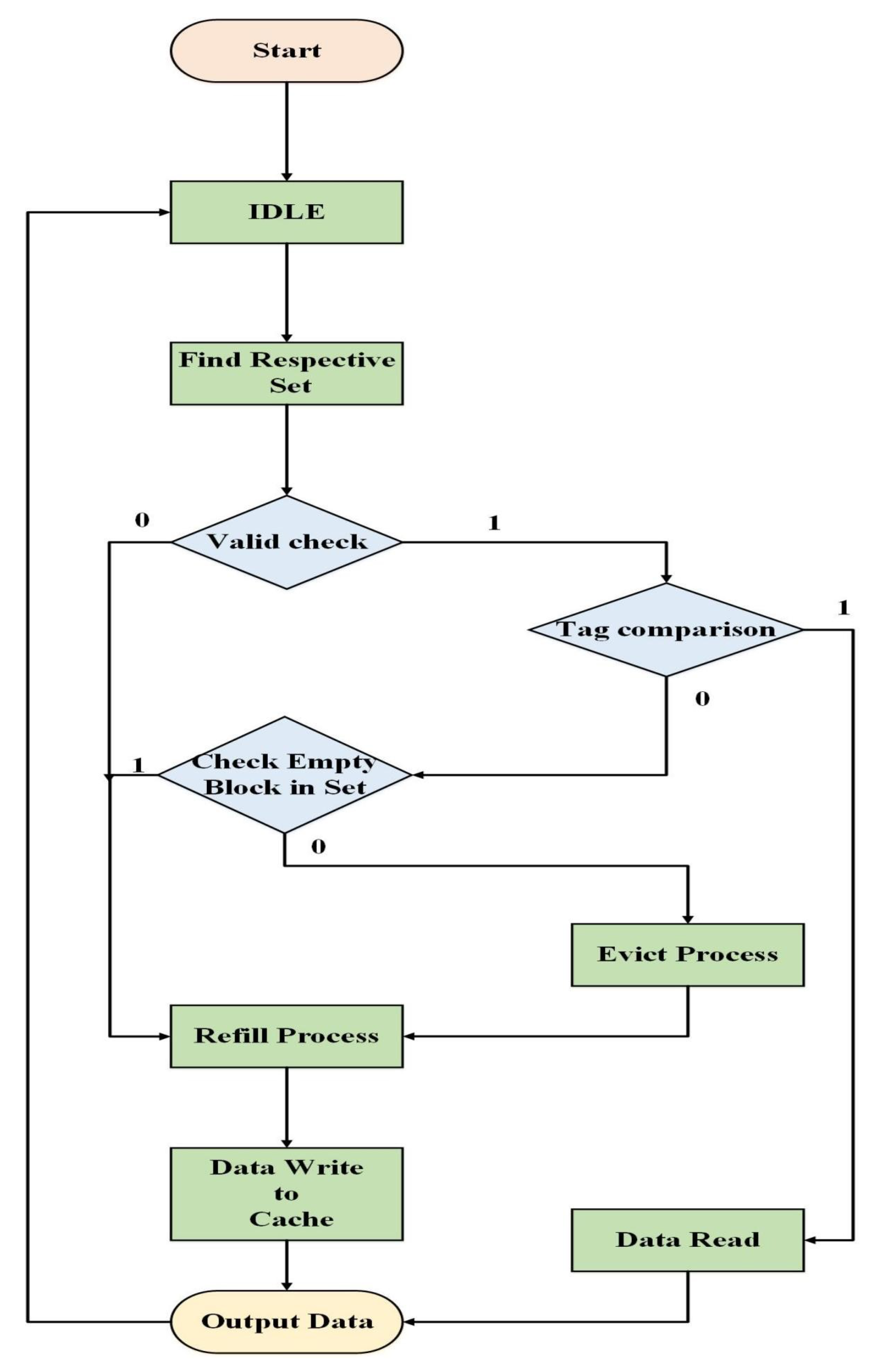
Figure 9 shows the flow chart diagram of the direct-mapped cache system. In direct mapping, when the controller receives the request, it checks the valid register. Based on the valid check result, it decides to go to the tag comparison or refill process. If the valid register is high, it goes to the tag comparison; if the valid register is low, it directly goes to the refill process. After tag comparison, it goes to the evict process if the tag does not match or there is a cache miss. On the other hand, if data are present in the cache, then the cache controller reads data from the cache and sends the output to the processor.
4.2. 2-Way Set-Associative Mapping
N-way set-associative cache provides N blocks in each set to decrease conflict, where N is the cache’s degree of associativity. For each memory address, the data can map to any block in the set. The set of the memory address can be found using . In our implemented work, we designed a 2-way set-associative cache and a 4-way set-associative cache on BRAM.
Figure 10 shows the cache layout of the 2-way set-associative cache system. According to the NetFPGA-10G team, the total capacity of BRAM is 11,664 Kbits. The memory capacity of BRAM is less than RLDRAM. However, the processing speed of BRAM is faster than that of RLDRAM. Therefore, BRAM can accelerate work further as an alternate cache. In
Figure 10, the
value/data are shown in green, and
Tag is shown in red. A single set of 2-way set-associative caches contains two blocks of data using up to 1024 bits. From the accessible memory of BRAM, we create 6000 sets for a 2-way set-associative cache system.
For example, when two memory addresses map to set 4, the 2-way cache system can accommodate data from both addresses, as shown in
Figure 11. The cache miss will happen during the first loop iteration and both words are loaded into the two ways of set 4. For the next iterations of these addresses, the cache will hit. If these addresses repeat 5 times each, then the miss rate is 2/10 = 20%; however, the miss rate will be 100% for the direct-mapped cache because the data change in a particular cache line for every repetition of addresses. In a set-associative cache system when both ways are full, the question will arise of which way to replace. In our work, we use the Least Recently Used (LRU) algorithm for the replacement of the ways [
29].
4.3. 4-Way Set-Associative Mapping
In this work, we design a 4-way set-associative cache system by using the LRU algorithm method.
Figure 12 shows the cache layout of the 4-way set-associative cache system. Each set of 4-way set-associative cache contains 4 blocks of data. To test the 4-way cache system design, we create
sets, as shown in
Figure 12.
Tag is shown in red color and
Value is shown in green color. A single set of 4-way cache systems containing
Tag and
Value uses up to 2048 bits of memory. 4-way set-associative cache has fewer data conflicts, so it has lower miss rates than direct mapping and 2-way cache mapping. The LRU replacement algorithm is used to replace memory blocks when it needs to replace an already occupied memory block [
29].
4.4. FSM and Flow of Set-Associative Technique
Figure 13 shows the FSM of the set-associative cache mapping system. Different states of FSM are described below:
IDLE: This state receives the incoming cache request and places them in the input registers. The cache controller jumps to the next state if it reads the request signal and makes the busy signal high. During the high busy signal, the cache controller will not receive any new data.
Set number and valid check: In this state, the cache controller jumps to the respective set and checks the valid register. If the valid register is zero, the cache controller jumps to the refill process, and if the valid register is one, the cache controller jumps to the next state for cache comparison.
Tag compare: When the valid register is one, the cache controller jumps to this state and starts tag comparison. If the tag of the incoming address matches with the tag of a respective block of the set, the controller jumps to the next state, i.e., data read state. On the other hand, if it misses, the cache controller jumps to another state, i.e., checks an empty block in the set.
Data read: After the tag comparison, if it is valid and hit, it will read data directly from the cache.
Check empty block in set: Based on the 2-way and 4-way cache system, the cache controller checks for an empty block in the set. If there is an empty block in the set, the cache controller jumps to the refill process to request write data in an empty block of the set. On the other hand, the cache controller decides which block of the set will go for the evict process based on the Least Recently Used (LRU) algorithm and jumps to the next state, i.e., the evict process.
Evict process: In this state, it evicts data in the required cache block of the set, sends it to the main memory, and prepares the required cache block of the set for the refill process.
Evict wait: In this state, it waits until the evict process ends.
Refill data request: If there is an empty block in the set and the delay counter is zero, the cache controller jumps to this state and searches respective data in the main memory to refill the cache block.
Wait refill: In this state, it will wait until the refill process ends.
Data write: The cache controller writes the data fetched through the refill process from the main memory to the desired cache line.
Output data: It provides data to the processor after data write in the cache and read from the cache. After that, the cache controller makes the busy signal low and jumps to the IDLE state for a new request.
This FSM is used for both 2-way and 4-way cache systems. The difference between a 2-way and 4-way cache system is the number of blocks in the set. In a 2-way cache system, there are two blocks in the set, and a 4-way cache block has four blocks in the set. The FSM of the cache controller of set-associative is different from the direct-mapped controller FSM. In this controller, after tag comparison, if there is a miss, it goes to check any other empty block in the set rather than going for the evict process. This saves the three-cycle cache miss penalty.
Figure 13.
FSM of set-associative cache technique.
Figure 13.
FSM of set-associative cache technique.
Figure 14 shows the flow chart diagram for the cache controller of both 2-way cache mapping and 4-way cache mapping techniques. After obtaining the read address from the CPU, it goes to the respective set and checks the valid register. If the valid register is one, the cache controller goes for tag comparison; otherwise, it requests the refill process. If the valid register is one and the tag does not match, the cache controller checks for an empty block in the set. If there is an empty block, the data are stored in that empty block of the set, and if all blocks in the sets have data, it searches the least recently used block in the set according to the LRU algorithm and sends the least recently used block for the evict process.
5. Results and Discussion
This section discusses the simulation results of direct cache mapping, 2-way set-associative cache mapping, and 4-way set-associative cache mapping after the post and route synthesis report. Verilog HDL is used and the Zynq-7000 FPGA evaluation board is used for cache technique implementation. Results compare 2-way and 4-way set-associative with a direct-mapped cache by simulation with respect to the hit rate and the miss rate. A 64-byte input address is generated from the Bitcoind core software used to compare different cache organizations. Bitcoind [
31] implements the Bitcoin protocol for Remote Procedure Call (RPC) use. From these addresses, we create four sets of addresses and data for performance comparison of cache systems. We use 10 K, 25 K, and 50 K key address sets to analyze the system.
5.1. Delay When a Cache Hit or Miss Occurs
The operating frequency for each cache system is fixed as 200 MHz for fair comparison between them. The average access time is also the same for direct-mapped and set-associative cache techniques in the proposed system at the cost of extra resources used in the set-associative cache technique. In the 2-way and 4-way set-associative techniques, the average access time is not increased as the memory indexing depth is the same in all proposed cache systems. The average access time is = 5 ns when the cache hits. On the other hand, if the cache is missed, the additional main memory access time will be added, which in this case is equal to 30 ns (i.e., 6 clock cycles). In addition, in the 4-way set-associative cache, the miss rate is lower than the other techniques; so, the chance to access main memory is lower than the other techniques. Eventually, this significantly improves the average access time as the main memory access time can be significantly greater than the cache access time for a large number of keys.
Figure 15 shows that the cache controller takes one clock cycle to obtain output when a cache is hit, whereas it takes three cycles of a clock to obtain output when a cache is missed. In
Figure 15, the first two inputs are the cache miss case and it takes three cycles to obtain output, whereas the other two input addresses are of the cache hit case. Therefore, after one cycle, we instantly obtain the output data. The wait signal shows if we are accessing the memory or not. When the wait signal is zero, it means that the memory is being accessed and there will be no new input data. The wait signal is zero when there is a cache hit. The signal
hit shows if it is a cache hit or miss. There is always a cache miss when the data are being read for the first time; so, the cache controller receives output from the server and data are saved in the cache. In the subsequent access request for the same data, we receive output from the cache and the hit becomes one.
5.2. Comparison of Cache Hit Rate and Miss Rate
Table 4 shows cache hit and cache miss in the direct-mapped cache system, 2-way cache system, and 4-way cache system for 10 K key addresses. The cache hit rate and cache miss rate are calculated by counting the clock cycle for a cache hit and miss. Equations (
1) and (
2) calculate the cache hit ratio and cache miss ratio, respectively.
Table 4 shows that the cache hit ratio in 2-way and 4-way is greater than that of the direct-mapped cache system, whereas the cache miss ratio in direct mapping is greater than the 2-way and 4-way set-associative cache system. It can be seen that the gap between a cache hit and cache miss is very small in this result. This is because of the small set of keys used for comparison. However, this gap will increase as we use large sets of keys for comparison, as shown in
Table 5,
Table 6 and
Table 7.
Table 5 shows the cache hit ratio and cache miss ratio comparison for 25 K key addresses. The hit ratios of 2-way and 4-way cache systems are 77.09% and 78.33%, whereas the hit ratio of direct-mapped cache systems is 76.32%. The cache miss ratio of the direct-mapped cache system is 23.67% and the cache miss ratios of 2-way and 4-way cache systems are 22.9% and 21.67%, respectively. The differences between the cache hit ratio and cache miss ratio of the direct-mapped and 2-way cache system are 0.77% and 0.78%, and the differences between the cache hit ratio and cache miss ratio of the direct-mapped and 4-way cache system are 2.01% and 2%.
Table 6 shows the cache hit ratio and cache miss ratio comparison for 50 K key addresses. The hit ratios of 2-way and 4-way cache systems are 75.27% and 76%, while the hit ratio of the direct-mapped cache system is 73.6%. The cache miss ratio of the direct-mapped cache system is 26.4% and the cache miss ratio of the 2-way and 4-way cache system is 24.73% and 24%, respectively. The difference between the hit ratio of the direct-mapped and 4-way cache system is 2.4% and the difference between the hit ratio of the direct-mapped and 2-way cache system is 1.67%.
Table 7 shows the cache hit rate improved by set-associative techniques with respect to the direct-mapped cache technique. The hit rate improved by the 2-way set-associative technique with respect to the direct-mapped cache technique for 10 k, 25 k, and 50 k keys sets are 0.8%, 0.77%, and 1.67%, respectively; whereas, for these sets of keys (i.e., 10 k, 25 k, and 50 k), the hit rate improvement of the 4-way set-associative technique with respect to the direct-mapping technique is 0.92%, 2.01%, and 2.4%, respectively.
Table 7 also shows that the hit rate is improved by set-associative techniques. This shows that the set-associative technique can perform better compared to direct mapping for a large set of keys.
The results related to resource utilization of three cache techniques are given in
Table 8. Results show that the set-associative technique utilizes more resources in terms of RAM, Look-up Tables (LUTs), and slice registers compared to the direct-mapped caching. For example, the 4-way set-associative technique requires nearly four times the RAM and twice the number of LUTs and registers compared to the direct-mapped technique. The additional cost of using higher resources provides advantages in terms of improved cache hit rates and access time.
5.3. Discussion
As per the results, it is evident that for the given application, the direct-mapped cache provides around a % lower hit ratio but has the advantage of utilizing less resources, i.e., RAM and Slice LUTs. On the other hand, set-associative techniques have a better hit ratio achieved at the cost of a higher number of resources.
Both of these cache techniques can be useful for different Blockchain applications. In many Blockchain scenarios, common key–value pairs exist in the database that represent frequently used transactions [
23]. For these applications, a small increase in hit ratio will also significantly improve the overall access delay, as common key–value pairs will be accessed using the cache. Thus, the effective hit ratio will be more than the actual hit ratio in these cases. For other Blockchain applications, where such common key–value pairs do not exist and where the speed of data access is less critical, the direct-mapped cache could be a cost effective caching technique.
6. Conclusions
Efficient use of caching for quick data access is a major challenge in Blockchain. In particular, for a key–value database used in Blockchain, the caching system can improve the number of transactions handled by the full nodes. In this paper, we implement different caching schemes on FPGA NIC and analyze their performance in terms of metrics such as cache hit rate and cache miss rate. We designed 2-way and 4-way cache techniques on BRAM and compared them with the direct-mapped cache technique. Although set-associative cache systems increase cache complexity, they improve the cache hit ratio. The improvement in the hit ratio of the 2-way set-associative cache technique with respect to the direct-mapped cache technique for 10 K, 25 K, and 50 K keys are 0.8%, 0.77%, and 1.67%, respectively. Meanwhile, the same sets of keys, the hit rate improved by the 4-way set-associative cache technique with respect to the direct-mapping cache technique is 0.92%, 2.01%, and 2.4% respectively. The improvements in hit rate for large data sets show that 2-way and 4-way set-associative cache techniques perform better than direct-mapped cache techniques for caching systems. In the future, when a multilevel cache system is used Blockchain, BRAM can act as a level one cache and RLDRAM can act as a second-level cache to accelerate the caching delay. Moreover, we will investigate the use of multiple FPGAs in parallel for accelerating the Blockchain mining operation.
Author Contributions
This article was prepared through the collective efforts of all the authors. Conceptualization, M.F.S., F.A., M.A.J., M.B.K., A.K.J.S., M.A. and M.H.A.H.; writing—original draft, M.F.S., F.A. and M.A.J.; writing—review and editing, M.B.K., A.K.J.S. and M.A. All authors have read and agreed to the published version of the manuscript.
Funding
The authors extend their appreciation to the Deanship of Scientific Research at Imam Mohammad Ibn Saud Islamic University for funding this work through Research Group no. RG-21-07-07.
Institutional Review Board Statement
Not applicable.
Informed Consent Statement
Not applicable.
Data Availability Statement
Not applicable.
Conflicts of Interest
The authors declare no conflict of interest.
References
- Giordani, M.; Polese, M.; Mezzavilla, M.; Rangan, S.; Zorzi, M. Toward 6G Networks: Use Cases and Technologies. IEEE Commun. Mag. 2020, 58, 55–61. [Google Scholar] [CrossRef]
- Na, Z.; Liu, Y.; Shi, J.; Liu, C.; Gao, Z. UAV-supported Clustered NOMA for 6G-enabled Internet of Things: Trajectory Planning and Resource Allocation. IEEE Internet Things J. 2020, 8, 15041–15048. [Google Scholar] [CrossRef]
- Javed, M.A.; Zeadally, S.; Hamida, E.B. Data analytics for Cooperative Intelligent Transport Systems. Veh. Commun. 2019, 15, 63–72. [Google Scholar] [CrossRef]
- Zhang, S.; Liu, J.; Guo, H.; Qi, M.; Kato, N. Envisioning Device-to-Device Communications in 6G. IEEE Netw. 2020, 34, 86–91. [Google Scholar] [CrossRef] [Green Version]
- Saad, W.; Bennis, M.; Chen, M. A Vision of 6G Wireless Systems: Applications, Trends, Technologies, and Open Research Problems. IEEE Netw. 2020, 34, 134–142. [Google Scholar] [CrossRef] [Green Version]
- Malik, U.M.; Javed, M.A.; Zeadally, S.; Islam, S.u. Energy-Efficient Fog Computing for 6G-Enabled Massive IoT: Recent Trends and Future Opportunities. IEEE Internet Things J. 2022, 9, 14572–14594. [Google Scholar] [CrossRef]
- Mao, B.; Kawamoto, Y.; Kato, N. AI-Based Joint Optimization of QoS and Security for 6G Energy Harvesting Internet of Things. IEEE Internet Things J. 2020, 7, 7032–7042. [Google Scholar] [CrossRef]
- Javed, M.A.; Nguyen, T.N.; Mirza, J.; Ahmed, J.; Ali, B. Reliable Communications for Cybertwin driven 6G IoVs using Intelligent Reflecting Surfaces. IEEE Trans. Ind. Inform. 2022, 18, 7454–7462. [Google Scholar] [CrossRef]
- Zeadally, S.; Javed, M.A.; Hamida, E.B. Vehicular Communications for ITS: Standardization and Challenges. IEEE Commun. Stand. Mag. 2020, 4, 11–17. [Google Scholar] [CrossRef]
- Malik, U.M.; Javed, M.A. Ambient Intelligence assisted fog computing for industrial IoT applications. Comput. Commun. 2022, 196, 117–128. [Google Scholar] [CrossRef]
- Malik, U.M.; Javed, M.A.; Frnda, J.; Rozhon, J.; Khan, W.U. Efficient Matching-Based Parallel Task Offloading in IoT Networks. Sensors 2022, 22, 6906. [Google Scholar] [CrossRef] [PubMed]
- Ahmed, J.; Nguyen, T.N.; Ali, B.; Javed, A.; Mirza, J. On the Physical Layer Security of Federated Learning based IoMT Networks. IEEE J. Biomed. Health Inform. 2022, 27, 691–697. [Google Scholar] [CrossRef] [PubMed]
- Nguyen, D.; Ding, M.; Pathirana, P.; Seneviratne, A.; Li, J.; Poor, V. Cooperative Task Offloading and Block Mining in Blockchain-based Edge Computing with Multi-agent Deep Reinforcement Learning. IEEE Trans. Mob. Comput. 2021, 22, 2021–2037. [Google Scholar] [CrossRef]
- Guo, S.; Dai, Y.; Guo, S.; Qiu, X.; Qi, F. Blockchain Meets Edge Computing: Stackelberg Game and Double Auction Based Task Offloading for Mobile Blockchain. IEEE Trans. Veh. Technol. 2020, 69, 5549–5561. [Google Scholar] [CrossRef]
- Jameel, F.; Javed, M.A.; Zeadally, S.; Jäntti, R. Efficient Mining Cluster Selection for Blockchain-Based Cellular V2X Communications. IEEE Trans. Intell. Transp. Syst. 2021, 22, 4064–4072. [Google Scholar] [CrossRef]
- Nguyen, D.C.; Pathirana, P.N.; Ding, M.; Seneviratne, A. Privacy-Preserved Task Offloading in Mobile Blockchain with Deep Reinforcement Learning. IEEE Trans. Netw. Serv. Manag. 2020, 17, 2536–2549. [Google Scholar] [CrossRef]
- Zhang, K.; Cao, J.; Leng, S.; Shao, C.; Zhang, Y. Mining Task Offloading in Mobile Edge Computing Empowered Blockchain. In Proceedings of the 2019 IEEE International Conference on Smart Internet of Things (SmartIoT), Tianjin, China, 9–11 August 2019; pp. 234–239. [Google Scholar] [CrossRef]
- Sakakibara, Y.; Tokusashi, Y.; Morishima, S.; Matsutani, H. Accelerating Blockchain Transfer System Using FPGA-Based NIC. In Proceedings of the 2018 IEEE Intl Conf on Parallel & Distributed Processing with Applications, Ubiquitous Computing & Communications, Big Data & Cloud Computing, Social Computing & Networking, Sustainable Computing & Communications (ISPA/IUCC/BDCloud/SocialCom/SustainCom), Melbourne, VI, Australia, 11–13 December 2018; pp. 171–178. [Google Scholar] [CrossRef]
- Ali, Q.E.; Ahmad, N.; Malik, A.H.; Ali, G.; Rehman, W.U. Issues, Challenges, and Research Opportunities in Intelligent Transport System for Security and Privacy. Appl. Sci. 2018, 8, 1964. [Google Scholar] [CrossRef] [Green Version]
- Sakakibara, Y.; Nakamura, K.; Matsutani, H. An FPGA NIC Based Hardware Caching for Blockchain. In Proceedings of the 8th International Symposium on Highly Efficient Accelerators and Reconfigurable Technologies, Bochum, Germany, 7–9 June 2017; Association for Computing Machinery: New York, NY, USA, 2017. HEART2017. [Google Scholar] [CrossRef]
- Devika, K.N.; Bhakthavatchalu, R. Parameterizable FPGA Implementation of SHA-256 using Blockchain Concept. In Proceedings of the 2019 International Conference on Communication and Signal Processing, (ICCSP), Chennai, India, 4–6 April 2019; pp. 370–374. [Google Scholar] [CrossRef]
- Mahony, A.O.; Popovici, E. A Systematic Review of Blockchain Hardware Acceleration Architectures. In Proceedings of the 2019 30th Irish Signals and Systems Conference (ISSC), Maynooth, Ireland, 17–18 June 2019; pp. 1–6. [Google Scholar] [CrossRef]
- Iliakis, K.; Koliogeorgi, K.; Litke, A.; Varvarigou, T.; Soudris, D. GPU accelerated blockchain over key-value database transactions. IET Blockchain 2022, 2, 1–12. [Google Scholar] [CrossRef]
- Lei, A.; Cruickshank, H.; Cao, Y.; Asuquo, P.; Ogah, C.P.A.; Sun, Z. Blockchain-Based Dynamic Key Management for Heterogeneous Intelligent Transportation Systems. IEEE Internet Things J. 2017, 4, 1832–1843. [Google Scholar] [CrossRef] [Green Version]
- Wu, L.; Du, X.; Wang, W.; Lin, B. An Out-of-band Authentication Scheme for Internet of Things Using Blockchain Technology. In Proceedings of the 2018 International Conference on Computing, Networking and Communications (ICNC), Maui, HI, USA, 5–8 March 2018; pp. 769–773. [Google Scholar] [CrossRef]
- Aldweesh, A.; Alharby, M.; Mehrnezhad, M.; Van Moorsel, A. OpBench: A CPU Performance Benchmark for Ethereum Smart Contract Operation Code. In Proceedings of the 2019 IEEE International Conference on Blockchain (Blockchain), Atlanta, GA, USA, 14–17 July 2019; pp. 274–281. [Google Scholar] [CrossRef]
- Kuznetsov, A.; Shekhanin, K.; Kolhatin, A.; Kovalchuk, D.; Babenko, V.; Perevozova, I. Performance of Hash Algorithms on GPUs for Use in Blockchain. In Proceedings of the 2019 IEEE International Conference on Advanced Trends in Information Theory (ATIT), Kyiv, Ukraine, 18–20 December 2019; pp. 166–170. [Google Scholar] [CrossRef]
- Sanka, A.I.; Cheung, R.C. Efficient High Performance FPGA based NoSQL Caching System for Blockchain Scalability and Throughput Improvement. In Proceedings of the 2018 26th International Conference on Systems Engineering (ICSEng), Sydney, NSW, Australia, 18–20 December 2018; pp. 1–8. [Google Scholar] [CrossRef]
- Thomas, D.B.; Howes, L.; Luk, W. A Comparison of CPUs, GPUs, FPGAs, and Massively Parallel Processor Arrays for Random Number Generation. In Proceedings of the ACM/SIGDA International Symposium on Field Programmable Gate Arrays, Seaside, CA, USA, 24–26 February 2009; Association for Computing Machinery: New York, NY, USA, 2009. FPGA’09. pp. 63–72. [Google Scholar] [CrossRef] [Green Version]
- Ballet, A.; Pereira, O.; Standaert, F.X. Mining for Blockchains Using Commodity Hardware. Master’s Thesis, University Catholique de Louvain, Louvain, Belgium, 2019. [Google Scholar]
- Bitcoind. Available online: https://en.bitcoin.it/wiki/Bitcoind (accessed on 1 February 2023).
| Disclaimer/Publisher’s Note: The statements, opinions and data contained in all publications are solely those of the individual author(s) and contributor(s) and not of MDPI and/or the editor(s). MDPI and/or the editor(s) disclaim responsibility for any injury to people or property resulting from any ideas, methods, instructions or products referred to in the content. |
© 2023 by the authors. Licensee MDPI, Basel, Switzerland. This article is an open access article distributed under the terms and conditions of the Creative Commons Attribution (CC BY) license (https://creativecommons.org/licenses/by/4.0/).


 ,
, 

