Article

FPGA Implementation of a Deep Learning Acceleration Core Architecture for Image Target Detection

1
School of Electronic & Information Engineering, Beihang University, Beijing 100080, China
2
Hefei Innovation Research Institute of Beihang University, Hefei 230012, China
*
Author to whom correspondence should be addressed.
Appl. Sci. 2023, 13(7), 4144; https://doi.org/10.3390/app13074144
Submission received: 9 March 2023 / Revised: 20 March 2023 / Accepted: 21 March 2023 / Published: 24 March 2023
(This article belongs to the Special Issue Intelligent Analysis and Image Recognition)

Abstract

:
Due to the flexibility and ease of deployment of Field Programmable Gate Arrays (FPGA), more and more studies have been conducted on developing and optimizing target detection algorithms based on Convolutional Neural Networks (CNN) models using FPGAs. Still, these studies focus on improving the performance of the core algorithm and optimizing hardware structure, with few studies focusing on the unified architecture design and corresponding optimization techniques for the algorithm model, resulting in inefficient overall model performance. The essential reason is that these studies do not address arithmetic power, speed, and resource consistency. In order to solve this problem, we propose a deep learning acceleration core architecture based on FPGAs, which is designed for target detection algorithms with CNN models, using multi-channel parallelization of CNN network models to improve the arithmetic power, using scheduling tasks and intensive computation pipelining to meet the algorithm’s data bandwidth requirements and unifying the speed and area of the orchestrated computation matrix to save hardware resources. The proposed framework achieves 14 Frames Per Second (FPS) inference performance of the TinyYolo model at 5 Giga Operations Per Second (GOPS) with 30% higher running clock frequency, 2–4 times higher arithmetic power, and 28% higher Digital Signal Processing (DSP) resource utilization efficiency using less than 25% of FPGA resource usage.

1. Introduction

Target detection is a popular research field in computer vision, widely used in aerial photography, intelligent surveillance, industrial inspection, and other fields. Compared with traditional algorithms, deep learning methods have the advantages of high accuracy and robustness for target detection in complex scenarios. Deep learning detection algorithms such as You Only Look Once (YOLO) [1], Faster Region Convolutional Neural Networks (Faster R-CNN) [2] have shown higher accuracy and robustness than traditional algorithms for target detection tasks in visible and Synthetic Aperture Radar (SAR) images. YOLO, which stands for “You Only Look Once”, treats the object detection tasks as a regression problem by taking the entire map as input to the network and using a CNN structure to achieve end-to-end target detection. The YOLO network consists of several convolutional layers and fully connected layers. The number of convolutional layers is 24, followed by two fully connected layers. The convolutional layer is used to extract the features of the original image, and the fully connected layer is used to predict the probability and coordinates of the output. Among them, the alternating 1 × 1 convolutional layers are used to reduce the feature map space size of the previous layers. The final output of the YOLO network is still a 7 × 7 × 30 tensor.
Sun et al. propose an “Auto-T-YOLO” network model based on YOLOv4, which improves the accuracy of ship targets [3]. Sun et al. propose a novel YOLO-based arbitrary directional SAR ship detector with Bi-directional Feature Fusion and Angle Classification (BiFA-YOLO). Comparative experiments show that the method has better robustness and adaptability [4]. Hu et al. propose a novel method for small ship detection based on the basic YOLO network structure, which achieves state-of-the-art performance [5]. Li et al. present a complete YOLO-based ship detection method using an improved YOLOv5s model, providing a practical reference for large-scale ship detection [6]. Ye et al. propose a Combined Attention Augmented YOLO (CAA-YOLO) algorithm to alleviate the recognition challenges of extremely multi-scale ships due to the severe lack of texture details [7]. Lu et al. propose an aerial image vehicle detection method based on the YOLO algorithm. Experiments show that the training model performs well on unknown aerial images, especially for small objects and rotating objects [8]. Al-Batat et al. utilize a YOLO-based end-to-end generic pipeline for vehicle detection without prior knowledge or additional steps in inference and achieves average recognition accuracy of 90.3% [9]. Zhang et al. propose a method for vehicle detection in different traffic scenarios based on an improved YOLOv5 network to reduce the false detection rate of vehicle targets [10]. Liu et al. develop a unique detection method based on YOLOv3 for small objects in the Unmanned Aerial Vehicle (UAV) view. Experiments demonstrate that the performance of small object detection is significantly improved [11]. Li et al. propose an improved Residual YOLO (RES-YOLO) detection algorithm to solve the difficulties of automatic vehicle recognition. The experimental results show that the proposed algorithm can automatically recognize multiple vehicle targets and significantly reduce the missing and error rates [12]. Chen et al. improve the Faster R-CNN for the bridge detection tasks of SAR images by combining a multi-resolution attention network and region-binding network [13]. Li et al. combine YOLOv4 with a point cloud algorithm to determine concrete cracks in bridges [14]. Du et al. propose a target detection algorithm BE-YOLOv5S based on YOLO, which meets the needs of bridge structure damage detection [15]. Lin et al. apply the YOLOv3 algorithm to the spacecraft inspection task and improve the detection accuracy [16]. The network inference capability of the above methods is based on a desktop Graphics Processing Unit (GPU), which cannot guarantee real-time performance on embedded platforms. Therefore, these methods often need to be accelerated by FPGAs, Digital Signal Processors (DSPs), and Neural Processor Units (NPUs).
Madasamy et al. propose a deep YOLOv3 approach based on an embedded multi-object detection and tracking system [17]. Jiang et al. designed a UAV Thermal Infrared (TIR) object detection framework for images and videos based on a YOLO model with CNN architecture. The highest Mean of Average Precision (mAP) is 88.69% [18]. Artamonov et al. propose a YOLO approach to solve the traffic sign classification problem on the mobile platform NVIDIA Jetson, which allows high-performance computing at low power consumption [19]. Emin et al. propose a portable Advanced Driver Assistance System (ADAS) based on the YOLOv5 algorithm for real-time traffic signs, vehicles, and pedestrians detection. The system has excellent detection speed and accuracy for real-time road object detection on a mobile platform [20]. Feng et al. propose a novel embedded YOLO model to obtain real-time and high-accuracy performance on embedded devices. The embedded YOLO model has only 3.53M parameters and can reach an average processing time of 155.1 FPS [21]. The network inference of the above approaches is based on mobile GPUs, such as Nvidia’s TX2 with Nvidia Pascal architecture GPU. Although these GPUs are robust and easy to deploy but still face the challenges of power, cost, and optimization. In contrast, FPGAs have many advantages regarding unified design and optimization capabilities of arithmetic power, speed, and resources for CNN. The FPGA can call and optimize hardware resources at the trigger level, which can precisely adjust the algorithm structure at the trigger and logic gate level to ensure the precise control of arithmetic power and resources. The rich clock network and routing resources inside the FPGA can be designed for speed and hardware resource consistency to ensure timing convergence and resource coordination.
Currently, FPGAs are increasingly being used to implement CNN acceleration. Zhang et al. propose an ARM+FPGA architecture on Xilinx ZCU102 FPGA for YOLOv2 and TinyYOLOv2 on Microsoft Common Objects in Context (COCO) and Visual Object Classes (VOC) 2007, respectively, [22]. To address the YOLO algorithms’ high processing accuracy and speed requirements, Babu et al. propose an algorithm of YOLOv4-based on a Xilinx ZYNQ-7000 system for real-time object detection [23]. Using a hybrid architecture of ARM and FPGA, Xiong et al. deploy the YOLO model on FPGA to improve the efficiency of target identification and detection with low resource and power consumption [24]. Chen et al. propose RS (Row stationery) data streams to reduce memory bandwidth requirements by improving local storage utilization. AlexNet using RS data streams improves convolutional layer performance by 1.4 times compared to existing data streams [25]. Liu et al. propose a parallel framework including task, loop, and operation layers. The speedups of AlexNet and Visual Geometry Group (VGG) were 6.96 times and 4.79 times, respectively, compared with Intel i7-4790K CPU on Xilinx VC709 platform [26]. Peeman et al. propose a memory-driven acceleration core with a hierarchical memory design without increasing the bandwidth requirement, which reduces the resource consumption of FPGAs by 13 times [27]. Zhang et al. propose the Caffeine architecture, which achieves 365 GOPS on the Xilinx KU060 platform [28]. Shen et al. divide FPGA resources into multiple subprocessors according to the convolutional structure to improve the computational speed of CNN by optimizing resource allocation and parallelism [29].
TinyYOLO is a lightweight and simplified version of YOLOv2. It is widely used in real-time target detection due to its advantages, such as fast speed and low memory consumption. On the VOC 2007 dataset, the mAP of TinyYOLO is 57.1, less accurate than YOLOv2, but the frame rate reaches 207 FPS, about three times that of YOLOv2. Meanwhile, the number of weight parameters is about 1/3 of YOLOv2.Because the application scenario of our proposed architecture is mainly for the real-time detection of bridges in UAV aerial images, the algorithm’s real-time performance and power consumption are the main directions of our design and optimization. TinyYOLO achieves several times the detection speed of other lightweight algorithms, which is suitable for some real-time detection scenarios that do not require high accuracy. At the same time, since TinyYOLO has the network structure of a typical CNN algorithm, it is convenient to fine-tune the proposed architecture to apply it to other CNN algorithms. We also chose the TinyYOLO algorithm to implement our proposed framework. Therefore, we choose the TinyYOLO algorithm as the prototype for the framework implementation.In this paper, we propose an FPGA-based deep learning acceleration core architecture to overcome the problem of large computational and parametric volumes and low real-time performance of deep learning-based detection algorithms deployed on embedded devices.
As shown in Figure 1, The architecture consists of three parts; the first part is the video capture channel, which is used to pre-process the input video stream, such as decoding and de-framing, and store the raw video data into off-chip storage, the second part is the deep learning acceleration core, which is used for neural network inference and consists of a data loading kernel, a computational kernel, and a data unloading kernel, the third part is the scheduling system, which is used to schedule the components within the acceleration core and also runs the embedded operating system. The second and third parts use the Advanced eXtensible Interface Memory Map (AXI-MM) bus for data interaction, while the components within the acceleration core cache small amounts of data through the on-chip Block Random Access Memory (BRAM) and use the BRAM bus or registers for internal data interaction. The data in the acceleration core is first loaded into the data load buffer through the data loading kernel. The scheduling state machine in the computation kernel transfers the data to the computation matrix. After a round of computation, the data offloading kernel writes the data in the data storage buffer back to off-chip storage through the AXI-MM bus.
In brief, the main contributions of our proposed architecture are as follows:
  • We propose a parallel acceleration scheme for the three leading operators in CNN: convolutional layer, pooling layer, and fully connected layer. We improve the inference speed of CNN by a parallel acceleration in three dimensions: input channel parallelism, output channel parallelism, and pixel parallelism. We adopt a data address remapping strategy to match the bandwidth needs of parallel computation of FPGAs.
  • We propose an architectural optimization strategy of the deep learning acceleration core to improve the efficiency of data stream transfer. The task scheduling is designed in a pipelined manner. Data accessing and parallel computing are carried out simultaneously to avoid data flow operations affecting the computational efficiency of the parallel acceleration core.
  • The three-level data cache structure of off-chip storage, on-chip storage, and registers is proposed. The on-chip storage is sliced to provide sufficient data access bandwidth for parallel computing units. The implementation strategy of the computation matrix across clock domains is adopted to reduce the DSP resource occupation rate to half of the original one and improve the utilization of DSP resources on FPGAs.

2. Proposed Method

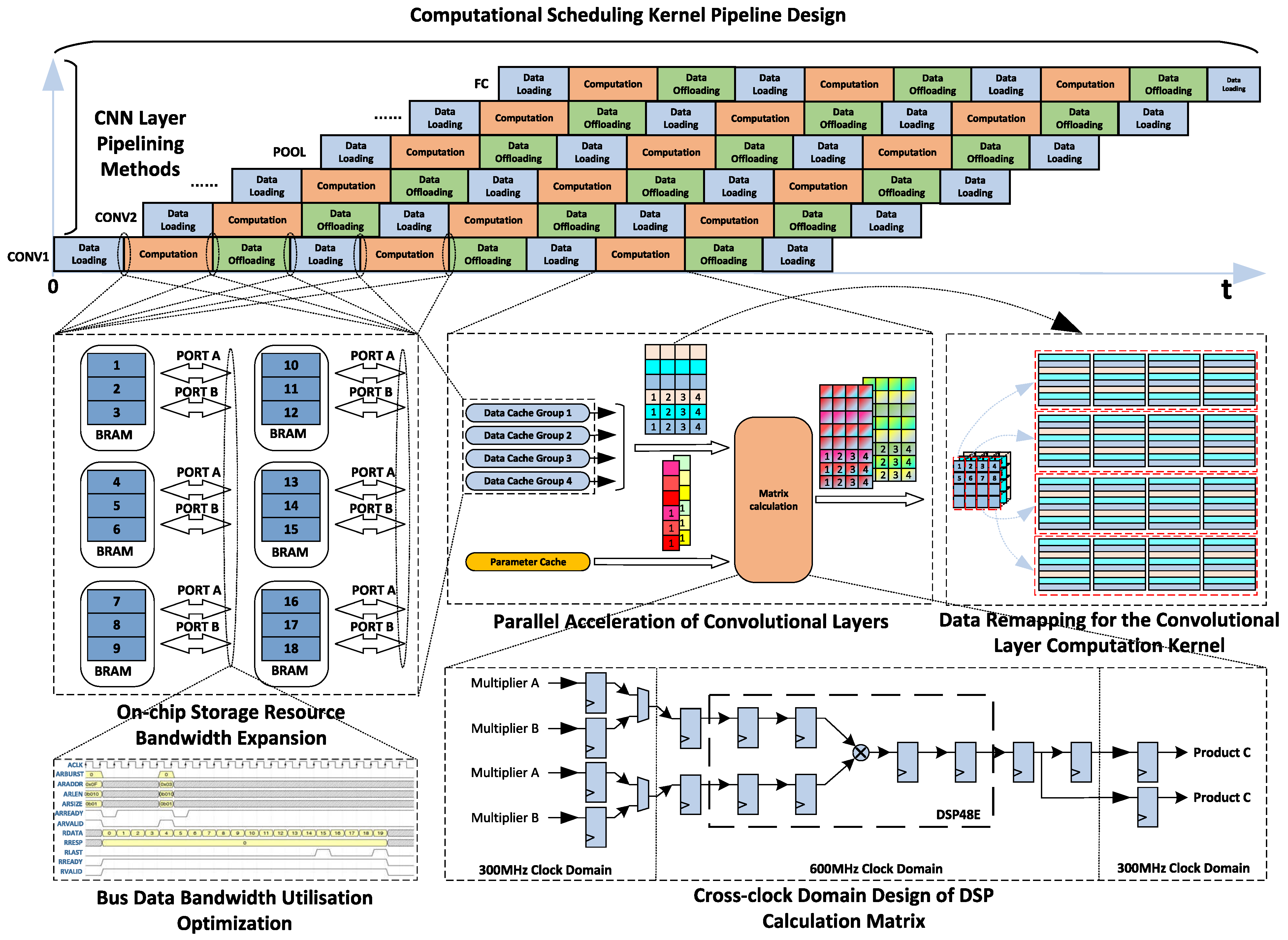
In order to solve the problem of consistency of arithmetic power, speed, and resources, we make full use of the characteristics of FPGAs in the proposed architecture and adopt a comprehensive optimization method of computation, timing, and resources for the CNN model, using multi-channel parallelization to improve the arithmetic power, using scheduling tasks and intensive computation pipelining to meet the data bandwidth requirements of the algorithm, and uniformly scheduling the speed and area of the calculation matrix to save hardware resources, the full view of the study is shown in Figure 2.

2.1. Parallel Acceleration of Computational Layers in CNN

2.1.1. Parallel Acceleration of Convolutional Layers

The convolutional layer is the most computationally intensive for a general CNN. For an input size of 224 × 224 × 3, convolution with a 7 × 7 × 3 × 64 convolutional kernel is approximately equivalent to the number of input parameters multiplied by the number of convolutional kernel parameters; however, for batch, activation, and pooling layers, the computation is only approximately the size of the input size itself, which is a reduction in computation by thousands of times compared to convolutional layers. Therefore, the design of the acceleration core for CNN needs to focus on the acceleration scheme of the convolutional layer.
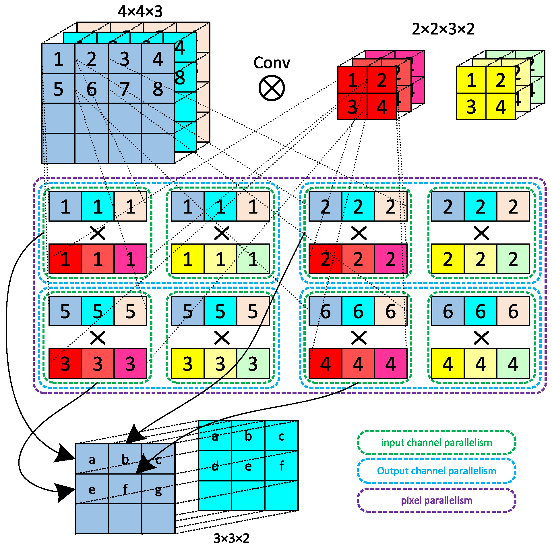
As shown in Figure 3, taking the example of a convolution operation between a 4 × 4 × 3 input tensor and a 2 × 2 × 3 × 2 convolution kernel, the parallel acceleration of the convolution layer is divided into three main dimensions: input channel parallelism, output channel parallelism, and pixel parallelism.
Input channel parallelism is the parallelization of the product of the input tensor and the convolution kernel. The results are added together to obtain a pixel of the output channels. Input channel parallelism calculates the channel vector of one pixel of the input tensor and one pixel of the convolution kernel in a dot product operation each time and finally adds up the results. The hardware implementation of this operation requires the logic to access all channels of the input vector and the convolution kernel simultaneously, so the bit width of the computational kernel needs to be adjusted accordingly. For example, for a kernel with eight input channels in parallel, a single data transfer from the kernel requires 8× the data bit width. If the number of input channels is less than 8, the rest of the bit widths are complemented by 0. Suppose the number of input channels exceeds 8; only eight are counted in each computation. The computation is divided into multiple computations, complementing the last by 0.
Output channel parallelism refers to the simultaneous convolution of an input tensor with multiple convolution kernels to obtain multiple channels of the output tensor. This operation does not increase the bandwidth requirement of the computational kernel for the input data. However, it requires the computational kernel to be able to access the values of the convolution kernel on multiple output channels at the same time.
Pixel parallelism means that the elements of the input tensor at different positions are convolved with the convolution kernel. In contrast, the elements of the output tensor at different positions are obtained in parallel. Take the example of a 4 × 4 × 3 input tensor and a 2 × 2 × 3 × 2 convolution kernel. Assuming the top-left corner of the input tensor is 1, the pixel values in the first row of the output tensor are obtained by simultaneously computing the convolution of the pixels in positions 1, 2, and 3 with the convolution kernel. This operation requires simultaneous access to the element values of the input channel at different pixel points. It requires a hardware design that increases the access bandwidth of the computational kernel. For example, in a parallel scheme with a pixel parallelism of 4, the input tensor is divided into different data buffer groups by column. The number of pixels in parallel is complemented by 0. As a result, the pixel values read by the computational kernel are located in different buffer groups during the entire convolution operation, thus increasing the access bandwidth of the computational kernel.
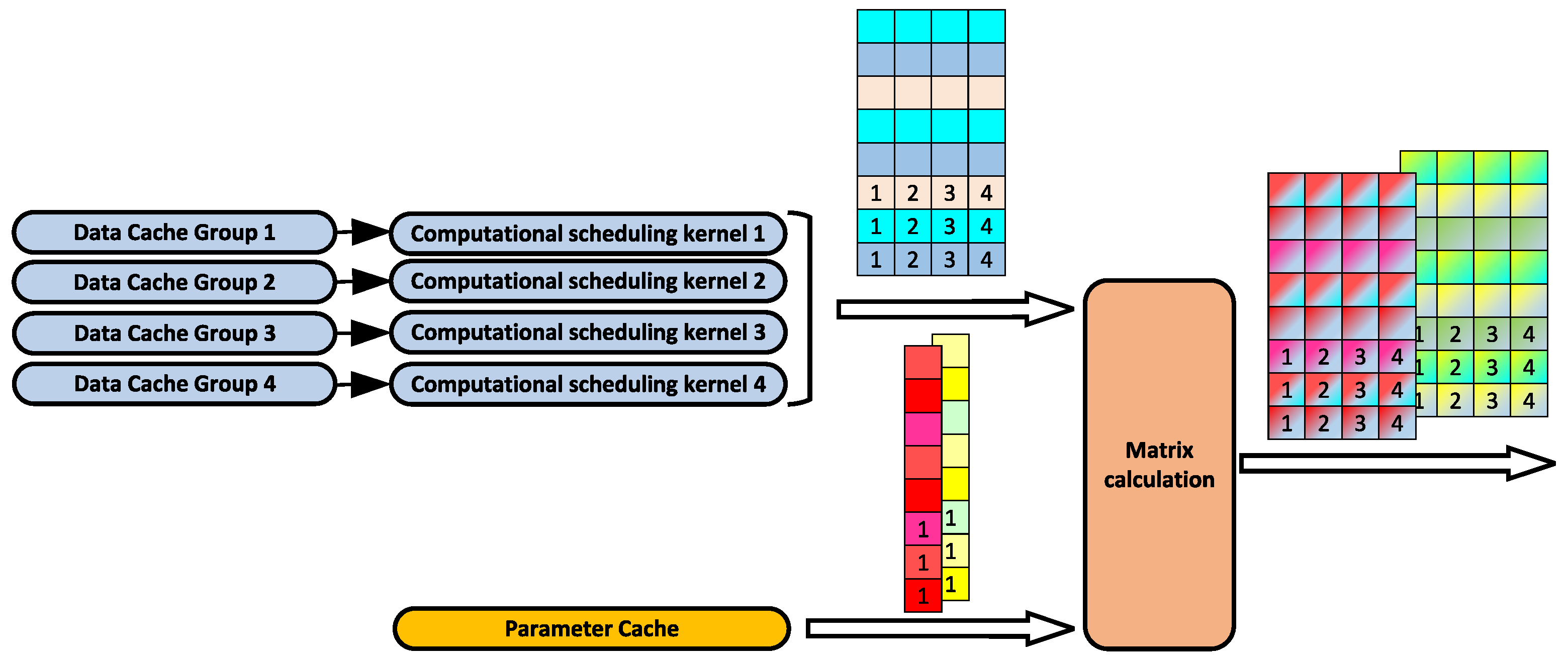
As shown in Figure 4, the similar scheme used is eight-input parallelism, eight-output parallelism, and four-pixel parallelism. The computational kernel can compute 256 multiplication and addition operations in a single clock, i.e., 512 operations. The computational kernel is intended to run at a minimum of 300 M, giving a computational power of 153.6 GOPS. The accelerator will be able to run the 2 GOPS detection model TinyYOLO in real-time.

2.1.2. Parallel Acceleration of Pooling Layer and Fully Connected Layer

Compared to the convolutional layer, the pooling layer does not need to be loaded with parameters. The computational effort and bandwidth of the accessed data are significantly reduced, so only a reasonable parallel computation needs to be planned. The TinyYolo model used in this paper contains only MaxPooling of size 2 × 2, so the parallel loop is designed as follows:
  • The mapping strategy of the input data remains unchanged compared to that of the convolutional layer, using input channel parallelism plus pixel parallelism so that the pooling layer computational kernel accesses eight input channels and four pixels at the same time.
  • The pooling layer differs from the convolutional layer in that the convolutional layer needs to iterate through the length and width of the convolutional kernel on a pixel. In contrast, the pooling layer must only iterate through each pixel once. Therefore, after reading 4 pixels of data in this paper, we change rows and read 4 pixels in the second row. After two reads of 2 × 4 pixels, the maximum value in the channel is taken, and the data of the two output pixels is obtained. The specific pooling layer parallelism method is shown in Figure 5.
The input data of the fully connected layer is 1 × 1 in length and width. However, the number of input channels is generally more significant. The number of parameters needed for computation is multiplied by the number of output channels, making the number of parameters much larger than that of the convolutional layer. In this paper, we adopt a similar approach to the partial loading of convolutional layers by partially loading the parameters of the fully connected layer and loading only one or a few output channels at a time to reduce the need for on-chip BRAM. The computational scheduling kernel transfers the input data and weights to the external computation matrix in parallel. The FPGA’s on-chip DSP performs the multiplication operation between them and then returns them to the computational scheduling kernel for accumulation.

2.1.3. Data Remapping for the Convolutional Layer Computation Kernel

In order to match the high parallelism of the computational kernel and to avoid the underutilization of the computational parallelism caused by the lack of access memory bandwidth, this paper remapped the data and parameters. It changed the data arrangement to ensure that the computational kernel can read the data for computation at the same time. This paper uses an architecture with eight parallel inputs, eight parallel outputs, and four parallel pixels. The data input required for the convolution kernel is the parallel input number 8 × pixel parallel number 4, the parameter input required is the output parallel number 8, the quantization of both data and parameter is a 16bit fixed point, the actual data remapping scheme used is shown in Figure 6.
In this paper, eight 16-bit data are combined into one word (WORD), which is used to temporarily store data and parameters with the same BRAM bit width and word length of 128 bits so that the computational kernel can access eight data in parallel on the channel at the same time. If the number of input channels is greater than 8, the data of subsequent input channels are stored incrementally on the address. If the number of channels is not a multiple of 8, the high bits are complemented by 0 to simplify the data reading operation. A pixel stores all input channel data for output channel 1, then all input channel data for output channel 2, and so on. The computational kernel can access the parameter data of eight output channels simultaneously. The pixel parallel data access to the input data is implemented as in Figure 7.
In addition to channel remapping, the input data is also remapped within rows according to the number of pixels in parallel and stored in different BRAMs. In this paper, for example, the data in each row is grouped by the remainder of 4, i.e., column 0, column 4, etc. column 1, column 5, etc., and so on. If the number of columns is not a multiple of 4, simplify the data reading operation by a multiple of 4. By storing the data in groups 1 to 4 in BRAMs, the convolutional computational kernel has four access ports and can access the data in four BRAMs simultaneously.
The computation unit must perform a Width × Height × Depth × Channel calculation for each input pixel within a single convolutional layer calculation. In this paper, the computational kernel takes the data of 8 input channels of 4 pixels, multiplies and adds the data of 8 input channels of the first pixel of the convolution kernel, then iterates through the input channels, then shifts the whole input data window right by one pixel, multiplies and adds the data of the second pixel of the convolution kernel until the result of one output channel is obtained, and finally iterates through the output channels, after this round of computation, we get the result of the convolution of the 4 pixels in all output channels.
Considering the TinyYolo model, the batch layer and the Rectified Linear Unit (ReLU) layer are both after the convolutional layer; this paper integrates the batch layer and the activation layer with the convolutional layer in the processing flow so that, in practice, only the results can be manipulated before the output data of the convolutional kernel, avoiding reloading data and parameters and reducing data access requirements.
Due to a large number of parameters and the large amount of data in a single convolutional layer, the BRAM memory size may be exceeded, and the direct reading of the Dynamic Random Access Memory (DRAM) may cause high read latency and reduce the efficiency of the computation. Therefore, only a part of the data or parameters can be loaded simultaneously. Then another part can be loaded after one calculation until the convolutional layer is completed. The data within the layer is divided according to the pixel location of the data, and each part of the data is divided by a multiple of the total length and width to reduce the number of cycles.
Parallel acceleration of computational layers in CNN decomposes the computational process of CNN models in three dimensions: input channel, output channel, and pixel. Parallel acceleration of these dimensions significantly improves the efficiency of the CNN algorithm. Traditional methods focus on the computational level of convolutional operations and do not improve enough on the structural level of the algorithm.

2.2. Computational Scheduling Kernel Pipeline Design

2.2.1. Convolutional Layer, Pooling, Fully Connected Layer Pipelining Methods

This paper uses High-Level Synthesis Tool (HLS) pipeline and unroll methods to constrain the loops within the scheduling kernel, the software code is synthesized into pipelined hardware logic to improve computational efficiency.
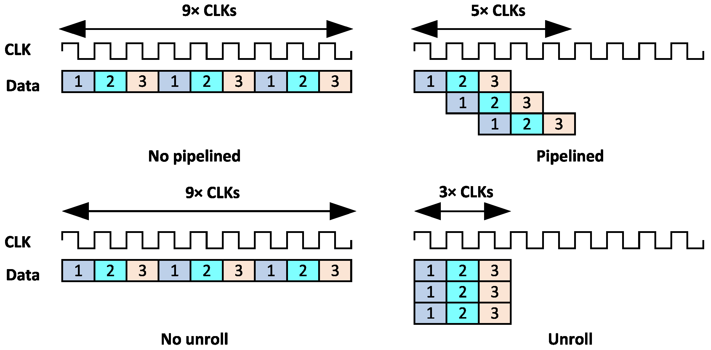
As shown in Figure 8, the pipelined approach shortens the initial interval of hardware execution so that a common computational logic between loops can implement different computational steps within a loop. An unpipelined HLS logic has an initial interval equal to the number of clocks, which takes three clocks to execute a round of computation. The second loop starts three clocks from the start of the first loop, so the initial interval is 3. The total time taken to complete the function is reduced from 9 clocks to 5 clocks, resulting in a significant increase in computational efficiency. The HLS unroll constraint allows operations within a loop to be executed separately so that operations with different loop counts can be performed simultaneously. Unroll requires the HLS to instantiate a finite number of hardware logic units for computation, the upper bound of the loop to be parallelized must be fixed and known at the time of synthesis. Therefore, in this paper, the number of parallelisms is set to a constant for each of the three levels of parallelism, input channel parallelism, output channel parallelism, and pixel parallelism, so that the HLS can perform the computation correctly in parallel. Compared to pipelining, parallelization takes less time but consumes three times more resources and requires no logical dependencies between loops. For example, if the second loop needs to use the result of the first loop, only pipelined logic can be used, not parallelized logic. All loops within the pipeline bound loop are parallelized, using parallel logic to implement the computation within the loop.
In order to improve the overall efficiency of the acceleration core, the convolutional, pooling, and fully connected layers are all designed with independent pipelines at an initial interval of 1 to maximize the use of parallel computation units and data throughput bandwidth. The loop logic of the convolutional layer is the most complex of the three computations, and its loop nesting is shown in Algorithm 1.
Algorithm 1: Convolutional layer loop nesting algorithm
 1:for each i n p u t _ r o w _ i t e r [ 0 , I N P U T _ R O W _ R O U N D ]  do
 2:    / / loop level 1
 3:    / / the traversal of the number of rows of the input tensor
 4:   for each i n p u t _ c o l _ i t e r [ 0 , I N P U T _ C O L _ R O U N D ]  do
 5:      / / loop level 2
 6:      / / the traversal of the number of columns of the input tensor
 7:     for each o c p _ r o u n d [ 0 , O C P _ R O U N D ]  do
 8:         / / loop level 3
 9:         / / the traversal of the number of the output channels
 10:        for each i t e r _ r o w [ 0 , K E R N E L _ W H ]  do
 11:           / / loop level 4
 12:           / / the traversal of the convolution kernel tensor rows
 13:          for each i t e r _ c o l [ 0 , K E R N E L _ W H ]  do
 14:              / / loop level 5
 15:              / / the traversal of the convolution kernel tensor columns
 16:             for each i c p _ r o u n d [ 0 , I C P _ R O U N D ]  do
 17:                / / loop level 6
 18:                / / the traversal of the convolution kernel input channels
 19:               #pragma HLS pipeline
 20:               for each i t e r _ p p [ 0 , P P ]  do
 21:                   / / loop level 7
 22:                   / / loops of pixel parallelism
 23:                  for each i t e r _ o c p [ 0 , O C P ]  do
 24:                     / / loop level 8
 25:                     / / loops of output channel parallelism
 26:                    for each i t e r _ i c p [ 0 , I C P ]  do
 27:                        / / loop level 9
 28:                        / / loops of input channel parallelism
 29:                    end for
 30:                  end for
 31:               end for
 32:             end for
 33:          end for
 34:        end for
 35:     end for
 36:   end for
 37:end for
Loop level 1 represents the traversal of the number of rows of the input tensor. Loop level 2 represents the traversal of the number of columns of the input tensor. For example, suppose the number of parallel pixels is 4. In that case, the loop level means that after each round of convolution, the pointer is shifted 4 pixels to the right until the traversal of a row is completed. Loop level 3 represents the traversal of the number of output channels. Loop levels 4 and 5 represent the traversal of the convolution kernel tensor rows and columns, respectively. Loop level 6 represents the traversal of the convolution kernel input channels. Loops 7, 8, and 9 are loops of pixel parallelism, input channel parallelism, and output channel parallelism, respectively. Loops 1–6 use the pipeline constraint, which means that these loops will be combined into one big loop, and the upper limit of the big loop is the product of the upper limit of all small loops. Loops 7–9 below the pipeline constraint are constrained to be unrolled loops. Within a convolutional operation, the computation scheduling kernel iterates through all the elements of the output tensor by loops 7–9, computes one of the element values by loops 4–6, and unrolls the convolutional operation in parallel by loops 1–3 to improve the computational efficiency and finally obtain the result of a whole convolutional layer.
As shown in Algorithm 2, the pooling layer does not need to consider input channel parallelism compared to the convolutional layer since the number of input channels is the same as the number of output channels. Only the output channels need to be parallelized. Loop level 1 represents the traversal of the input tensor row direction. Loop level 2 represents the traversal of the input tensor column direction. Loop level 3 is the traversal of the output channels. Loop level 4 is the traversal of the pooling range in the row direction. Loop 5 is the traversal of the pooling range in the column direction. Loops 6 and 7 are for pixel and output channel parallelism, respectively. Loops 1 and 2 in the pooling layer traverse the output tensor, and each element of the output tensor corresponds to the maximum value of the pooling range in the input tensor; loops 4 and 5 are the traversal of the pooling range, and loops 6 and 7 are parallel acceleration.
As shown in Algorithm 3, Considering TinyYolo’s 17th fully connected layer, with an input tensor of 1 × 1 × 50,176 and an output tensor of 1 × 1 × 256, the fully connected layer parameter of 1 × 1 × 50,176 × 256 is the most significant layer in the entire network. Suppose the output channels are parallelized like the convolutional layer, the fully connected layer must load at least 50,176 times the number of output channels in parallel with 16-bit fixed-point parameters, which takes up a lot of on-chip BRAM storage resources. Therefore, in this paper, the fully connected layer includes only two dimensions: input channel and pixel parallelism. The loop level 1 of the fully connected layer traverses the input tensor channels. Loop level 2 traverses the output tensor channels. Loop levels 3 and 4 are pixel parallelism and input channel parallelism, respectively.
Algorithm 2: Pooling layer loop nesting algorithm
 1:for each i n p u t _ r o w _ i t e r [ 0 , I N P U T _ R O W _ R O U N D ]  do
 2:    / / loop level 1
 3:    / / traversal of the input tensor row direction
 4:   for each i n p u t _ c o l _ i t e r [ 0 , I N P U T _ C O L _ R O U N D ]  do
 5:      / / loop level 2
 6:      / / traversal of the input tensor column direction
 7:     for each o c p _ r o u n d [ 0 , O C P _ R O U N D ]  do
 8:         / / loop level 3
 9:         / / traversal of the output channels
 10:        for each i t e r _ r o w [ 0 , K E R N E L _ W H ]  do
 11:           / / loop level 4
 12:           / / traversal of the pooling range in the row direction
 13:          for each i t e r _ c o l [ 0 , K E R N E L _ W H ]  do
 14:              / / loop level 5
 15:              / / traversal of the pooling range in the column direction
 16:             #pragma HLS pipeline
 17:             for each i t e r _ p p [ 0 , P P ]  do
 18:                / / loop level 6
 19:                / / pixel parallelism
 20:               for each i t e r _ o c p [ 0 , O C P ]  do
 21:                   / / loop level 7
 22:                   / / output channel parallelism
 23:               end for
 24:             end for
 25:          end for
 26:        end for
 27:     end for
 28:   end for
 29:end for
Algorithm 3: Fully connected layer loop nesting algorithm
 1:for each i n p u t _ d _ i t e r [ 0 , I N P U T _ R O W _ R O U N D ]  do
 2:    / / loop level 1
 3:    / / traverses the input tensor channels
 4:   for each o u t p u t _ d [ 0 , O U T P U T _ D ]  do
 5:      / / loop level 2
 6:      / / traverses the output tensor channels
 7:     #pragma HLS pipeline
 8:     for each i t e r _ p p [ 0 , P P ]  do
 9:         / / loop level 3
 10:         / / pixel parallelism
 11:        for each i t e r _ i c p [ 0 , I C P ]  do
 12:           / / loop level 4
 13:           / / input channel parallelism
 14:        end for
 15:     end for
 16:   end for
 17:end for

2.2.2. On-Chip Storage Resource Bandwidth Expansion

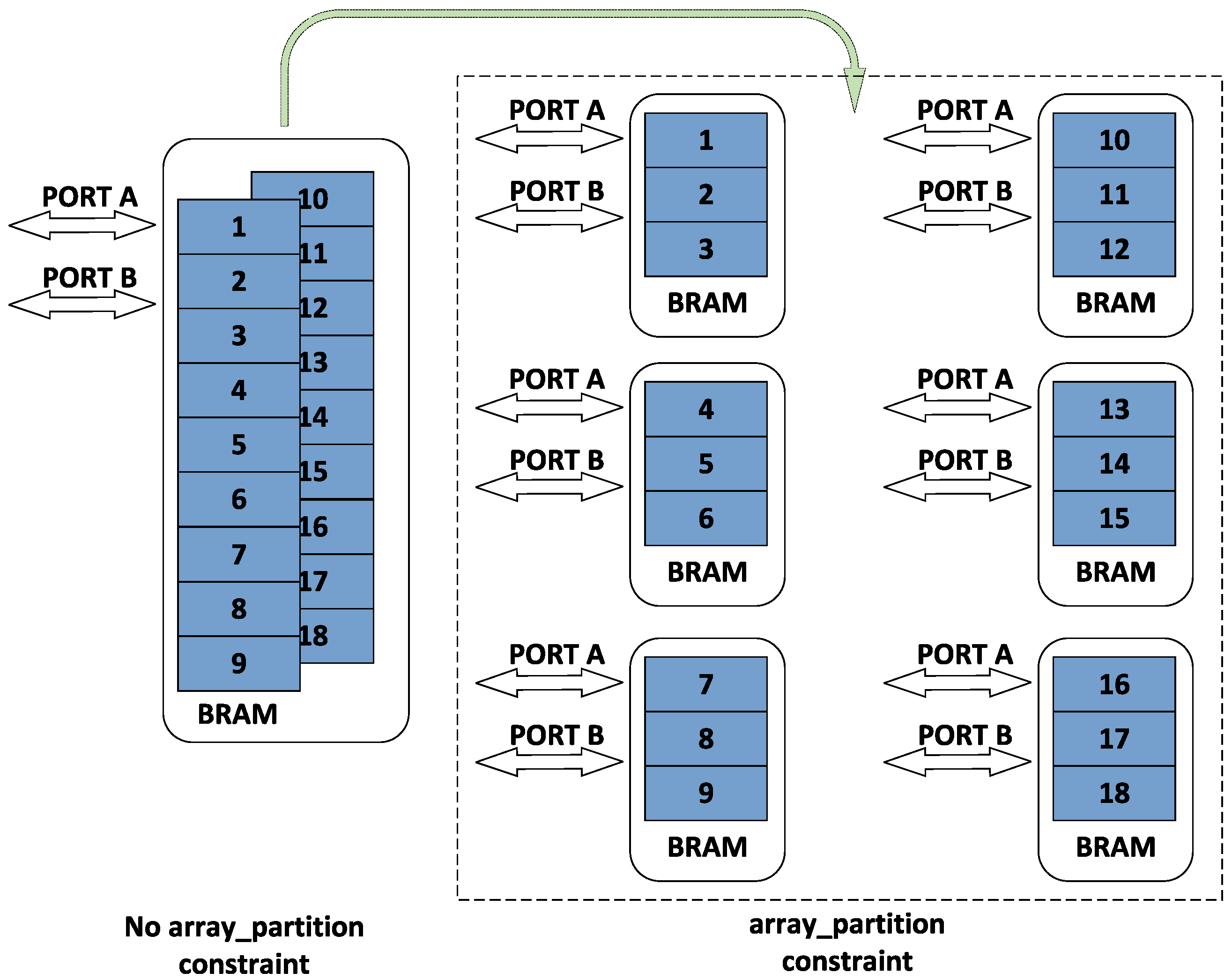
In the acceleration core, the convolutional scheduler needs to read a number of the input channel parallelism × output channel parallelism parameters per clock, which are preloaded by the parameter loading kernel through the AXI bus into the BRAM. In response, the Xilinx HLS tool provides an array_partition constraint to break the BRAM into smaller sub-BRAM cells with more interfaces to guarantee access bandwidth. The specific role of the array_partition constraint is shown in Figure 9.
A BRAM capable of storing nine words is instantiated into three BRAMs capable of storing three words after a memory decomposition constraint of factor 3, which expands the access bandwidth of the memory to three times the original one. In this paper, since the convolutional scheduling kernel needs to access the input channel parallelism × output channel parallelism, and the BRAM bit width is 16 bits × input channel parallelism, the storage decomposition factor is equal to the output channel parallelism number 8, thus decomposing one BRAM into 8 in parallel on the output channel so that the scheduling kernel can access all the required parameters simultaneously.

2.2.3. Partial Loading and Partial Calculation of Data within Layers

Due to the limited on-chip BRAM storage space, the data and parameters cannot be simultaneously loaded into the data storage area. If the data is accessed directly from DRAM, it will greatly slow down the operation efficiency of the acceleration core. Considering that the output of the convolutional layer and the fully connected layer is independent, the acceleration core designed in this paper adopts a partial loading and partial computation strategy, splitting the independent data and only computing the loaded data in each computational kernel inference, then storing the output data in the DRAM. The output data is then stored in the DRAM at the corresponding location to reassemble the output into a complete computational layer.
On-chip storage includes the parameter buffers, the data loading buffers, and the data storage buffers, which must be treated separately. If the storage space is too large, it will take up too many BRAM resources on the FPGA, affecting the potential of the acceleration core to scale parallelism for more computationally intensive models; if the storage space is too small, the on-chip BRAM will not be able to load the input data required at a time. This situation would increase the bandwidth requirements of the acceleration core and increase unnecessary parameter loading time. Considering that the input tensor size of the FC17 layer in the TinyYolo network is 1 × 1 × 50,176, which requires the most significant data load buffer with a depth of 6272 at 128 bit width, this paper sets the data loading buffer bits in depth to 2048 × 4. In addition, the data storage buffer is 128 bits in width and 8192 bits in depth, and the parameter storage is 128 bits in width and 2048 bits in depth. This paper shows the partial loading strategy for each layer of the TinyYolo network inference in Table 1.
As seen from Table 1, the parameter buffers, the data loading buffers, and the data storage buffers were not overflowed during the inference process of the whole TinyYolo network by the partial loading and partial computing strategy, and the BRAM resource consumption of the whole acceleration core is kept within a reasonable range.
In order to make the access bandwidth of data meet the arithmetic power requirement of the CNN algorithm after being accelerated, the access method of data must be specially designed, for which we propose three methods: data streaming, BRAM expansion, and partial calculation, which can significantly improve the matching requirement of data and arithmetic power so that the CNN algorithm can execute almost at total capacity. Traditional methods have yet to be studied in this area.

2.3. Bus Access and DSP Resource Optimization Strategies

2.3.1. Bus Data Bandwidth Utilisation Optimization

The AXI bus is an on-chip bus protocol defined by ARM. The AXI4 bus used in this document includes AXI4-LITE, AXI4-STREAM, and AXI4-MM. AXI4-MM is an AXI4 protocol used for efficient data interaction with memory cells. In this paper, the data loading kernel, data unloading kernel, and parameter loading kernel all use the AXI4-MM protocol to interact with DRAM efficiently.
In order to utilize the data transfer bandwidth of the AXI-MM bus as much as possible and increase the data throughput, this paper optimizes the utilization of the AXI-MM bus in three ways:
  • Using Burst mode increases data access and reduces the number of clocks occupied by handshaking and transferring.
  • Using Outstanding mode to increase the number of reads and write, which AXI host can launch before blocking.
  • Increasing the pipeline length to avoid the pipeline blocking caused by the AXI-MM read and write instructions not returning.
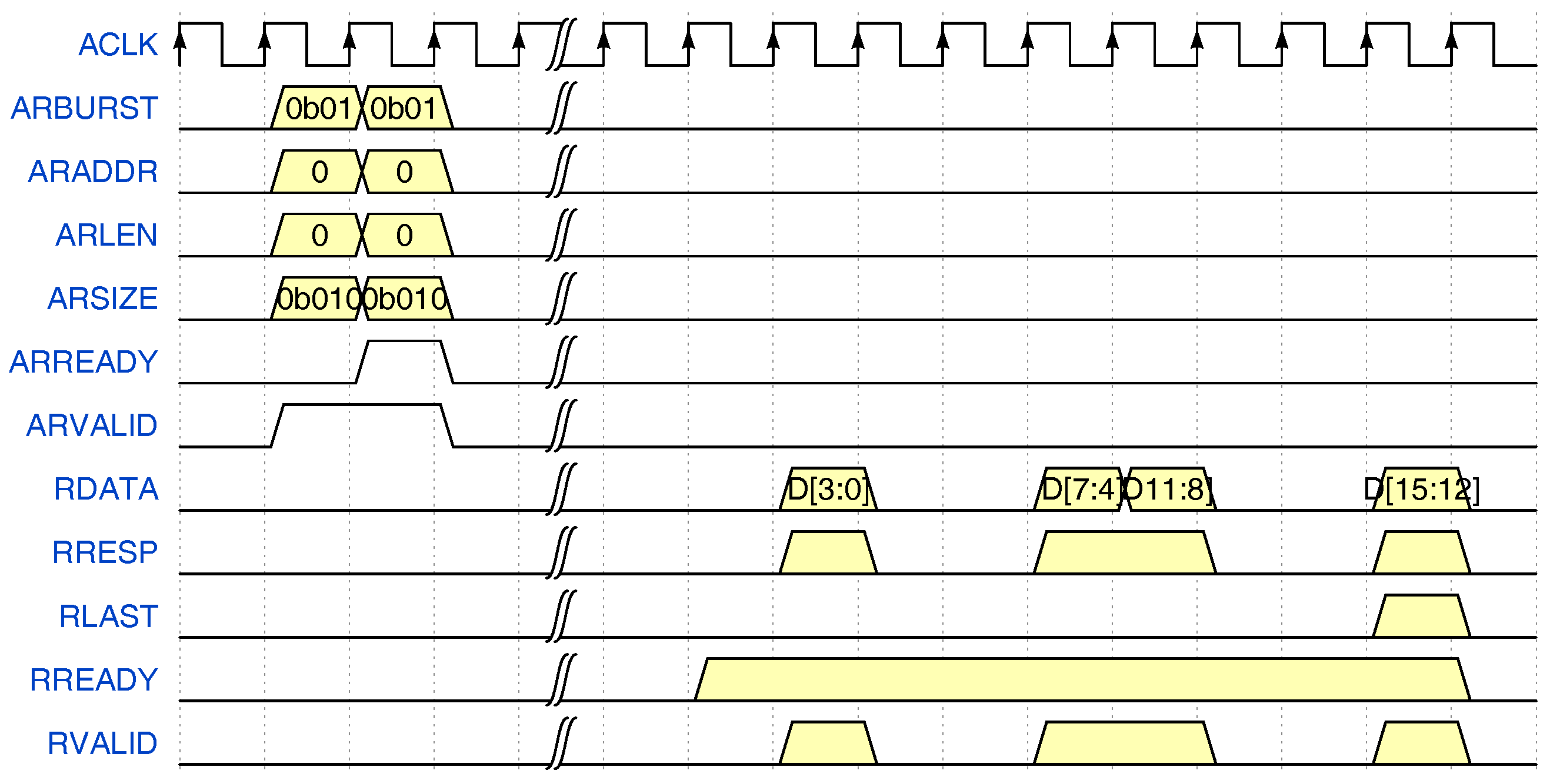
The burst mode of AXI-MM can reduce the number of reads or write commands initiated by a data access to DRAM by packaging multiple accesses on a single memory address into multiple accesses to data on consecutive addresses. In this paper, since the AXI-MM interfaces are all connected to the same Processing System (PS) HP (High Performance) interface through the AXI interconnect. Burst mode reduces the number of conflicts between the kernels. The timing diagram of the AXI burst mode is shown in Figure 10.
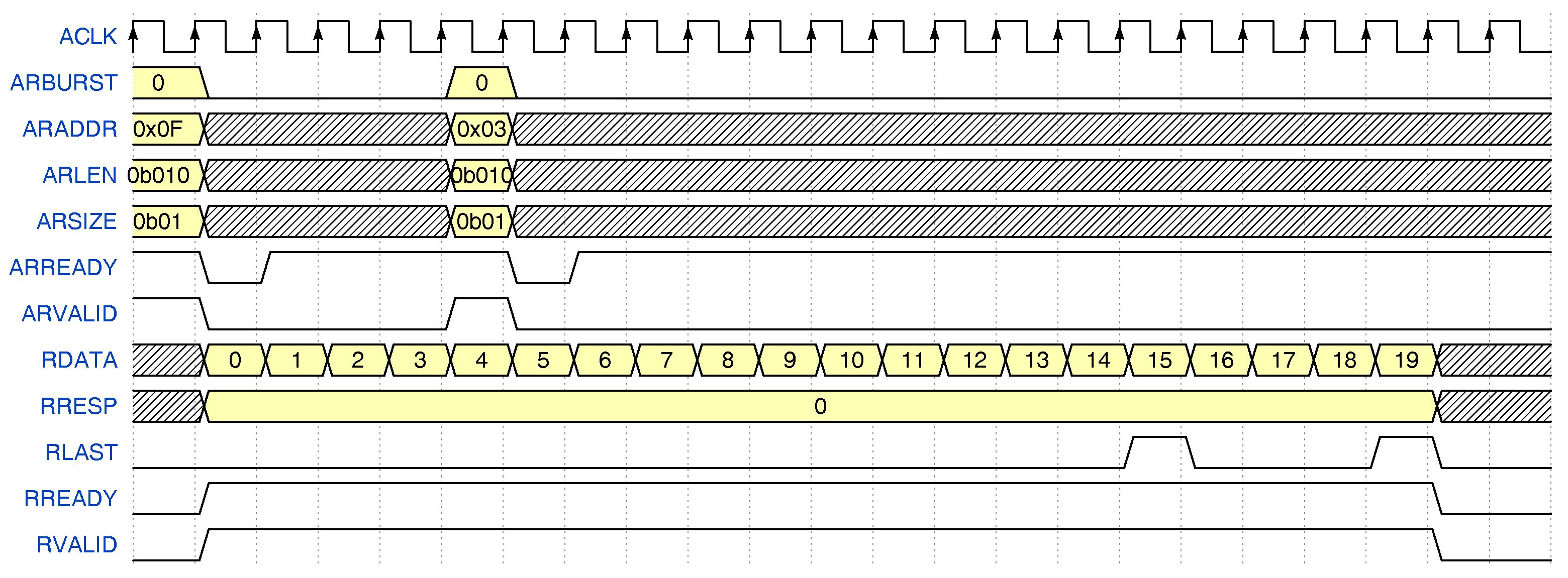
The outstanding mode gives the AXI-MM host a data buffer, which allows the host to make several requests without blocking. The outstanding mode data buffer length is the outstanding number × the maximum burst length × the word length. An excessive outstanding number can lead to crowding too many on-chip storage resources. Considering the storage resource consumption and AXI bus utilization, this paper’s outstanding number is 8. The timing diagram for multiple consecutive read commands from the host in outstanding mode is shown in Figure 11.
In the AXI-MM bus access, the slave often needs several or even dozens of clocks to respond to the host’s request. If the length of the pipeline is insufficient, it will reduce the bus utilization and the overall operational efficiency of the module. Therefore, in this paper, the modules interacting with the AXI-MM bus have extended the length of the pipeline by 128 clocks in order to wait for the AXI-MM slave to return data and avoid the host entering a blocking state.
By combining the above three strategies for optimizing the AXI bus utilization, the acceleration core designed in this paper achieves more than 85% utilization of the AXI bus; taking the FC17 as an example, the number of parameters to be loaded in this layer is 50,176 × 256, the theoretical limit time is 5.35 ms, the actual time is 5.90 ms, compared with the time of more than 10 ms before optimization. The AXI bus runs much more efficiently and avoids memory access limitations to accelerate the efficiency of the computation.

2.3.2. Cross-Clock Domain Design of DSP Calculation Matrix

The logic unit for data transfer on the AXI bus often runs at a maximum of 300 MHz. In contrast, the DSP48E core for computing the convolutional layer and fully connected layer multiplication can run at 600 MHz. Therefore, this paper uses a cross-clock domain design with a logic clock of 300 MHz and a DSP48E clock of 600 MHz, so that two multiplication calculations can be multiplexed with a single DSP48E unit. In this paper, with eight input channels in parallel, eight output channels in parallel, and 4 pixels in parallel, 256 fixed-point multiplications are computed per clock, while only 128 DSP48E units are consumed. In order to simplify the data transfer between the 300 MHz base frequency clock and the 600 MHz dual frequency clock, the two clocks are generated using the same 50 MHz input clock through Mixed-Mode Clock Manager (MMCM) or Phase Lock Loop (PLL), and the two clocks are phase aligned. The two clocks generated this way ensure that the frequencies are strictly duplexed. The rising edges are aligned so that the data transferred between them can be steadily transferred by simply passing through the register cache controlled by the two clock domains, eliminating the need for an asynchronous FIFO, saving resources, and simplifying Placing and Routing (PR). Figure 12 shows a diagram of two clocks generated using the same PLL.
The four operands to be multiplied are first buffered in the 300 MHz clock domain using a D flip-flop and then selected by a 600 MHz clock, with the first two operands input at the odd 600 MHz clock and the last two operands input at the even clock. The output of the DSP48E is buffered by two D flip-flops clocked, and the output of the two buffered flip-flops is tapped in the 300 MHz clock domain to obtain a stable output with no sub-stability and convergence in timing. The above architecture works on a pipeline with an initial interval of 1. Each fundamental clock can use one DSP48E to calculate fixed-point multiplication twice, which realizes the time-division multiplexing of DSP48E resources and reduces resource consumption. Cross-clock domain DSP48E unit is shown in Figure 13.
A select signal in the above cross-clock domain design is identical to the 300 MHz clock in the waveform. However, the clock signal is buffered by Global Buffer (BUFG) into the clock network within the FPGA, which provides a stable clock signal for the global flip-flop with low jitter and skew. Since there is no direct path from the clock network to the logic input, the 300 MHz clock cannot be used as the select signal. We use a clock follower to generate the select signal. The diagram of the clock follower and the output waveform of each point are shown in Figure 14.
The DSP resources inside the FPGA are limited. Our proposed method takes advantage of the strategy of doubling the computational efficiency in the high-speed clock domain through a time-for-space approach to achieve the same computational efficiency with fewer DSPs and specifically optimizes the access for the AXI bus operation timing so that the bus can work almost at total capacity. Compared with the traditional method, we use fewer DSP resources to do the same work or the same DSP resources to do twice the work.

3. Results and Discussion

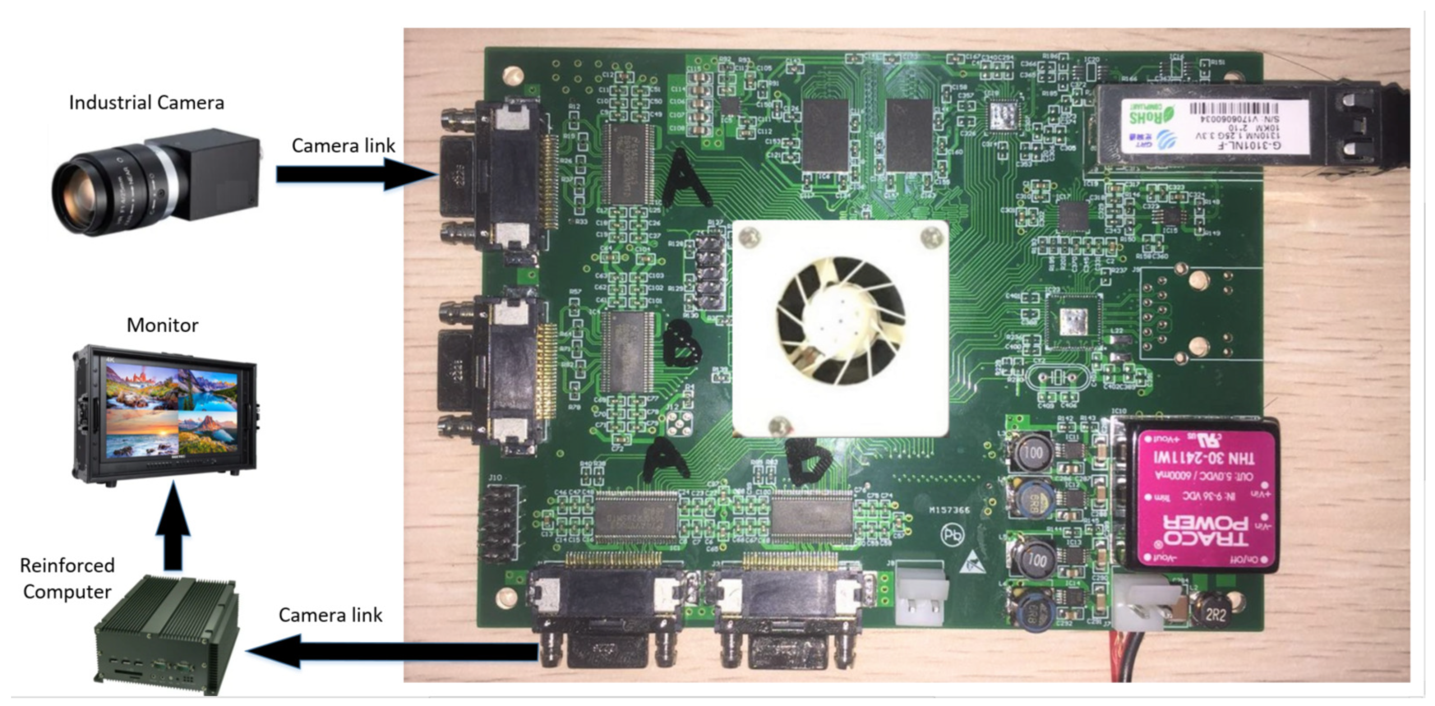
To verify the generality and effectiveness of our deep learning acceleration core architecture, we used the Xilinx ZU15EG chip to build a heterogeneous video processing system. The PL side of the ZU15EG chip includes 26.2 Mb of on-chip storage resources, 3528 DSP48E2, and four external DDR4 chips on the PS side, with a maximum theoretical transfer bandwidth of 38.4 GB/s. This paper’s data transfer bus is connected to the same AXI4 HP interface at 300 MHz, 128 bit width, and 4.8 GB/s theoretical maximum bandwidth. Therefore, the on-chip DDR bandwidth is sufficient to support the data transfer bandwidth required for neural network computing. In addition, the input data for this paper comes from a real-time input video stream, so the hardware platform is equipped with a camera link chip for accessing the real-time video stream. The input video is processed by the interface chip, waiting for the acceleration core to infer. The detected results are sent from the PS to the PL side, overlaying the detected frame on the output video and displaying it through the video interface. The hardware we use is shown in Figure 15. We have used this hardware platform to implement and validate the deep learning acceleration core.
In order to objectively evaluate the ability of our proposed method to handle the consistency problem of arithmetic power, speed, and resources, we make the following assumptions.
  • Our proposed method will not be interrupted by unordered scheduling instructions during network inference tasks, which include parameter updates, recovery after video stream interruptions, and interruption exception handling.
  • The automatic optimization function of the synthesis tool is turned off since we have already performed manual optimization specifically for the proposed method. The secondary optimization of the automatic tool will affect the results.
  • When selecting other methods proposed in the literature for comparison, we try to select FPGA chips of the same architecture system because the internal structure of chips of different architectures is different, which will affect the evaluation of the effect of resource optimization.
In Section 3.1, we illustrate the hardware implementation results and timing of the convolutional and fully connected layer pipelines in the computational scheduling kernel, list the hardware resources consumed by the computational scheduling kernel, and discuss the resource usage. In Section 3.2, we list the hardware resources consumed by the deep learning acceleration core and discuss the resource usage. In Section 3.3, we illustrate the actual performance of the deep learning acceleration core, compare it cross-sectionally with other similar lightweight acceleration cores, and discuss our method’s advantages.

3.1. Computational Scheduling Kernel Implementation and Validation

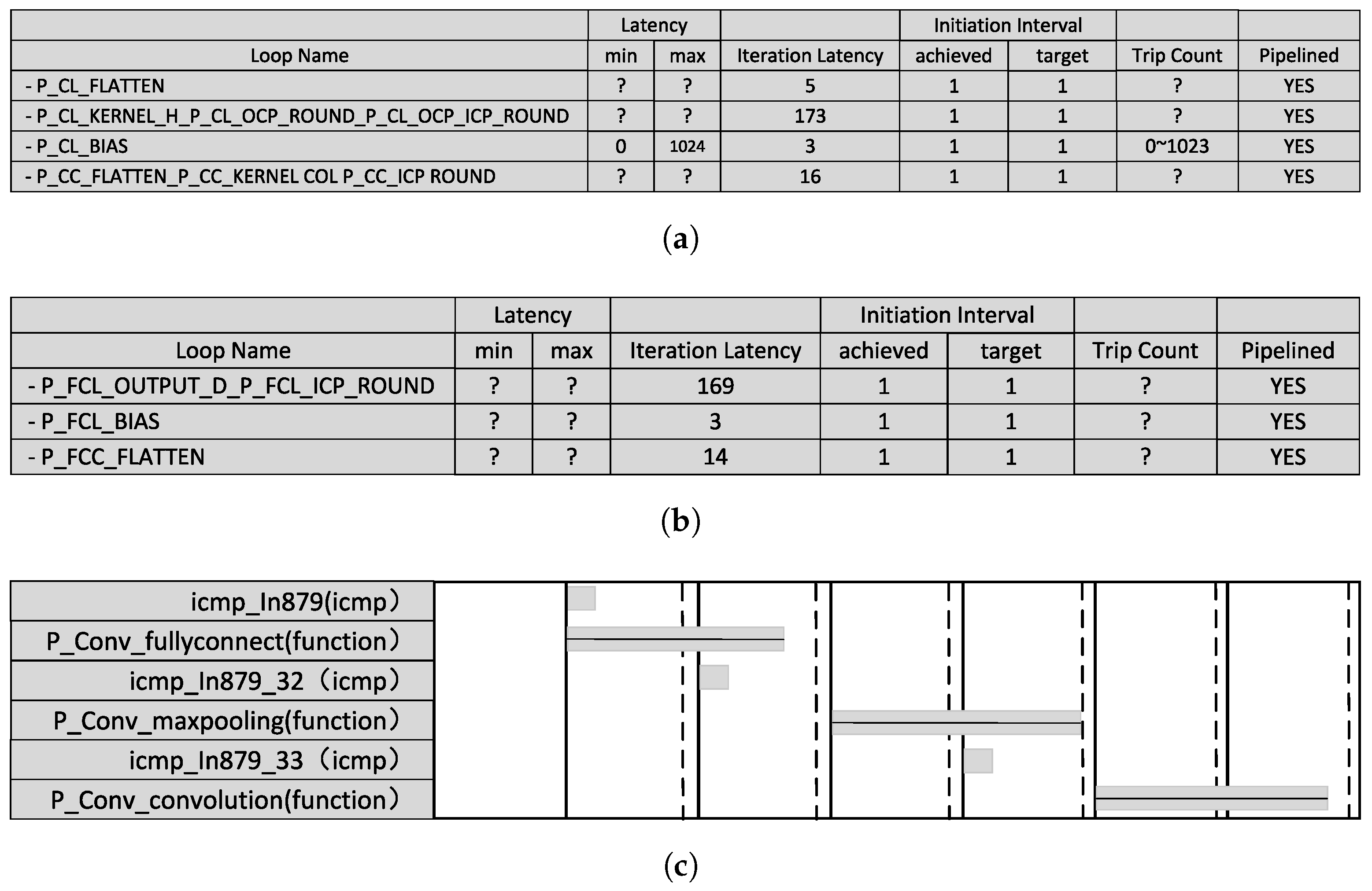
The computational scheduling kernel designed in this paper includes the computation of the convolutional layer, the pooling layer, and the fully connected layer, where the convolutional layer contains four pipelines: Pipeline 1 is the loading pipeline for the parameter data when the number of output channels is equal to the output tensor channels during partial computation, Pipeline 2 is the loading pipeline for the parameter data when the number of output channels is not equal to the output tensor channels during partial computation, Pipeline 3 is the loading pipeline for the bias data in the batch layer, Pipeline 4 is the main pipeline for reading the data stored on the chip and pushing it to the computation matrix to get the result of the convolutional layer. All four pipelines have an initial interval of 1 to maximize computational efficiency and data throughput. The pipeline length of pipeline 2 is 173 because when the number of output channels of the partial computation is not equal to the number of output channels of the output tensor, the address of the parameter load is not continuous and needs to be cut off into several burst transfers, so the pipeline is lengthened to avoid blocking caused by the untimely return of AXI-MM data, which reduces the efficiency of data reading. The pooling layer has the most straightforward pipeline since it does not require loading parameters, with only one main pipeline for computation and the same initial interval of 1. The fully connected layer contains three pipelines: pipeline one is the fully connected multiplication parameter loading pipeline, pipeline 2 is the fully connected bias parameter loading pipeline, and pipeline 3 is the main pipeline for computing the entire connection. Pipeline experiment results are shown in Figure 16.
The computational scheduling kernel runs at 300 MHz with 3.33 ns per clock cycle. With the HLS pipeline design, the most extended single-cycle instruction takes 2.91 ns, with a timing margin of 0.42 ns, which meets the setup hold time for FPGA operation. The overall resource consumption of the computational scheduling kernel is shown in Table 2.
The convolutional layer consumes the most lookup table and trigger resources, mainly because it needs to compute the accumulation of three dimensions in parallel. In contrast, the fully connected layer only needs to compute the accumulation of two dimensions, input channel parallelism and pixel parallelism. At the same time, the convolutional layer computes data access addresses and loop counts most frequently, which requires partial multiplication, such as calculating the data address of a pixel in the input tensor or calculating the total number of current loops. Hence, the convolutional layer consumes the most DSP resources of the three. Finally, the computational scheduling kernel stores the multiplication and bias parameters for the convolution and fully connected layers in an internal BRAM, with 8 channels, 2048 depth, 128 bit width memory for the multiplication parameters and a 256 depth, 128 bit width memory for the bias parameters, which can support the computation of a maximum 2048 output channel tensor. The parameters are stored in BRAM36k, a 36 bit width, 1024 depth memory cell, consuming 69 BRAM36k and 1 BRAM18k.

3.2. Deep Learning Acceleration Core Implementation and Verification

This paper uses HLS to implement the calculation scheduling and data access core and Verilog HDL to implement the DSP computation matrix across the clock domain. The data loading kernel loads data from the DDR through the AXI bus and stores it in the local cache through the BRAM bus. The computation scheduler kernel interacts with the four BRAM local stores through the BRAM bus and sends the output data to the output cache through the AXI bus. The data storage kernel reads the data from the output cache and stores it in the DDR through the AXI bus. The PS section sends commands to each sub-module through the AXI4-LITE bus to control its operating status and inform the data storage address. The overall resource consumption of the deep learning acceleration core is shown in Table 3.
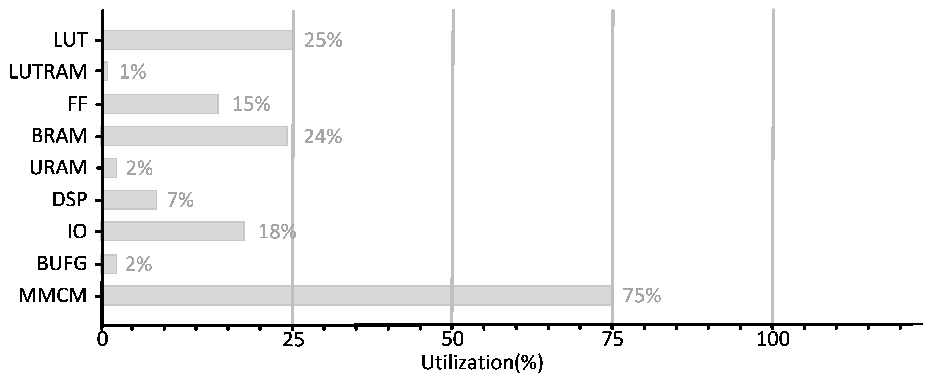
Regarding lookup tables, the computation scheduling kernel consumes a large amount of data, mainly because its function is to remap the data addresses, output the data to the computation matrix, and compute the accumulation of the convolutional layers. The concurrency of the convolutional accumulation is the largest, requiring the sum of 256 fixed points in a pipeline, which consumes many lookup tables. On the one hand, the computation scheduling kernel needs to store many intermediate results. On the other hand, the cross-clock domain processing of the DSP computation matrix needs to use different clock domain triggers to avoid timing problems, which require many trigger cache data. In addition, the DSP consumption of this part is fixed and will not increase due to the parallelism of data computation. In addition to the intermediate data storage, the burst and outstanding modes of the AXI-MM bus require on-chip storage space to cache the data to be sent or received on the bus, which consumes some of the BRAM. In general, the overall resource consumption of the acceleration core architecture is less than 25% of the ZU15EG platform used. In addition to the deep learning acceleration core, the hardware platform also requires a video input and output path. With the addition of these external modules, the overall resource consumption of the hardware platform is shown in Figure 17.

3.3. Performance Analysis of Deep Learning Acceleration Core Inference

The model for acceleration core inference designed in this paper is TinyYolo; the input image is a three-channel image with a resolution of 448 × 448. The output is a 1 × 1470 tensor that includes information on confidence, target frame position, and size. Nineteen layers are included in the TinyYolo model, of which nine layers are convolutional, six layers are 2 × 2 pooling layers, three layers are fully connected, and one layer is an unfolding operation. The total computational volume of the inference is 2.5 GOPS, the number of parameters is 20 M, the parameter data volume is 40 MB for 16 bit quantization, the intermediate result data volume is 11 M, and the data volume is 22 MB for 16 bit quantization. The input and output tensor size, number of parameters, and data volume of each layer are shown in Table 4.
The computational and parametric quantities of the convolutional layer in TinyYolo’s inference are large, so parallel optimization of the convolutional layer is the most important. The acceleration core designed in this paper computes the convolutional layer in parallel with input channel parallel number 8, output channel parallel number 8, and pixel parallel number 4. The computation time of the convolutional layer is shown in Table 5.
The task scheduling pipelining strategy used in this paper is to carry out data loading and storage, and computation simultaneously to avoid data loading and storage affecting the parallel computation efficiency. However, the parameter loading part is inside the computation scheduling kernel. The scheduling kernel cannot compute while loading parameters, so the actual computation time of the convolutional layer is equal to the sum of the parameter loading time and the computation time. The other computational layer in TinyYolo that takes longer to infer, the fully connected layer, has a more significant number of parameters making the parameter loading time longer, and the computational time required to infer TinyYolo once is shown in Table 6.
In addition to the inference time consumed by the convolutional and fully connected layers, the total inference time also includes the data access time of the pooling layer and one input image normalization operation. The acceleration core inference designed in this paper takes 71 ms for the whole network at one time, with an FPS of about 14, which reaches the real-time standard. Considering that in order to optimize the stability of the target detection frame, tracking is generally added after the detection result, a detection result of 14 FPS is sufficient to provide the tracker with a real-time detection result as a tracking target. The theoretical arithmetic power of the acceleration core in this paper is 150 GOPS, and 2.5 G times multiplication and addition are required to infer a TinyYolo, for a total of 5 GOPS of computation, with a theoretical maximum frame rate of 30 FPS and actual computational resource utilization of about 47%. Compared to other designs that use FPGAs to build deep learning acceleration cores, the performance comparison of the acceleration cores in this paper is shown in Table 7.
In this paper, the DSP doubling strategy is adopted. The bus frequency and DSP running frequency are several times higher than other designs, so the acceleration core designed in this paper can guarantee higher computational performance while minimizing DSP consumption and significantly improving the utilization of DSP resources. In Table 7, although different literature uses different hardware platforms and implements other algorithmic models, the parameter Energy Efficiency allows normalizing the performance of different algorithms within the same evaluation system. Our proposed architecture can provide an arithmetic performance of 28.98 GOPS per unit power, which is 20.34% higher than the 2nd place.
Here we have to point out that since our proposed method utilizes a lot of hardware design tricks to optimize specifically for CNN-based models and FPGA structures, it has a good migration capability for algorithms of CNN-based models such as VGG, Multi-scale Residual Aggregation Network (MSRANet), GoogleNet, Inception, Faster R-CNN, etc. For other models, such as Recurrent Neural Networks (RNN) or Generative Adversarial Nets (GAN) models, there is only some optimization capability at the FPGA structure level. Further, since the performance gains in arithmetic power and speed of our proposed deep learning acceleration core rely on highly streamlined and parallelized processing of the hardware, this requires predictable behavior of the inference network because if a random operation interrupts this predictable behavior, such as a parameter update or a bus transfer failure, then all streamlined work has to be restarted, which often results in massive latency. For real-time tasks, this latency is often intolerable.
The test result is shown in Figure 18.

4. Conclusions

This paper proposes an FPGA-based deep learning acceleration core architecture for image target detection, which designs a parallel acceleration scheme to address the problem of arithmetic power, speed, and resource consistency. In this paper, the computational scheduling kernel is streamlined so that the computation unit can perform one parallel computation per clock without waiting for data pre-processing. In order to provide sufficient data access bandwidth for parallel computing units, this paper also designs and implements a three-level data cache architecture of off-chip storage, on-chip storage, and registers, which provides high bandwidth data streams for parallel computing units by slicing on-chip storage to avoid data stream operations affecting the computational efficiency of parallel acceleration cores. Using bus accessing and DSP resource optimization strategies improves bus bandwidth utilization and saves computational resources, reducing the DSP resource to half the original. This paper uses the HLS high-level synthesis tool for deep learning acceleration core development on FPGAs and achieves 14 FPS inference for the TinyYolo model with 5 GOPS computation using less than 25% of the FPGA resource. The acceleration core can run at 30% higher clock frequency, 2–4 times higher arithmetic power, and 28% more efficient DSP resource utilization than other methods. The limitation of this paper is that our proposed parallel acceleration algorithm is only suitable for CNN-based models, and further research on acceleration algorithms for RNN-based or GAN-based models should be conducted in the future.

Author Contributions

Conceptualization, X.Y. and C.Z.; methodology, W.F.; software, X.Y.; validation, X.Y., Z.Y. and Q.W.; formal analysis, C.Z.; investigation, X.Y.; resources, X.Y.; data curation, X.Y.; writing—original draft preparation, X.Y.; writing—review and editing, X.Y. and C.Z.; visualization, X.Y.; supervision, C.Z.; project administration, W.F. All authors have read and agreed to the published version of the manuscript.

Funding

This research was funded by National Natural Science Foundation of China under grant number 61901015.

Institutional Review Board Statement

Not applicable.

Informed Consent Statement

Not applicable.

Data Availability Statement

Not applicable.

Acknowledgments

The authors acknowledge graduate student Xu Yang for his contribution to literature search and collation.

Conflicts of Interest

The authors declare no conflict of interest.

Abbreviations

The following abbreviations are used in this manuscript:
FPGAField Programmable Gate Array
CNNConvolutional Neural Networks
DSPDigital Signal Processing
YOLOYou Only Look Once
Faster R-CNNFaster Region Convolutional Neural Networks
SARSynthetic Aperture Radar
mAPMean of Average Precision
APAverage Precision
ARAverage Recall
UAVUnmanned Aerial Vehicle
RES-YOLOResidual YOLO
GPUGraphics Processing Unit
DSPsDigital Signal Processors
NPUsNeural Processor Units
FPSframes per second
GOPSGiga Operations Per Second
COCOMicrosoft Common Objects in Context
VOCVisual Object Classes
RSRow stationery
VGGVisual Geometry Group
HLSHigh-Level Synthesis Tool
AXI-MMAdvanced eXtensible Interface Memory Map
BRAMBlock Random Access Memory
DRAMDynamic Random Access Memory
HDLHardware Description Language
MCMMMixed Mode Clock Manager
PLLPhase Lock Loop
PRPlacing and Routing
BUFGGlobal Buffer
FIFOFirst Input First Output
DDRDouble Data Rate
HPHigh Performance
PSProcessing System
KNNk-Nearest Neighbor
RNNRecurrent Neural Networks
GANGenerative Adversarial Nets
MSRANetMulti-scale Residual Aggregation Network
LSTMLong Short-Term Memory

References

  1. Redmon, J.; Divvala, S.; Girshick, R.; Farhadi, A. You only look once: Unified, real-time object detection. In Proceedings of the IEEE Conference on Computer Vision and Pattern Recognition, Las Vegas, NV, USA, 27–30 June 2016; pp. 779–788. [Google Scholar]
  2. Ren, S.; He, K.; Girshick, R.; Sun, J. Faster r-cnn: Towards real-time object detection with region proposal networks. Adv. Neural Inf. Process. Syst. 2015, 28, 91. [Google Scholar] [CrossRef] [Green Version]
  3. Sun, B.; Wang, X.; Oad, A.; Pervez, A.; Dong, F. Automatic Ship Object Detection Model Based on YOLOv4 with Transformer Mechanism in Remote Sensing Images. Appl. Sci. 2023, 13, 2488. [Google Scholar] [CrossRef]
  4. Sun, Z.; Leng, X.; Lei, Y.; Xiong, B.; Ji, K.; Kuang, G. BiFA-YOLO: A novel YOLO-based method for arbitrary-oriented ship detection in high-resolution SAR images. Remote Sens. 2021, 13, 4209. [Google Scholar] [CrossRef]
  5. Hu, J.; Zhi, X.; Shi, T.; Zhang, W.; Cui, Y.; Zhao, S. PAG-YOLO: A portable attention-guided YOLO network for small ship detection. Remote Sens. 2021, 13, 3059. [Google Scholar] [CrossRef]
  6. Li, L.; Jiang, L.; Zhang, J.; Wang, S.; Chen, F. A complete YOLO-based ship detection method for thermal infrared remote sensing images under complex backgrounds. Remote Sens. 2022, 14, 1534. [Google Scholar] [CrossRef]
  7. Ye, J.; Yuan, Z.; Qian, C.; Li, X. Caa-yolo: Combined-attention-augmented yolo for infrared ocean ships detection. Sensors 2022, 22, 3782. [Google Scholar] [CrossRef] [PubMed]
  8. Lu, J.; Ma, C.; Li, L.; Xing, X.; Zhang, Y.; Wang, Z.; Xu, J. A vehicle detection method for aerial image based on YOLO. J. Comput. Commun. 2018, 6, 98–107. [Google Scholar] [CrossRef] [Green Version]
  9. Al-Batat, R.; Angelopoulou, A.; Premkumar, S.; Hemanth, J.; Kapetanios, E. An end-to-end automated license plate recognition system using YOLO based vehicle and license plate detection with vehicle classification. Sensors 2022, 22, 9477. [Google Scholar] [CrossRef]
  10. Zhang, Y.; Guo, Z.; Wu, J.; Tian, Y.; Tang, H.; Guo, X. Real-Time Vehicle Detection Based on Improved YOLO v5. Sustainability 2022, 14, 12274. [Google Scholar] [CrossRef]
  11. Liu, M.; Wang, X.; Zhou, A.; Fu, X.; Ma, Y.; Piao, C. Uav-yolo: Small object detection on unmanned aerial vehicle perspective. Sensors 2020, 20, 2238. [Google Scholar] [CrossRef] [PubMed] [Green Version]
  12. Li, Y.; Wang, J.; Huang, J.; Li, Y. Research on Deep Learning Automatic Vehicle Recognition Algorithm Based on RES-YOLO Model. Sensors 2022, 22, 3783. [Google Scholar] [CrossRef] [PubMed]
  13. Chen, L.; Weng, T.; Xing, J.; Pan, Z.; Yuan, Z.; Xing, X.; Zhang, P. A new deep learning network for automatic bridge detection from SAR images based on balanced and attention mechanism. Remote Sens. 2020, 12, 441. [Google Scholar] [CrossRef]
  14. Li, X.; Meng, Q.; Wei, M.; Sun, H.; Zhang, T.; Su, R. Identification of Underwater Structural Bridge Damage and BIM-Based Bridge Damage Management. Appl. Sci. 2023, 13, 1348. [Google Scholar] [CrossRef]
  15. Du, F.; Jiao, S.; Chu, K. Application research of bridge damage detection based on the improved lightweight convolutional neural network model. Appl. Sci. 2022, 12, 6225. [Google Scholar] [CrossRef]
  16. Lin, Y.C.; Chen, W.D. Automatic aircraft detection in very-high-resolution satellite imagery using a YOLOv3-based process. J. Appl. Remote Sens. 2021, 15, 018502. [Google Scholar] [CrossRef]
  17. Madasamy, K.; Shanmuganathan, V.; Kandasamy, V.; Lee, M.Y.; Thangadurai, M. OSDDY: Embedded system-based object surveillance detection system with small drone using deep YOLO. EURASIP J. Image Video Process. 2021, 2021, 1–14. [Google Scholar] [CrossRef]
  18. Jiang, C.; Ren, H.; Ye, X.; Zhu, J.; Zeng, H.; Nan, Y.; Sun, M.; Ren, X.; Huo, H. Object detection from UAV thermal infrared images and videos using YOLO models. Int. J. Appl. Earth Obs. Geoinf. 2022, 112, 102912. [Google Scholar] [CrossRef]
  19. Artamonov, N.; Yakimov, P. Towards real-time traffic sign recognition via YOLO on a mobile GPU. J. Phys. Conf. Ser. 2018, 1096, 012086. [Google Scholar] [CrossRef]
  20. Güney, E.; Bayilmiş, C.; Cakan, B. An implementation of real-time traffic signs and road objects detection based on mobile GPU platforms. IEEE Access 2022, 10, 86191–86203. [Google Scholar] [CrossRef]
  21. Feng, W.; Zhu, Y.; Zheng, J.; Wang, H. Embedded YOLO: A real-time object detector for small intelligent trajectory cars. Math. Probl. Eng. 2021, 2021, 6555513. [Google Scholar] [CrossRef]
  22. Zhang, S.; Cao, J.; Zhang, Q.; Zhang, Q.; Zhang, Y.; Wang, Y. An fpga-based reconfigurable cnn accelerator for yolo. In Proceedings of the 2020 IEEE 3rd International Conference on Electronics Technology (ICET), Chengdu, China, 8–11 May 2020; pp. 74–78. [Google Scholar]
  23. Babu, P.; Parthasarathy, E. Hardware acceleration for object detection using YOLOv4 algorithm on Xilinx Zynq platform. J. Real-Time Image Process. 2022, 19, 931–940. [Google Scholar] [CrossRef]
  24. Xiong, Q.; Liao, C.; Yang, Z.; Gao, W. A Method for Accelerating YOLO by Hybrid Computing Based on ARM and FPGA. In Proceedings of the 2021 4th International Conference on Algorithms, Computing and Artificial Intelligence, Sanya, China, 22–24 December 2021; pp. 1–7. [Google Scholar]
  25. Chen, Y.H.; Emer, J.; Sze, V. Eyeriss: A spatial architecture for energy-efficient dataflow for convolutional neural networks. ACM SIGARCH Comput. Archit. News 2016, 44, 367–379. [Google Scholar] [CrossRef]
  26. Liu, Z.; Dou, Y.; Jiang, J.; Xu, J.; Li, S.; Zhou, Y.; Xu, Y. Throughput-optimized FPGA accelerator for deep convolutional neural networks. ACM Trans. Reconfigurable Technol. Syst. 2017, 10, 1–23. [Google Scholar] [CrossRef]
  27. Peemen, M.; Setio, A.A.; Mesman, B.; Corporaal, H. Memory-centric accelerator design for convolutional neural networks. In Proceedings of the 2013 IEEE 31st International Conference on Computer Design (ICCD), Asheville, NC, USA, 6–9 October 2013; pp. 13–19. [Google Scholar]
  28. Zhang, C.; Sun, G.; Fang, Z.; Zhou, P.; Pan, P.; Cong, J. Caffeine: Toward uniformed representation and acceleration for deep convolutional neural networks. IEEE Trans. Comput.-Aided Des. Integr. Circuits Syst. 2018, 38, 2072–2085. [Google Scholar] [CrossRef]
  29. Shen, Y.; Ferdman, M.; Milder, P. Maximizing CNN accelerator efficiency through resource partitioning. ACM SIGARCH Comput. Archit. News 2017, 45, 535–547. [Google Scholar] [CrossRef] [Green Version]
  30. Peng, H.; Chen, S.; Wang, Z.; Yang, J.; Weitze, S.A.; Geng, T.; Li, A.; Bi, J.; Song, M.; Jiang, W.; et al. Optimizing fpga-based accelerator design for large-scale molecular similarity search (special session paper). In Proceedings of the 2021 IEEE/ACM International Conference On Computer Aided Design (ICCAD), Munich, Germany, 1–4 November 2021; pp. 1–7. [Google Scholar]
  31. Azari, E.; Vrudhula, S. ELSA: A throughput-optimized design of an LSTM accelerator for energy-constrained devices. ACM Trans. Embed. Comput. Syst. 2020, 19, 1–21. [Google Scholar] [CrossRef] [Green Version]
  32. Gong, H.J. Research and Implementation of FPGA-Based Acceleration Method for Convolutional Neural Networks. Master’s Thesis, University of Chinese Academy of Sciences, National Space Science Center, Chinese Academy of Sciences, Beijing, China, 2021. [Google Scholar]
  33. Guo, K.; Sui, L.; Qiu, J.; Yu, J.; Wang, J.; Yao, S.; Han, S.; Wang, Y.; Yang, H. Angel-eye: A complete design flow for mapping CNN onto embedded FPGA. IEEE Trans. Comput.-Aided Des. Integr. Circuits Syst. 2017, 37, 35–47. [Google Scholar] [CrossRef]
  34. Liu, S.; Fan, H.; Niu, X.; Ng, H.C.; Chu, Y.; Luk, W. Optimizing CNN-based segmentation with deeply customized convolutional and deconvolutional architectures on FPGA. ACM Trans. Reconfigurable Technol. Syst. 2018, 11, 1–22. [Google Scholar] [CrossRef]
  35. Venieris, S.I.; Bouganis, C.S. fpgaConvNet: Mapping regular and irregular convolutional neural networks on FPGAs. IEEE Trans. Neural Netw. Learn. Syst. 2018, 30, 326–342. [Google Scholar] [CrossRef] [Green Version]
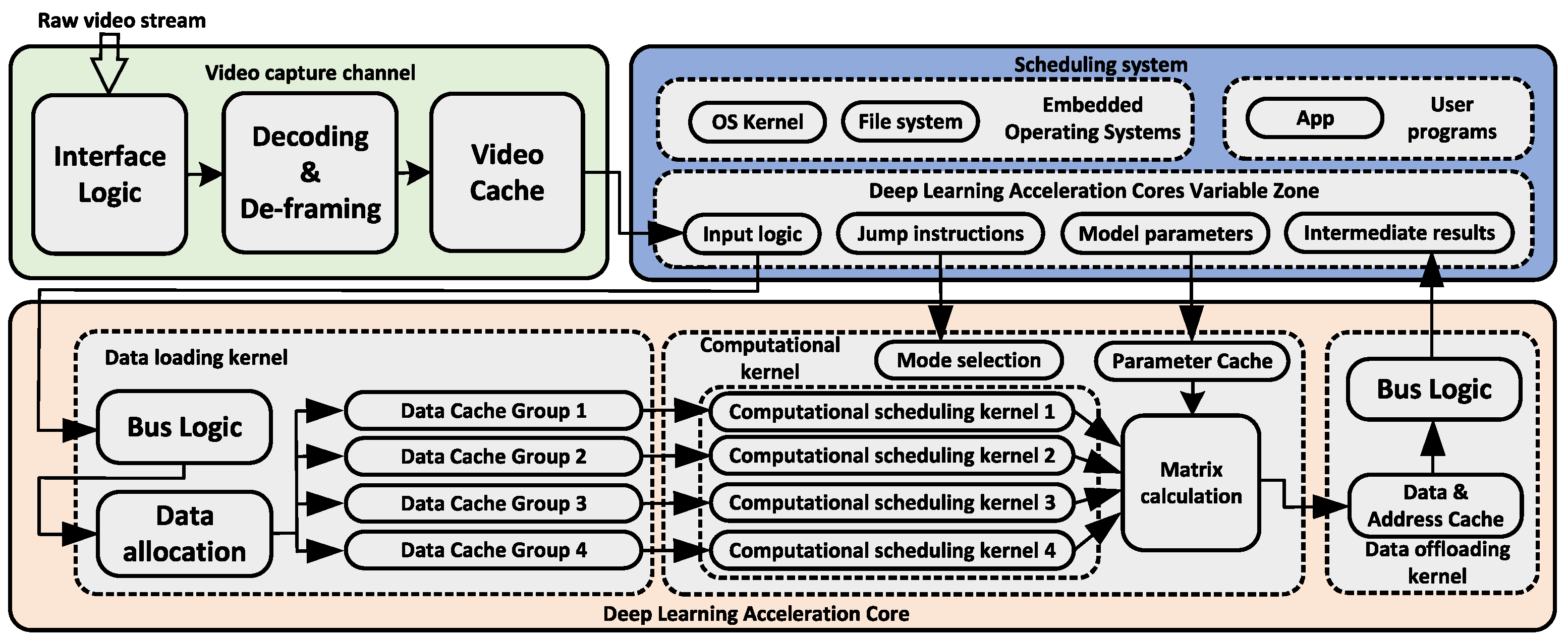
Figure 1. The architecture consists of three parts, the first part is the video capture channel, the second part is the deep learning acceleration core, the third part is the scheduling system.
Applsci 13 04144 g001
Figure 2. A full view of our proposed method.
Applsci 13 04144 g002
Figure 3. The parallel acceleration of the convolution layer is divided into three main dimensions: input channel parallelism, output channel parallelism, and pixel parallelism.
Applsci 13 04144 g003
Figure 4. Input channels are 3. Input parallelism is 8. Output parallelism is 8. Pixel parallelism is 4. Internal data flow diagram of the Computational kernel.
Applsci 13 04144 g004
Figure 5. Pooling layer parallel computing method.
Applsci 13 04144 g005
Figure 6. Computational kernel data remapping.
Applsci 13 04144 g006
Figure 7. Computational kernel input data remapping.
Applsci 13 04144 g007
Figure 8. Top: pipeline constraint effect. Bottom: unroll constraint effect.
Applsci 13 04144 g008
Figure 9. Array_partition constraint effect.
Applsci 13 04144 g009
Figure 10. AXI burst mode timing diagram in read mode.
Applsci 13 04144 g010
Figure 11. AXI outstanding mode timing diagram in read mode.
Applsci 13 04144 g011
Figure 12. Clock domain generation block diagram.
Applsci 13 04144 g012
Figure 13. DSP48E Cross-Clock Domain Design.
Applsci 13 04144 g013
Figure 14. Diagram of clock follower and the output waveform of each point of the clock follower.
Applsci 13 04144 g014
Figure 15. Video processing heterogeneous system board.
Applsci 13 04144 g015
Figure 16. Pipeline experiment results: (a) Convolutional layer pipeline synthesis result. (b) Fully connected layer pipeline synthesis results. (c) Computational scheduling kernel pipeline diagram.
Applsci 13 04144 g016
Figure 17. Overall resource consumption of the hardware platform.
Applsci 13 04144 g017
Figure 18. The actual output of the bridge detection in the aerial video using TinyYolo inference with the acceleration core.
Applsci 13 04144 g018
Table 1. TinyYolo loading strategy for each layer part.
Input Tensor/Output TensorPartial Loading Input Tensor/ Output TensorOccupy the Data Loading Area DepthOccupy Data Storage Area DepthOccupy the Parameter Storage Area Depth
CONV1448 × 448 × 3/
448 × 448 × 16
56 × 56 × 3/
56 × 56 × 16
784627218
POOL2448 × 448 × 16/
224 × 224 × 16
56 × 56 × 16/
28 × 28 × 16
156815680
CONV3224 × 224 × 16/
224 × 224 × 32
28 × 28 × 32/
28 × 28 × 32
784313672
POOL4224 × 224 × 32/
112 × 112 × 32
28 × 28 × 32/
14 × 14 × 32
7847840
CONV5112 × 112 × 32/
112 × 112 × 64
28 × 28 × 32/
28 × 28 × 64
7846272288
POOL6112 × 112 × 64/
56 × 56 × 64
28 × 28 × 64/
14 × 14 × 64
156815680
CONV756 × 56 × 64/
56 × 56 × 128
14 × 14 × 64/
14 × 14 × 128
39231361152
POOL856 × 56 × 128/
28 × 28 × 128
14 × 14 × 128/
7 × 7 × 128
7847840
CONV928 × 28 × 128/
28 × 28 × 256
14 × 14 × 128/
14 × 14 × 64
78415681152
POOL1028 × 28 × 256/
14 × 14 × 256
14 × 14 × 256/
7 × 7 × 256
156815680
CONV1114 × 14 × 256/
14 × 14 × 512
14 × 14 × 256/
14 × 14 × 32
15687841152
POOL1214 × 14 × 512/
7 × 7 × 512
2 × 2 × 512/
1 × 1 × 512
128640
CONV137 × 7 × 512/
7 × 7 × 1024
7 × 7 × 512/
7 × 7 × 16
896981152
CONV147 × 7 × 1024/
7 × 7 × 1024
7 × 7 × 1024/
7 × 7 × 8
1792491152
CONV157 × 7 × 1024/
7 × 7 × 1024
7 × 7 × 1024/
7 × 7 × 8
1792491152
FC171 × 1 × 50,176/
1 × 1 × 256
1 × 1 × 50,176/
1 × 1 × 2
156811568
FC181 × 1 × 256/
1 × 1 × 4096
1 × 1 × 256/
1 × 1 × 512
8642048
FC191 × 1 × 4096/
1 × 1 × 1470
1 × 1 × 4096/
1 × 1 × 32
12842048
Table 2. Computational scheduling kernel resource consumption.
LUTFFDSPBRAM
Computational scheduling kernel as a whole47739333165469.5
Convolutional Computing Pipeline3684725028410
Pooling Computing pipeline2400186490
Fully Connected Computing Pipeline7169475640
ZU15EG on-chip resources3412806825603528744
Computational scheduling kernel Occupancy13.9%4.8%1.5%9.3%
Table 3. Deep learning acceleration core overall resource consumption.
LUTFFDSPBRAM
Computational scheduling kernel47739333165469.5
Data Storage kernel55635868218
Data Loading kernel2619342867.5
Internal Storage73210080
DSP Calculation Matrix4994311391280
Acceleration core overall6163473761209165
Overall Occupancy18.0%10.8%5.9%22.1%
Table 4. TinyYolo parameters for each layer part.
LayerInput TensorOutput TensorNumber of ParametersData VolumeCalculated Volume
Input0 448 × 448 × 3016056320
CONV1448 × 448 × 3448 × 448 × 1611523211264231211008
POOL2448 × 448 × 16224 × 224 × 1608028163211264
CONV3224 × 224 × 16224 × 224 × 3246081605632231211008
POOL4224 × 224 × 32112 × 112 × 3204014081605632
CONV5112 × 112 × 32112 × 112 × 6418432802816231211008
POOL6112 × 112 × 6456 × 56 × 640200704802816
CONV756 × 56 × 6456 × 56 × 12873728401408231211008
POOL856 × 56 × 12828 × 28 × 1280100352401408
CONV928 × 28 × 12828 × 28 × 256294912200704231211008
POOL1028 × 28 × 25614 × 14 × 256050176200704
CONV1114 × 14 × 25614 × 14 × 5121179648100352231211008
POOL1214 × 14 × 5127 × 7 × 512025088100352
CONV137 × 7 × 5127 × 7 × 1024471859250176231211008
CONV147 × 7 × 10247 × 7 × 1024943718250176462422016
CONV157 × 7 × 10247 × 7 × 1024943718250176462422016
FLAT167 × 7 × 10241 × 1 × 50,1760501760
FC171 × 1 × 50,1761 × 1 × 2561284505625612845056
FC181 × 1 × 2561 × 1 × 4096104857640961048576
FC191 × 1 × 40961 × 1 × 1470602112014706021120
Total 4508019296647022569558016
Table 5. Calculation time for convolutional layers.
LayerData Loading TimeData Storage TimeParameter Loading TimeCalculation TimeActual Time
CONV10.67 ms1.33 ms0.00 ms3.01 ms3.01 ms
CONV30.33 ms0.67 ms0.00 ms3.01 ms3.01 ms
CONV50.16 ms0.33 ms0.00 ms3.01 ms3.01 ms
CONV70.08 ms0.16 ms0.03 ms3.01 ms3.14 ms
CONV90.04 ms0.08 ms0.12 ms3.01 ms3.13 ms
CONV110.02 ms0.04 ms0.49 ms3.01 ms3.50 ms
CONV130.01 ms0.02 ms1.96 ms3.01 ms4.97 ms
CONV140.02 ms0.02 ms3.93 ms6.02 ms9.95 ms
CONV150.02 ms0.02 ms3.93 ms6.02 ms9.95 ms
Total1.35 ms2.67 ms10.46 ms33.11 ms43.57 ms
Table 6. Calculation time for fully connected layers.
LayerData Loading TimeData Storage TimeParameter Loading TimeCalculation TimeActual Time
FC170.02 ms0.00 ms5.35 ms1.33 ms6.68 ms
FC180.00 ms0.00 ms0.44 ms0.11 ms0.55 ms
FC190.00 ms0.00 ms2.50 ms0.63 ms3.13 ms
Total0.02 ms0.008.29 ms2.07 ms10.36 ms
Table 7. Comparison of different literature methods.
MethodLiterature [30]Literature [31]Literature [29]Literature [32]Literature [33]Literature [34]Literature [35]This Paper
Hardware PlatformVC707VC707Stratix-V GSD8XC7Z020XC7Z045XC7Z045XC7Z045ZU15EG
Clock frequency100 MHz100 MHz120 MHz214 MHz225 MHz200 MHz125 MHz300 MHz
DSP/Quantity280028001963220576900900209
Performance/GOPS85.261.6272.484.345.13107124153.60
DSP efficiency/
(GOPS/Quantity)0.0300.0220.0370.380.0780.120.140.734
Power7.6 W6.6 W10.4 W3.5 W5.7 W9.6 W4.8 W5.3 W
Energy Efficiency/
(GOPS/W)11.29.3366.9624.087.9111.1425.828.98
ModelKNNLSTMCNNCNNVGG16U-NetVGGTinyYOLO
Disclaimer/Publisher’s Note: The statements, opinions and data contained in all publications are solely those of the individual author(s) and contributor(s) and not of MDPI and/or the editor(s). MDPI and/or the editor(s) disclaim responsibility for any injury to people or property resulting from any ideas, methods, instructions or products referred to in the content.