1. Introduction
The role of the LNA is vital in radio frequency (RF) and microwave (MW) receivers. Its performance directly affects the receiver sensitivity as it is generally the first active element to process the received signal. The main function of the LNA is to perform proper impedance matching with the antenna while providing a noise figure (
NF) as low as possible and sufficiently high gain to attenuate the noise contribution of the upcoming stages. However, usually the LNA consumes most of the power available to provide such high performance, leaving the other components in the system with a small DC power budget [
1]. A feasible solution, as seen in [
1,
2,
3], consists of reducing the supply voltage so that the power budget available for the rest of the components in the receiver is relaxed. By adopting this approach, circuit integration is improved as the LNA can be introduced in a wide range of devices and systems since it can be biased with a very low voltage. Another concern in LNA design is the area needed for the final circuit since conventional LNA design involves the use of bulky inductors to perform impedance matching, source degeneration, inductive neutralization, gain peaking or resonate internal transistor capacitances, among other techniques [
4,
5]. Although the inductor size is reduced as the operating frequency increases, the area use can be further improved if a transformer-based approach is introduced, bringing multiple advantages to the designer as it allows higher gain and bandwidth and lower noise as well [
6].
The differential architecture presents advantages such as a high common mode rejection ratio (CMRR), better ground plane quality, lower parasitic effects of chip interconnections, wider dynamic range and easier coupling between stages, among others. Differential circuits allow direct coupling between stages, avoiding the need for DC isolation capacitors and complex interstage matching networks. As a result, it reduces the area of the integrated circuit and, therefore, its manufacturing costs. Numerous works available in the scientific literature introduce differential LNAs to facilitate system-on-chip integration since they provide high resilience to power supply and common-mode noise [
7,
8,
9,
10]. However, in differential circuits, the number of components and the power consumption are doubled. In addition, the use of a balun (BALanced-to-UNbalanced) is necessary to transform the single-ended (SE) input signal into a differential signal. Integrated transformer design is gaining prominence in mm-Wave circuit design. Several works have been published recently regarding the design and modeling of integrated transformers for various applications [
11,
12,
13]. Nevertheless, this element produces extra losses in the signal path due to the limited values of the magnetic coupling coefficient (
k) and quality factor (
Q) achievable in integrated technologies, which can negatively impact the
NF of the LNA.
In contrast to traditional bulk silicon (Si) complementary metal-oxide-semiconductor (CMOS) processes, SOI technologies present multiple advantages, such as reduction of parasitic capacitances, improvement of device performance and speed, downsizing to nanometer dimensions, reduction of device operating voltage and lower power consumption, among others [
14]. Therefore, the proposed circuit is implemented using an SOI process design kit (PDK) from Global Foundries.
In this work, a fully differential LNA with transformer-based interstage matching networks for K-band applications is presented. The LNA is based on a two-stage CS (common source) topology and is developed in a 45 nm SOI (45RFSOI) process from Global Foundries. The main features of the proposed circuit are a
NF as low as 2.2 dB, a gain of 12.9 dB, input and output return losses (IRL and ORL) above 10 dB, an IIP3 of −4 dBm, and power consumption of 11.7 mW from a 0.38 V DC supply in a very compact area (0.15 mm
2). This is possible thanks to the transformer-based approach, which allows improved area use as they simultaneously act as RF chokes to bias the active devices, and as baluns at the input and output terminals to convert the SE signal into differential mode, and vice versa. To implement the transformers we replicated a state-of-the-art tool into a MATLAB script that generates and equalizes the desired inductances to perform impedance matching for a given frequency and coupling factor value. The content of this paper is organized as follows: the circuit design is discussed in
Section 2, and the implementation of the interstage transformers is discussed in
Section 3. Then, in
Section 4, the simulated S-parameters,
NF, and non-linearity results are shown, along with a comparison with state-of-the-art LNAs. Finally, in
Section 5, the conclusions of this work are drawn.
2. Circuit Design
The main concern in LNA design is the achievement of the lowest
NF possible because it is critical for the overall
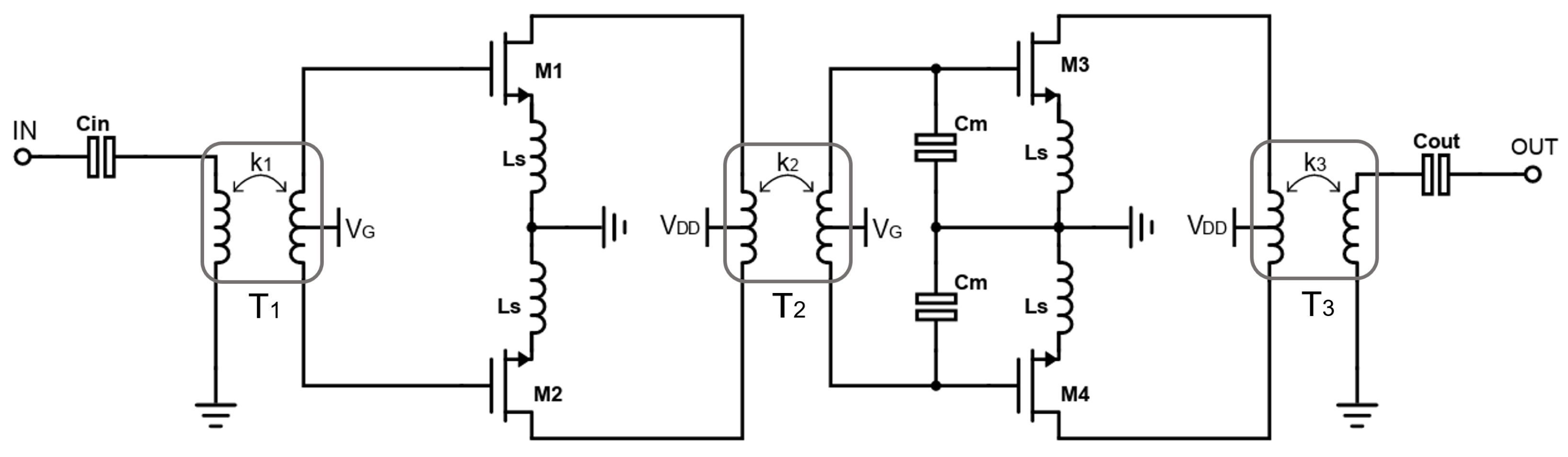
NF of the system. In this work, the LNA is divided into two fully differential CS stages with source degeneration, as shown in
Figure 1. All the values of the passive components used in the circuit are described in
Table 1. The advantage of using a CS topology with inductive degeneration is the possibility of simultaneously achieving impedance matching for minimum
NF and maximum gain (
Gmax) [
15]. This topology is widely used in applications with very low
NF. In comparison to CS amplifiers, the common gate (CG) topology is frequently used in wideband applications, because of its potential to achieve a higher gain. However, the
NF obtained is usually higher in comparison with CS amplifiers. On the other hand, a higher gain can be obtained with a cascode architecture as well, but at the expense of higher power consumption, since the supply voltage cannot be reduced due to the presence of two transistors in the same branch. Transistors M1 and M2 in
Figure 1 are the core of the first stage, and are biased with the DC voltage
VG. Transistors M3 and M4 are the core of the second stage, and they are sized and biased exactly as M1 and M2. The degeneration inductances
Ls are used to improve the noise and IRL of both stages. The input matching network of the circuit is efficiently implemented by the input transformer T1, which is characterized by the coupling factor
k1, primary inductance
Lp1, and secondary inductance
Ls1. The same applies to transformers T2 (
k2,
Lp2,
Ls2) and T3 (
k3,
Lp3,
Ls3). Transformer T1 performs three tasks simultaneously: translation from SE to differential mode, impedance matching, and efficient DC biasing of transistors M1 and M2 through the center tap connection of the secondary. In the same way, transformer T3 has the same task at the output node, but it converts the differential mode signal into SE mode in order to facilitate the measurement procedure of the amplifier. Transformer T2 is used to couple stages 1 and 2 and is also efficiently used to bias the drains of M1 and M2, and the gates of M3 and M4 at the same time, while performing interstage impedance matching. An integrated transformer occupies the same space as a single inductor but performs three tasks simultaneously, therefore, we are able to save a significant amount of area. Finally, capacitors
Cm of 195 fF are used at the gates of M3 and M4 to improve impedance matching without significantly compromising the performance and area of the resulting circuit.
To perform device sizing, we inspect the most relevant performance metrics (i.e., the minimum
NF and
Gmax) in relation to the current density
JDS for a number of device geometries. As depicted in
Figure 2, for a device geometry of 60 μm with 120 fingers (0.5 μm per finger), a minimum
NF of 1.17 dB is obtained when the device is biased with a
JDS of 0.1286 mA/μm. Thus, a drain current
IDS of 0.1286 mA/μm × 60 μm = 7.71 mA is required. To achieve this current density, a gate voltage
VG of 0.38 V is employed. Therefore, we choose this size and biasing conditions for the CS transistors M1 and M2. Once the device is biased with a DC drain current of 7.71 mA, the resulting optimum source impedance
Sopt required at the gate of M1 and M2 is calculated to achieve the minimum
NF. In a conventional design, a complex input matching network would be needed to match the
Sopt to the 50 Ohms of the input antenna, but thanks to the differential approach, we are able to efficiently use transformers for this task.
The Global Foundries 45-nm RFSOI PDK is used to design the layout of the transformers. The design kit offers 7 copper (Cu) layers (M1-M3, C1, UA, OA, OB) and a 4.125-μm thick aluminum (Al) layer. The OB and OA metal layers are used to implement all the inductors since they are composed of copper lines with the same thickness (3 μm), which facilitates the equalization of inductors. That is, it facilitates the obtention of the same inductance and quality factors of the windings of the primary and secondary inductors [
16]. Since the transistors are placed on the substrate and the passive components are generally implemented in the top metal layers to obtain the highest quality factor (
Q) possible, a number of vias and interconnections have to be added to bring the connections of the gate, source, and drain terminals from the low, thin metal layers to the top, thick layers. So as to account for the effect of these metal interconnections on the LNA performance, we developed the layout of the selected transistor early in the design procedure to consider these effects [
17]. The 3D view of the developed layout is presented in
Figure 3a and the front view of the same layout is shown in
Figure 3b. To prepare the layout of the active device, we sliced it down to 4 instances of 15 μm with 30 fingers each, which allows gate, drain, and source interconnections complying with the design kit physical rules, since low metal layers have very restrictive constraints related to their maximum width and area. To minimize parasitic capacitances at the gate, drain, and source nodes we employed a staircase configuration. This implementation also caters to the reduction of the gate resistance and parasitic capacitances to optimize the achievable minimum noise figure (
NFmin) of this device. In this sense, the
NFmin for a MOS device can be expressed as (
1), where
K is a constant value,
gm is the transconductance of the device,
RG is the gate resistance,
RS is the source resistance,
f is the working frequency and
fT is the unity current gain frequency [
4]. Hence, maximizing
fT (by minimizing parasitic capacitances) and minimizing
RG and
RS allows the reduction of
NFmin.
The new, complex model of the FET is composed of the intrinsic PDK FET device, an RC parasitic extraction of the interconnections from M1 to C1 layers using Calibre xRC, and an EM simulation model generated with EMX of the interconnections from UA to OB metal layers.
The design of the 0.38 V low-power LNA is possible thanks to the CS current density design approach, which is detailed as follows. The active device provides an excellent noise performance at JDopt = 0.1286 mA/μm. Hence, the device provides optimal noise performance when it is biased with IDS of 7.71 mA. We can then search for a combination of VD and VG that yields the desired IDS. Since the LNA is formed by two cascaded CS stages, we can reduce the nominal 0.9 V drain DC voltage required by the PDK and increase the gate DC voltage accordingly to maintain the same JDS, which results in a severe reduction in power consumption without significantly compromising the LNA performance. This would not be possible if a cascode topology had been used. The DC supply voltage is reduced from 0.9 V to 0.38 V and the gate voltage VG is increased to 0.38 V as well. With these values, the drain current IDS is 7.71 mA as desired, ensuring minimum NF performance with little deviation in gain and impedance matching of the LNA.
3. Transformers Implementation
A transformer is a passive structure composed of primary and secondary inductors (
Lp and
Ls), with a certain magnetic coupling coefficient
k between them. In a transformer,
k determines the strength of the magnetic coupling between the windings and is given by (
2), where
M is the mutual inductance between the primary and the secondary.
Due to the overlapping, the proximity of the windings, and the dielectric constant of the substrate material, designers have to deal with a finite parasitic capacitance (
Cpar) which can give rise to a low value of the self-resonant frequency (SRF). The SRF is the frequency at which the transformer resonates, determined by (
3), and it limits the range of use of the transformer. This is because
Cpar is proportional to the inductance value (
L). In electronic circuit design, it is desirable for the operating frequency to be a fraction of SRF in order to attain the maximum possible inductance for a given operating frequency. However, as the frequency increases, the utilization of large inductances becomes increasingly challenging due to the corresponding increase in
Cpar with frequency. Since we are dealing with the design of a K-band LNA, the transformers need to be designed to present an SRF in the order of 50 GHz, which is achieved by means of layout techniques.
To size the transformers defining the values of
k,
Lp, and
Ls, the designer must obtain the desired source and load impedances (
ZS and
ZL, respectively). The impedance
ZS refers to the impedance seen at the input terminal of the transformer (the primary), while impedance
ZL is the impedance at the output node of the transformer (the secondary), which is equivalent to the conjugate value of the desired
Sopt. This situation is reflected in
Figure 4.
Instead of using a discrete analytical solution as an approximation to the final values of
k,
Lp, and
Ls, the transformer-based impedance matching tool proposed in [
12] is replicated in MATLAB for transformer sizing and inductance equalization. The developed tool receives the working frequency
f, the magnetic coupling coefficient
k, the source impedance
ZS, and the load impedance
ZL as inputs, and it produces the inductance values of a transformer that matches the given impedances at the operating frequency.
The MATLAB script generates the values of inductances
Lp and
Ls to match the two impedances at the given frequency and magnetic coupling coefficient. In addition, an equalization process is implemented, following [
12], to adjust the inductors to present the same inductance value,
Leq. As a result of the equalization process, an additional passive element has to be added to the source or load of the transformer to perform impedance matching. This is the reason why the capacitors
Cin,
Cm, and
Cout are added to the schematic in
Figure 1.
Due to the nature of integrated technologies, achieving a
k greater than 0.8~0.9 can be challenging. The EMX full-wave electromagnetic (EM) solver has been used to explore the
k values that can be achieved in the 45RFSOI technology (~0.7). The MATLAB tool is then used to calculate the inductances needed to match
ZS with
ZL for this
k value. Obtaining the desired inductances depends on the geometry and physical properties of the metals and layers used, so obtaining them is an iterative process, highly dependent on the physical structure used. The final design of the transformers is shown in
Figure 5. The layout design has been based on the proposal in [
18]. The design of T1 is the most challenging due to its high
Leq value (751 pH), and as the first element in the circuit, it is crucial to minimize its losses. As studied in [
16], there are several ways to design an integrated transformer. One option is a stacked layout, which allows for a high magnetic coupling (
k = 0.6~0.8) but also leads to a large parasitic capacitance between the primary and secondary inductors since they are completely overlapped. In the case of transformer T1, it is designed using a stacked layout with interwound windings to obtain a high SRF. The transformer’s primary and secondary inductors are implemented with two turns, with the secondary being larger in size compared to the primary. However, this inductance difference is compensated by extending the connection of the primary to the ground, which adds a small inductance to compensate for the difference.
For the other two transformers, the goal is to maximize
k and minimize the area at the expense of decreasing the SRF. To achieve this, the primary and secondary metals were stacked. Transformer T2 has only one turn as the required
Leq2 is 312 pH, while the
Leq3 needed in T3 is 475 pH, which is why it was implemented with two turns.
Table 1 shows the values of all the elements used in the design of the LNA.
4. Simulation Results and Comparative
The performance of the proposed LNA was obtained with Spectre RF Simulator after performing the post-layout parasitic extraction in Cadence Virtuoso using Calibre PEX tools. The LNA consumes a DC current of 30.7 mA, resulting in a power consumption of 11.7 mW. The simulation results of the S-parameters are shown in
Figure 6a. A maximum gain of 12.9 dB is obtained at 21.2 GHz, with a 3 dB bandwidth ranging from 20.3 to 24.1 GHz. The ∣
S11∣ and ∣
S22∣ are lower than 10 dB from 20.7 to 21.7 GHz and from 21.4 to 24.6 GHz, respectively. The ∣
S12∣ is less than 19.5 dB over the whole band. The simulated results of
NF and Rollet stability factor (k-Rollet) are shown in
Figure 6b. The
NF has a minimum value at 22.4 GHz and varies between 2.2 and 3.5 dB within the 3 dB bandwidth. Note the amplifier is unconditionally stable as long as the value of k-Rollet is above one. The layout of the proposed LNA is shown in
Figure 7.
The simulation results of the non-linearity analysis are shown in
Figure 6c, concluding that the proposed LNA achieves a P
o1dB of −7.3 dBm, and an OIP3 of 7 dBm. To validate the results, a 250-occurrences Monte Carlo run is performed to determine if the performance meets the specifications under all conditions. The histograms containing the information of this analysis are presented in
Figure 8a–d. As shown, the IRL (
Figure 8a) is better than 8 dB and the ORL (
Figure 8b) is better than 15 dB. The gain and
NF of the LNA are depicted in
Figure 8c,d, respectively, concluding the LNA achieves a gain above 11.5 dB and an
NF of 2.2 dB at 22 GHz.
The performance of the proposed LNA is compared with recent publications in
Table 2, Refs. [
7,
8,
9,
10]. Only differential LNAs are considered. In order to provide a fair comparison with similar works, the figure of merit (
FoM) defined in (
4) is used in the table, where
g is the linear gain of the LNA,
BW is the bandwidth in Hz,
F is the noise factor,
PDC represents the power consumption, and
area is the total circuit area. A similar definition of this (
FoM) can be found in [
10,
15,
19].
The work proposed in [
7] demonstrates the design of a low-phase noise, source degenerated K-band cascode LNA with transformer-based matching networks and current steering to achieve a variable gain. The amplifier obtains a gain of 18.5 dB, with 4.1 dB
NF and a 14.5 dBm OIP3. However, this high-performance circuit results in significant power consumption (67.2 mW from a 1.2 V DC power supply), which is reflected in the low value of the
FoM (1.71). In [
8], the authors present a variable gain LNA as well, employing a split-common gate transistor technique in a two-stage cascode LNA. The authors report a very high gain of 25 dB and a low
NF (3.4 dB) at 22 GHz, drawing 25.2 mW from a 1.2 V DC supply. Nevertheless, the LNA operates in a narrow bandwidth of 2 GHz. A very compact (0.11 mm
2) 45 nm RFSOI 28-GHz LNA is introduced in [
9], based on a source degenerated cascode with integrated baluns. The circuit achieves a gain of 9 dB, a
NF of 3.1 dB, and very high linearity (IIP3 = 10 dBm), over a bandwidth of 4.5 GHz, with a total power consumption of 34 mW from a 1.8 V DC power supply. This performance trade-off results in a significant improvement of the
FoM (9.63). Another 45 nm RFSOI LNA is introduced in [
10], based on a 3-stage cascode amplifier with baluns and switched capacitors to achieve multiband operation. The LNA presents a gain of 19.5 dB, a
NF of 4.7 dB, but at the expense of a total power consumption of 59 mW and an area of 0.32 mm
2, thus lowering the value of the
FoM obtained with this solution.
As shown in
Table 2, the proposed LNA achieves the highest
FoM value (14.5) of all the solutions considered, since circuit performance is a result of an excellent trade-off between the gain,
BW,
NF,
PDC and area. Note that the gain of other contributions is higher at the expense of a significant increase in power consumption. The developed LNA presents the lowest power consumption and
NF reported in a differential LNA, to the best of the authors’ knowledge. In fact, the power consumption in this work is less than half the one used in [
8], which reports the lowest power consumption and highest gain of all the state-of-the-art solutions considered. In addition, we reported a very low
NF, high gain, and high bandwidth in a very compact area.
5. Discussion
A fully differential LNA with transformer-based interstage matching networks for the K band in a 45 nm SOI process is presented. The methodology addresses the improvement of critical design trade-offs, allowing the design of a high-performance, low-power, and very compact LNA. This is accomplished thanks to the transformer-based matching network approach, which allows improved area use, as the transformers simultaneously act as RF chokes and as baluns at the input and output terminals to convert the SE signal into differential mode, and vice versa. In order to generate and equalize the desired transformer inductances a state-of-the-art tool was used following the proposal in [
12]. In addition, a low-power LNA based on optimal current density selection is obtained, allowing the reduction of the nominal DC power supply from 0.9 V to 0.38 V, which results in a significant reduction in power consumption (which is more than halved). The circuit consumes a total power of 11.7 mW from a 0.38 V DC supply, and occupies an area of 0.15 mm
2 excluding pads. The LNA obtains a gain of 12.9 dB, a
NF of 2.2 dB with an IRL higher than 10 dB. Non-linearity simulations show the proposed circuit achieves a P
o1dB of −7.3 dBm, and an OIP3 of 7 dBm. To validate the circuit, EM simulations, and Monte Carlo analysis results are presented as well. Compared to similar works available in the scientific literature, the results of the developed circuit achieve an excellent trade-off between gain, bandwidth, NF, power consumption, and area. In particular, the circuit presents a remarkably low power consumption and NF, obtaining the lowest values reported in a differential LNA compared to the state-of-the-art solutions. Although the reported results of our study demonstrate excellent performance there is room for further improvement. In this sense, future lines of work include the fabrication and measurement of the proposed circuit to validate the results, optimization of the second stage amplifier to improve gain and linearity, integration of the proposed LNA in a complete receiver or a real system, and improvement of the circuit PVT (Process–Voltage–Temperature) resilience.


 ,
, 


