Article

Full Antiferroelectric Performance and GMR Effect in Multiferroic La0.75Ba0.25Fe12O19 Ceramic

State Key Laboratory of Advanced Technology for Materials Synthesis and Processing, Wuhan University of Technology, Wuhan 430070, China
*
Author to whom correspondence should be addressed.
Appl. Sci. 2023, 13(9), 5718; https://doi.org/10.3390/app13095718
Submission received: 7 April 2023 / Revised: 2 May 2023 / Accepted: 3 May 2023 / Published: 5 May 2023

Abstract

:
The potential application of multiferroic materials in new electronic devices attracts more and more attention from people either in an academic field or industry. This paper reports that M-type lanthanum-doped barium ferrite (La0.75Ba0.25Fe12O19) demonstrates full antiferroelectric (AFE) and excellent magnetoelectric coupling effects at room temperature, while its AFE phase displays a zero macroscopic net polarization. The dramatic change in the dielectric constant near the Curie temperature far below room temperature represents the transition from ferroelectrics (FE) to antiferroelectrics. The fully separated double electric polarization hysteresis (P–E) loops confirmed its AFE performance. Its EF and EA are located at 1100 kV/cm and 850 kV/cm, respectively. The large M–H loop showed a strong magnetic property simultaneously. The UV-Vis-NIR optical spectrum revealed that La0.75Ba0.25Fe12O19 is also a semiconductor, whose direct bandgap energy (Eg) was determined to be 1.753 eV. Meanwhile, La0.75Ba0.25Fe12O19 showed strong ME coupling and a GMR effect. A 1.1 T magnetic field reduced its resistance by 110% at 30 kHz. The multiple functions combined in one phase would create new options for high energy storage capacitors, microactuators, pyroelectric safety sensors, cooling devices, and pulsed power generators and so on, as well as great opportunities for generating new electronic devices with active magnetoelectric coupling effects.

1. Introduction

Today, human beings have entered the era of big data, which is generated not only by industry but also by society. The storage and readout of those big data or information consumes huge quantities of energy and greatly improves the temperature of the storage medium and its surrounding environment, due to the induced magnetic field generated by alternating current in traditional information storage and sensors [1]. The resulting large amount of energy consumption generates a large amount of useless heat energy. Therefore, the demand for saving huge quantities of energy for big data storage and reducing the medium’s temperature becomes imperative. However, from this point of view, it has significance for research on low-energy memory and logic devices, in which the field of spintronics focuses on establishing magnetization control without the need for a magnetic field [2], so that the induced magnetic field can no longer be directly generated, thus enabling the device to have the advantages of being faster, smaller, and ultra-low power consuming [3,4]. Upon this demand, multiferroic materials come into the vision of scientists. As the term suggests, multiferroic materials refer to ones with a variety of ferrous properties, such as ferroelectricity (antiferroelectricity), ferromagnetism (antiferromagnetic, ferrimagnetism), and ferroelasticity [5]. Multiferroic materials have gained so much attention because of their unique magnetoelectric coupling effect. Through magnetoelectric coupling, the magnetic state of the material can be changed under an electric field, thereby reducing the energy consumption, volume, and reaction speed of the device [6,7,8,9,10]. It could be predicted that complex structures combining multiferroics with semiconducting and/or spintronics [11,12,13,14] could in the future replace the existing semiconductor-based random access memory and computing technologies [15], leading to a revolution in information storage and computing technology. Recent studies have shown that the dielectric and piezoelectric parameters are greatly improved at room temperature with an increase in grain size. The Curie transition temperature is found to shift slightly towards higher temperatures as the grain increases from 86 nm to 123 nm. The coercive field decreases and the remnant polarization and spontaneous polarization increase as the grain size of BST (Ba0.8Sr0.2TiO3) nanoceramics increases [16,17]. On the contrary, the diffusion degree of the Curie peak increases with the decrease in grain size [18]. The coherent shift in the magnetic ordering and the dielectric anomalies to high temperature with increasing grain size is related to the suppression of the in-plane lattice parameter [19]. The ME coupling was influenced by the interfacial coupling and the density of the phases. Although it was possible to control the process of interdiffusion, a low density caused by differences in thermal expansion reduced the ME coupling. Consequently, it was concluded that ME coupling could be enhanced by the optimization of the interfacial properties [20,21].
BiFeO3 and TbMnO3, the representative candidates of the revival of multiferroic materials, have always been the most-studied [22,23]. However, the weak magnetoelectric coupling and low Curie temperature may limit their application prospective. M-type hexagonal ferrite, on the other hand, has been reported to be multiferroic and show a larger room temperature magnetoelectric coupling effect than other compounds [24,25,26,27,28]. M-type hexagonal ferrite is a traditional ferrimagnetism material and has been widely used in the development of magneto-dielectric devices and fabrication techniques at very low costs [29,30]. A recent study revealed a fully saturated electric polarization (P–E) hysteresis loop in BaFe12O19 ceramics by reduced oxygen vacancies through annealing in a pure oxygen atmosphere, and thus successfully verified the ferroelectrics of BaFe12O19 at room temperature [28]. Traditionally, BaFe12O19 was proved to have excellent magnetic properties [31,32,33]. The magnetoelectric coupling strength of M-type hexagonal ferrites can be further improved by doping with rare earth elements [24,34,35]. Thus, M-type hexagonal ferrites and their doped counterparts may become candidates that can be capable of reaching the milestone of multiferroics [28].
The history of AFE is very short compared to that of FE. Until now, only a few antiferroelectric materials have been discovered, such as PbZrO3, PbHfO3, and NaNbO3 [36,37]. Moreover, the AFE part in the double P–E loops of these AFE phases does not perfectly match the definition of an AFE feature, which should have zero net macroscopic polarization in the AFE region of double P–E loops [38]. It is of great significance to expand the types of new AFE materials and to find perfect AFE features that show zero net macroscopic polarization at room temperature. In the temperature-dependent dielectric constant spectrum of BaFe12O19 ceramics, it was found that the FE–AFE transition occurs at 194 °C [28]. However, it was reported that in PLZ ((Pb1–3/2x Lax)ZrO3) thin films, the appropriate La content can stabilize the AFE phase of PbZrO3 [39]. Meanwhile, Bharadwaja et al. reported that a PLZ AFE film may contain a maximum La content of 9 mol%, and found that adding 1 mol% La reduced the Curie point by about 22 °C [40,41,42]. Therefore, we decided to dope BaFe12O19 with lanthanum, aiming to reduce the Curie temperature of BaFe12O19 down to the low temperature region, thereby realizing the FE–AFE transition at low temperatures and thus achieving a pure AFE phase at room temperature in an LBFO (LaBaFe12O19) system. In this way, we were able to expand the multiferroics to a new type of candidate, which combines both antiferroelectrics (AFEs) and ferromagnetism (FM), in addition to the traditional multiferroics showing the combination of FE + FM or FE + AFM.

2. Material and Methods

In order to precisely control the atomic ratio of the designed compound, we prepared the La0.75Ba0.25Fe12O19 powders by the chemical co-precipitation method with polymer precursors. In this study, Lanthanum acetate (0.4429 g, 0.001307 mol) and Barium acetate (0.1113 g, 0.000436 mol) were dissolved in 20 mL glycerin to form the La + Ba precursor solution. The ferric acetylacetonate (6 g, 0.016989 mol) was dissolved in a mixture solution of 70 mL Aceton and 50 mL ethanol to form an Fe precursor in a 250 mL three neck flask. The La + Ba precursor was poured into the flask to mix with the iron precursor. Then 45 mL of ammonia was added into the flask to co-precipitate the La + Ba and Fe ions. The precipitate paste was separated from the solution by a centrifuge and then calcined at 450 °C and 800 °C, respectively. After a series of steps, Lathan-doped M-type barium hexagonal ferrite (La0.75Ba0.25Fe12O19) powders being composed of 0.75 lanthanum and 0.25 barium was prepared. In this designed compound, 75% Ba was replaced by 75% La from BaFe12O19. Powders of 0.06 g were poured into a Φ6.24 mm round mold and held at a pressure of 1000 msi for 30 s to form a pellet, which was sintered in air at 1400 °C for 3 h into ceramics. However, the ceramic samples made in this way had a large number of oxygen vacancies that were formed during the sintering process; meanwhile, the Fe ions may not have been able to be fully oxidized into Fe3+, instead becoming Fe2+. Either oxygen vacancies or Fe3+/Fe2+ ions may cause current leakage during the P–E measurements, and thus would generate unsaturated or banana-shaped P–E loops. Therefore, it was necessary to perform oxygen annealing for the ceramic samples after sintering in a sealed furnace. The specific operation process was to anneal the ceramic samples in a pure oxygen atmosphere at 800 °C for 6 h, then turn it over to be upside down and perform the same oxygen heat treatment at 800 °C for 6 h. The specimen was finally annealed at 750 °C in a pure oxygen atmosphere for 3 h once more. Both sides of the ceramic samples were coated with a silver paste, which was solidified at 820 °C for 30 min to form silver electrodes.
A structural analysis of the La0.75Ba0.25Fe12O19 powder and bulk ceramic samples was performed using X-ray diffraction (XRD). The morphology of the ceramic surfaces was checked by scanning electron microscopy (SEM). The P–E hysteresis loops were measured on a Sawyer–Tower-circuit-based ferroelectric measurement system. Temperature-dependent dielectric spectra were measured by a Microtest PRECISION 6630 LCR meter. Magnetic properties were measured by a Vibrating Sample Magnetometer (VSM). Lambda 750 S UV-vis-near infrared spectroscopy was used to measure the optical absorption spectrum in the wavelength range of 200–2500 nm. The polarization performance, magneto-dielectric (MD) response, and magnetoelectric coupling (ME) were recorded using a Microtest PRECISION 6300 LCR meter by applying a variable DC magnetic field over a frequency range of 10 Hz to 10 MHz.

3. Results and Discussion

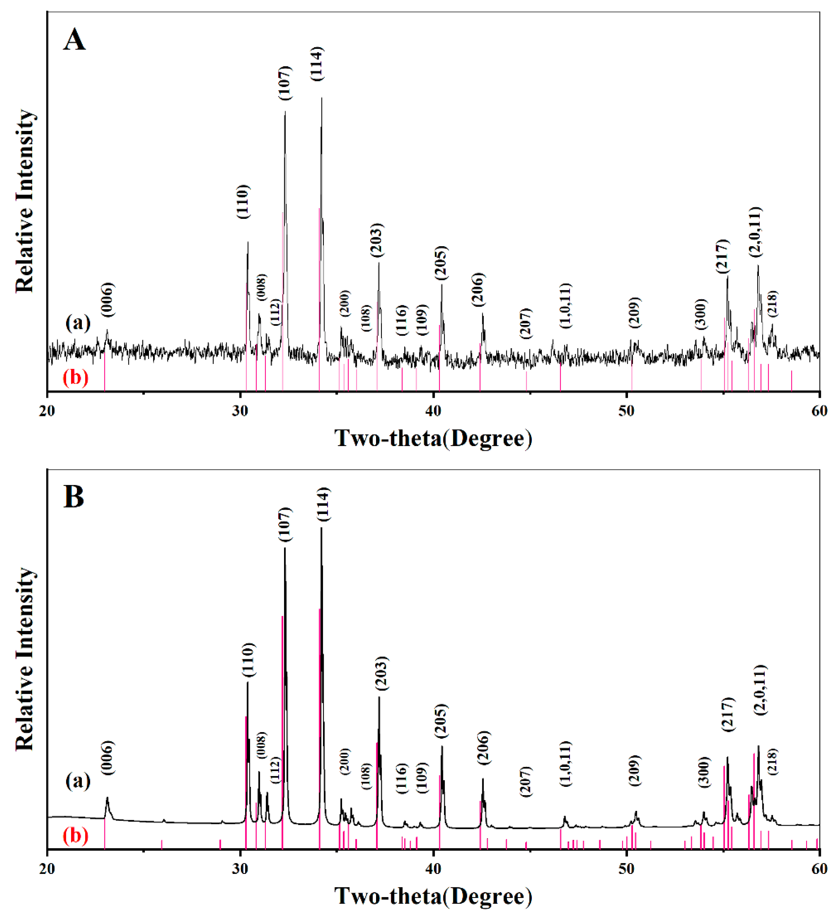
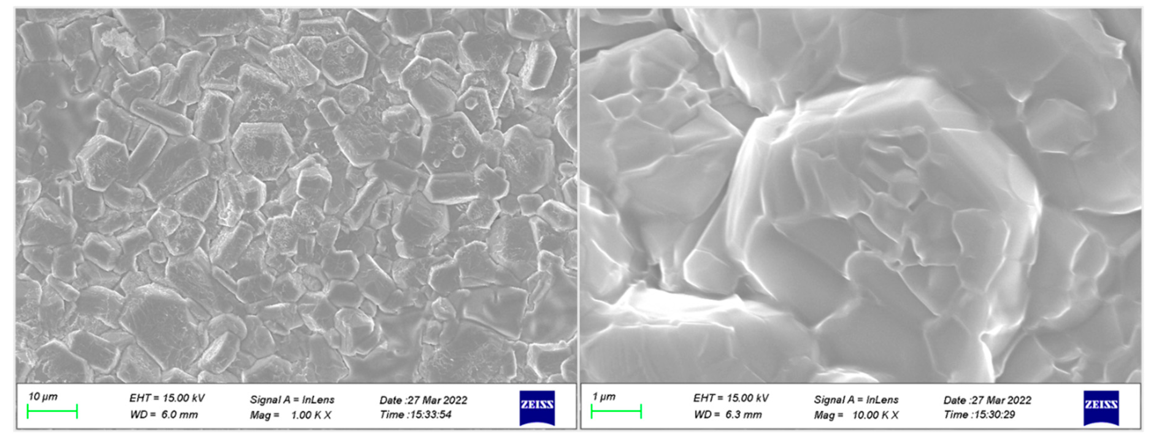
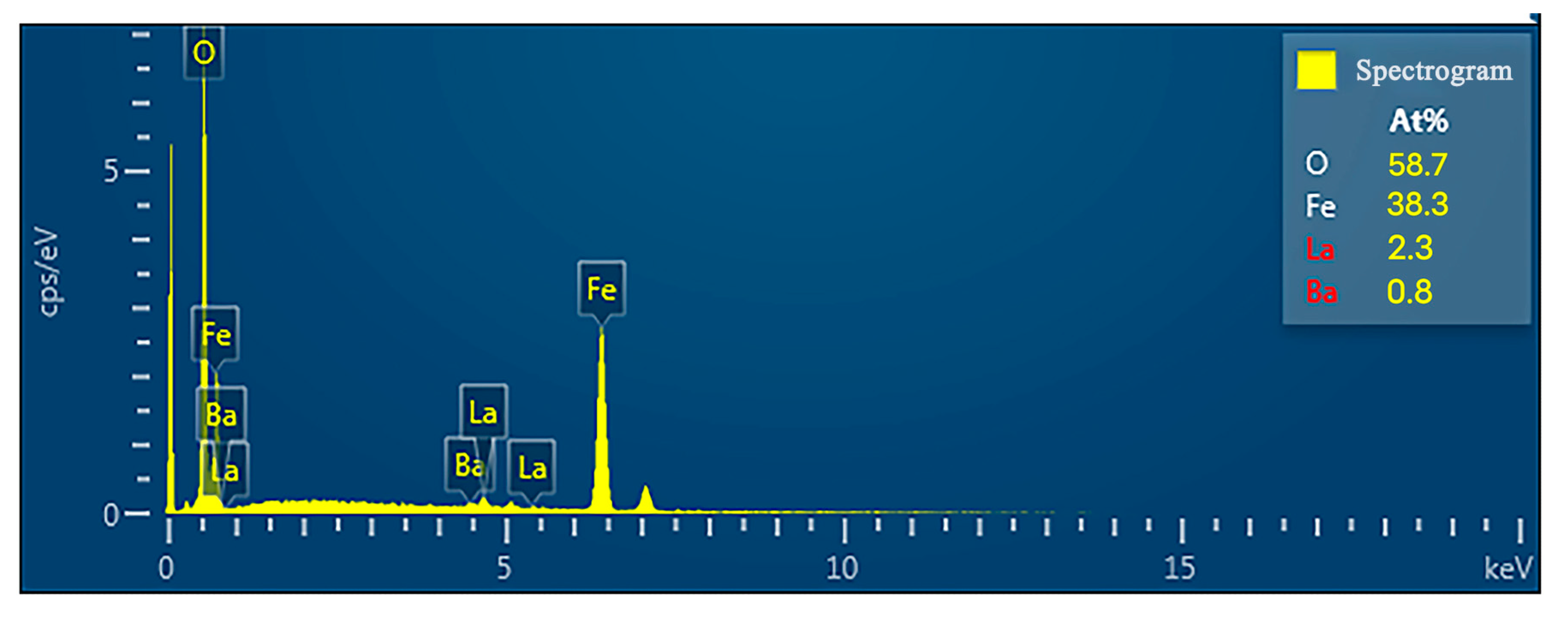
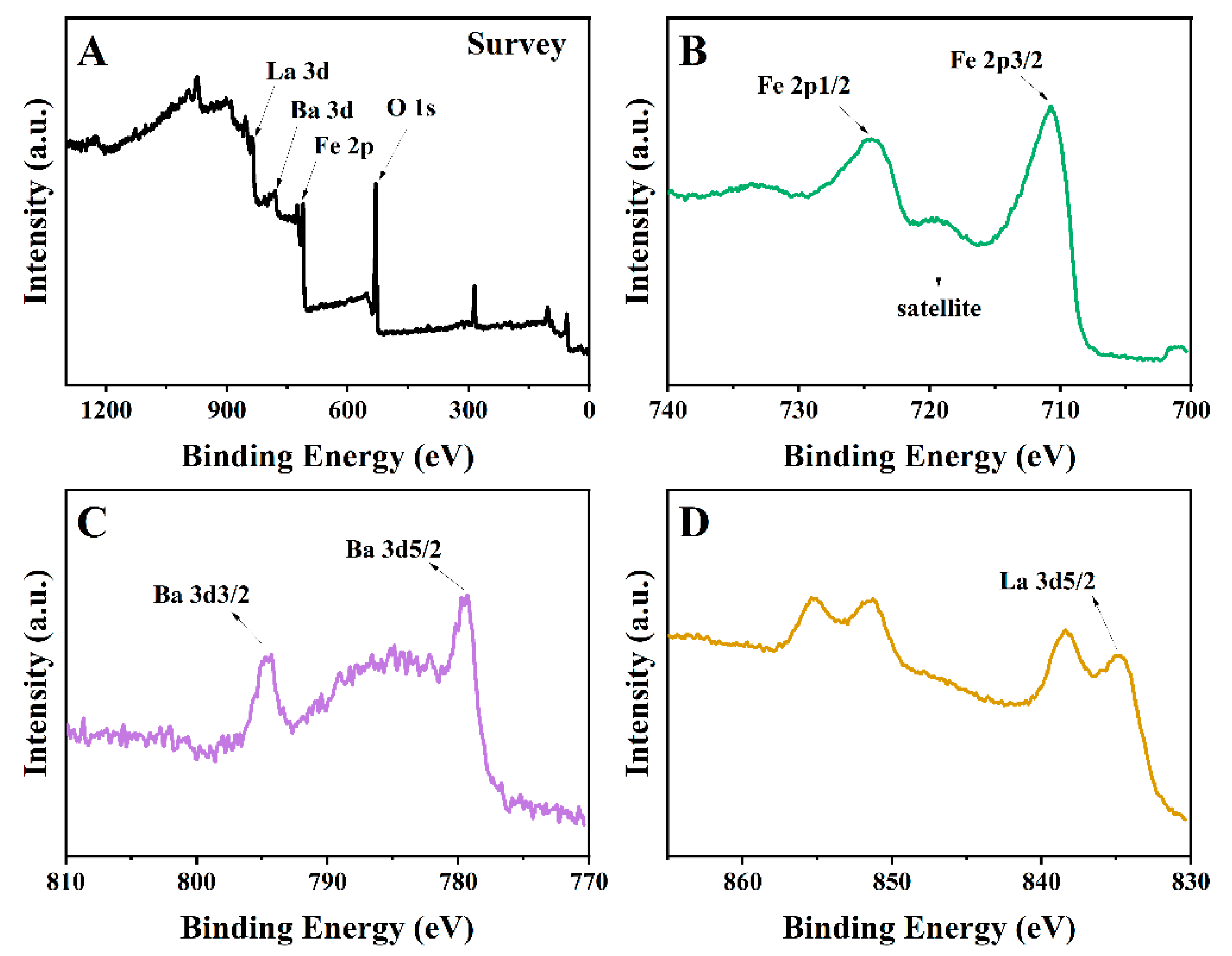
3.1. Structure Identification

In order to verify whether lanthanum successfully entered the crystal lattice of BaFe12O19, replacing part of the barium, the powders’ structure was identified by X-ray diffraction spectroscopy. Figure 1A shows the X-ray diffraction (XRD) spectrum of the as-prepared La0.75Ba0.25Fe12O19 powders, the discrete red lines corresponding to the standard diffraction pattern of BaFe12O19 (PDF#84-0757). It can be seen from Figure 1A that all the diffraction peaks of the sample were in good agreement with the diffraction peaks of the standard card, and no oxides and other ferrite impurities were observed. The XRD data were systematically analyzed using Rietveld refinement, as shown in Figure 1B. Rietveld refinement could fit the XRD profiles well, with a weighted profile R-factor (Rwt) of 4.408% and a GOF factor of 1.19 during the fit, which are at suitable standard levels. The lattice of La0.75Ba0.25Fe12O19 parameters (a) and (c) of 5.8783 and 23.076 Å, respectively, showed some contraction compared to BaFe12O19, and in the XRD diffraction pattern showed a shift in the diffraction peak to the right. This was due to the fact that the atomic radius of lanthanum is smaller than that of barium, so the substitution of lanthanum with barium led to a contraction of the lattice, which was reflected in the XRD pattern as a shift in the diffraction peak to the right. Therefore, it was certain that lanthanum had successfully replaced part of the barium and successfully made pure La0.75Ba0.25Fe12O19 powders in a single magnetoplumbite-5H phase.
Figure 2 shows the morphology feature of the La0.75Ba0.25Fe12O19 ceramic specimen sintered at 1400 °C as measured by scanning electron microscopy (SEM). The results showed that most of the grains were long and flaky when sintered at 1400 °C. It can be seen from Figure 2 that most of the crystal grains of La0.75Ba0.25Fe12O19 were irregular hexagonal plate-like structures, after the substitution of lanthanum with barium, which led to the destruction of the hexagonal symmetry in the crystal lattice of BaFe12O19. The [0001] orientation was parallel to the hexagonal edges of the grains. Since the grains were irregular plate-like structures, this indicated that the grains did not preferentially grow along the [0001] direction, but grew preferentially along the [0100] direction. The grain sizes in the SEM images were counted by Nano Measurer software. The average grain size of La0.75Ba0.25Fe12O19 was 8.44 μm long, 6.50 μm wide, and 4.04 μm thick. The chemical composition of the sintered La0.75Ba0.25Fe12O19 ceramic samples was examined by Bruker scanning electron microscopy (SEM) and energy spectroscopy (EDS). The EDS spectra are shown in Figure 3, and it can be seen that all the elemental lines appear in the spectra. In addition, the atomic ratios are shown in the figure, which can be seen to be basically consistent with those of La0.75Ba0.25Fe12O19. It can be further confirmed that La0.75Ba0.25Fe12O19 was successfully prepared.
It can be proved by previous studies that La0.75Ba0.25Fe12O19 has been successfully prepared. However, there are still some doubts about the valence state of the Fe atoms in it. For this reason, XPS tests were performed on La0.75Ba0.25Fe12O19. The test results are shown in Figure 4, where Figure 4A is the survey spectrum, from which the presence of each element of La0.75Ba0.25Fe12O19 can be seen. Figure 4B is a fine graph of Fe 2p orbitals. From this figure, the binding energies of electrons in Fe 2p3/2 and 2p3/2 orbitals are 710.67 eV and 723.98 eV, respectively. By comparing these with the binding energies of electrons in 2p3/2 and 2p3/2 orbitals of Fe3+ and Fe2+ in the previous literature, it was concluded that Fe was coexisting in La0.75Ba0.25Fe12O19 as 2+ and 3+ [43]. However, the binding energy of Fe2p3/2 in La0.75Ba0.25Fe12O19 was closer to that of Fe3+. Moreover, the distance of 2p3/2 from the satellite peak was 8.01 eV, which is closer to the 9 eV of Fe3+, while it is farther from the 6 eV of Fe2+ [44]. From these two phenomena, it can be concluded that more Fe in La0.75Ba0.25Fe12O19 was present as 3+, where the presence of Fe2+ was due to the substitution of La and insufficient oxygen treatment. The comparison of Figure 4C,D with previous literature on La 3d and Ba 3d can yield evidence for the presence of La and Ba in the tested samples [45,46].

3.2. Antiferroelectricity of La0.75Ba0.25Fe12O19 Ceramics

The P–E hysteresis loop was measured on a ferroelectric measurement system based on the Sawyer–Tower circuit. The measurement results are shown in the Figure 5. It can be clearly identified that La0.75Ba0.25Fe12O19 had obvious AFE characteristics in the fully separated double P–E loops. It can be seen from Figure 5 that its critical forward phase field EF was about 1100 kV/cm, and its critical backward phase field EA was about 850 kV/cm. When the external electric field strength was greater than EF, La0.75Ba0.25Fe12O19 would change from the AFE phase to FE phase due to an electric-field-induced phase transition. Then, when the external electric field was less than EA, the FE phase would transform back to the AFE phase, resulting in a double hysteresis loop.
When the external electric field is small, the adjacent dipoles inside La0.75Ba0.25Fe12O19 are arranged in reverse order and are in an anti-parallel plane state, thus showing zero macroscopic polarization in the P–E diagram. When the external electric field is greater than the EF, the poles in the adjacent dipoles opposite to the external electric field cannot maintain the status due to the enhancement of the electric field, and turn to the same direction as the electric field, thus showing a double hysteresis loop in the P–E diagram. Figure 5 thus fits the definition of AFE very well.
In a previously published paper, it was demonstrated that BaFe12O19 is distinctly FE at room temperature and undergoes an FE–AFE transition at a frequency of 100 Hz and a temperature of 194 °C [28]. While Viehland et al. reported extensive work on PLZT x/95/5 ceramics [47,48,49], and concluded that La doping destroys the long-range dipole order of the FE phase, thereby suppressing the FE phase and stabilizing the AFE phase. Therefore, it is reasonable to suggest that doping La into BaFe12O19 can weaken the FE phase in BaFe12O19, while the opposite AFE phase is gradually stabilized, as it did in PLZT.
Figure 6 shows the recoverable energy density of La0.75Ba0.25Fe12O19 ceramics under different electric fields. It can be seen from Figure 6 that when the electric field was less than 850 kV/cm, it stored almost no energy, and when the electric field was 850–920 kV/cm, its energy storage density increased dramatically. At field range of 920–1100 kV/cm, the energy storage density still increased but the increasing trend began to weaken. At around 1100 kV/cm, its recoverable energy density was the highest, which was 15.31 J/cm3. This phenomenon can be explained as follows. When the electric field goes into the AFE region, the macroscopic polarization is close to zero, which makes it almost impossible to store energy. However, the electric field induces it to transform from the AFE phase to the FE one at EA, where its macroscopic polarization increases rapidly, and the energy storage density increases accordingly. Finally, when the electric field increases to a certain level, the internal AFE phase has been completely transformed into the FE phase, and the energy storage density reaches the highest value in this region. The inset is the measured double electrical polarization loop for a different sample, which is also the data source for the energy storage density map. Thus, it can be shown that the AFE feature of La0.75Ba0.25Fe12O19 is repeatable and reliable.

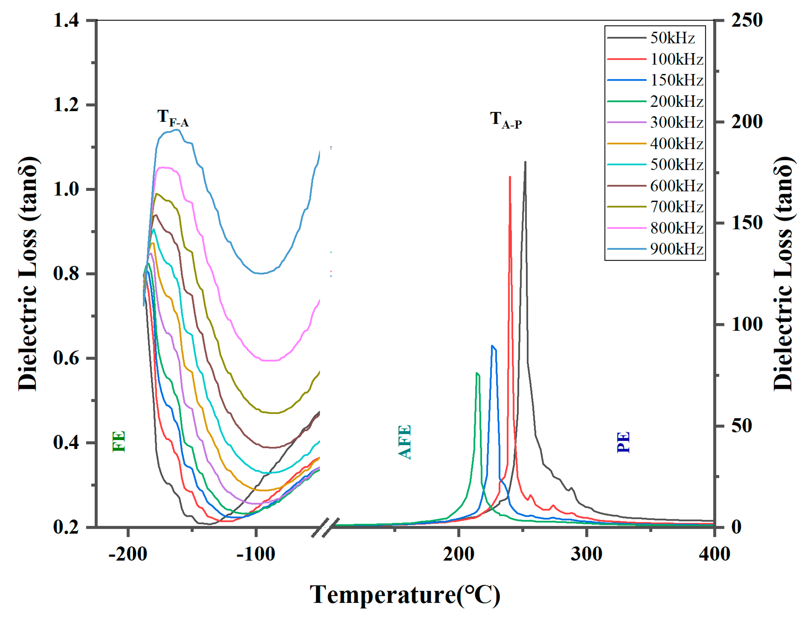
3.3. Dielectric Relaxation Behavior of La0.75Ba0.25Fe12O19 Ceramics

Figure 7 depicts the temperature-dependent dielectric loss spectrum of La0.75Ba0.25Fe12O19 ceramics within a wide temperature range from −200 °C to 400 °C. The frequency spans from 50 kHz to 900 kHz in the low temperature region while it changes from 50 kHz to 200 kHz in the high temperature region. It can be seen from Figure 7 that there appear dielectric anomalous peaks in both the low temperature and high temperature regions, suggesting that La0.75Ba0.25Fe12O19 ceramic undergoes two phase transitions in both the low and high temperature regions.
For the dielectric anomaly peaks at low temperatures, it can be clearly seen that the dielectric anomaly peak shifted to the higher temperature side with increasing frequency, showing a dielectric relaxation behavior. These anomalous peaks were corresponding to the phase transition from ferroelectric (FE) to antiferroelectric (AFE). In this FE–AFE phase transition, when the frequency lifted, the switch duration of the electric field was shortened, and the relaxation time corresponding to it should have also been reduced accordingly. Therefore, the temperature region of relaxation polarization appeared, and the temperature of the dielectric loss peak also increased accordingly. Therefore, the dielectric relaxation behavior in the low temperature part was consistent with the FE–AFE phase transition process. On the other hand, the dielectric anomaly peak in the high temperature region was located within the range of 200–250 °C, above which the AFE phase changed to the paraelectric phase (PE).
La0.75Ba0.25Fe12O19 behaved as an antiferroelectric, while BaFe12O19 behaved ferroelectric at room temperature (RT). The FE–AFE transition temperature and AFE–PE transition temperature of La0.75Ba0.25Fe12O19 were shifted to lower temperatures by about 400 °C and 200 °C, respectively, compared with the FE–AFE and AFE–PE transition temperatures of BaFe12O19 in previous studies [28]. Thus, it can be seen that the doping of lanthanum has an important effect on the FE–AFE and AFE–PE transitions of BaFe12O19, as the doping could switch it from FE to AFE at RT.

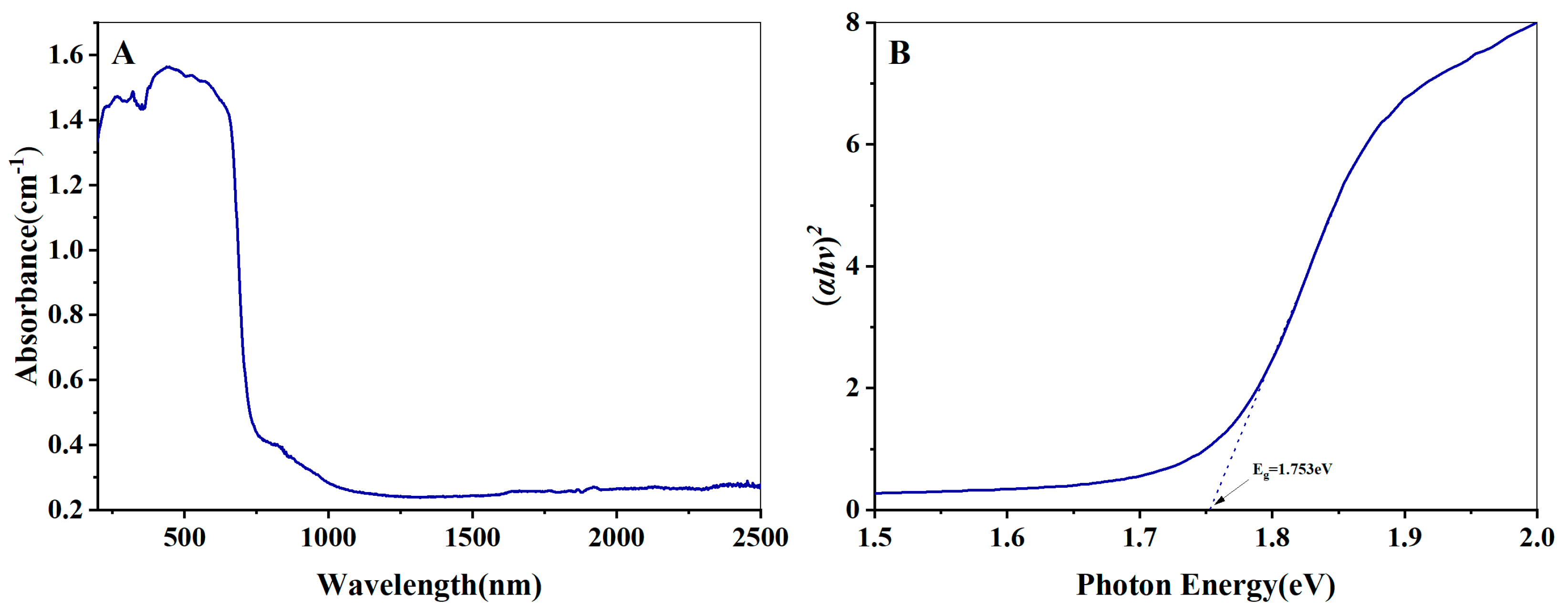
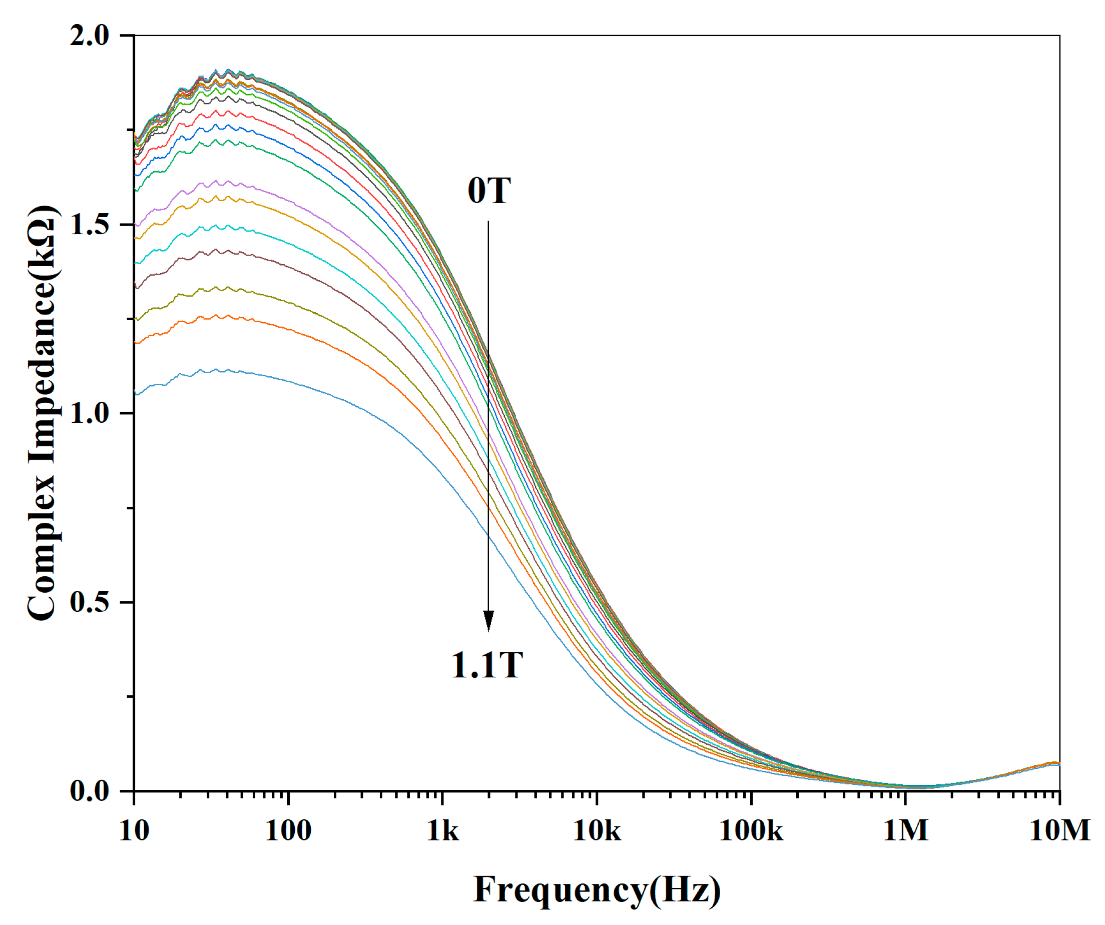
3.4. Magnetic Semiconducting Performance of La0.75Ba0.25Fe12O19 Ceramics

UV-vis optical spectrum is usually used to identify the semiconducting performance of solid materials. A Lambda 750 UV-Vis-NIR spectrometer was used to measure the UV-vis-NIR absorption spectrum of the solid La0.75Ba0.25Fe12O19 ceramics. Figure 8A shows the UV-VIS-NIR absorption spectrum of the La0.75Ba0.25Fe12O19 ceramic specimen measured by this instrument. It can be seen that the absorption coefficient increased sharply within the wavelength range of 750 to 600 nm, reflecting the direct electron transition process from the valence band to conduction band. One stair step with a sharp change in the absorbance indicated that La0.75Ba0.25Fe12O19 is a direct bandgap semiconductor.
The Tauc plot was used to fit the absorption spectrum so as to obtain the forbidden band width of the semiconducting La0.75Ba0.25Fe12O19 compound. The method is based on the formula proposed by Tauc, Davis, and Mott et al., which is as expressed as follows:
α h v 1 n = A h v E g
where α is the absorption coefficient, h is Planck’s constant, v is the frequency, A is a constant, and E g is the semiconductor band gap. When the semiconductor is a direct bandgap semiconductor, n   = 1/2. After processing the absorption spectrum data according to this formula, the data were plotted with α h v 1 n as the y-axis and h v as the x-axis. By linearly fitting the high-slope straight line segment in the figure and extending the fitted line to intersect the x-axis, the intersection is then determined to be the forbidden band width (band gap energy) of the La0.75Ba0.25Fe12O19 semiconductor. The final calculation result is shown in Figure 8B. In this way, the forbidden band width or the band gap energy of the La0.75Ba0.25Fe12O19 ceramic was experimentally determined to be 1.753 eV.
For the magnetic measurement, the La0.75Ba0.25Fe12O19 powder was annealed by oxygen treatment for a total of 15 h in three steps. The magnetization strength M was then measured by a Vibrating Sample Magnetometer (VSM) in relation to the magnetic field strength H. The measurement results are shown in Figure 9, exhibiting a standard M–H hysteresis loop, indicating that La0.75Ba0.25Fe12O19 has a strong ferrimagnetic property. Upon the loop, the saturation magnetization M S was estimated to be 56.402 emu/g, the remnant magnetization M r   was 23.593 emu/g, while the coercivity force H C was 1063.9 Oe.
This combination of ferrimagnetism and antiferroelectrics coexisting in one single phase suggests that La0.75Ba0.25Fe12O19 is a novel type of multiferroic candidate, exhibiting multiple functional responses to external excitation.

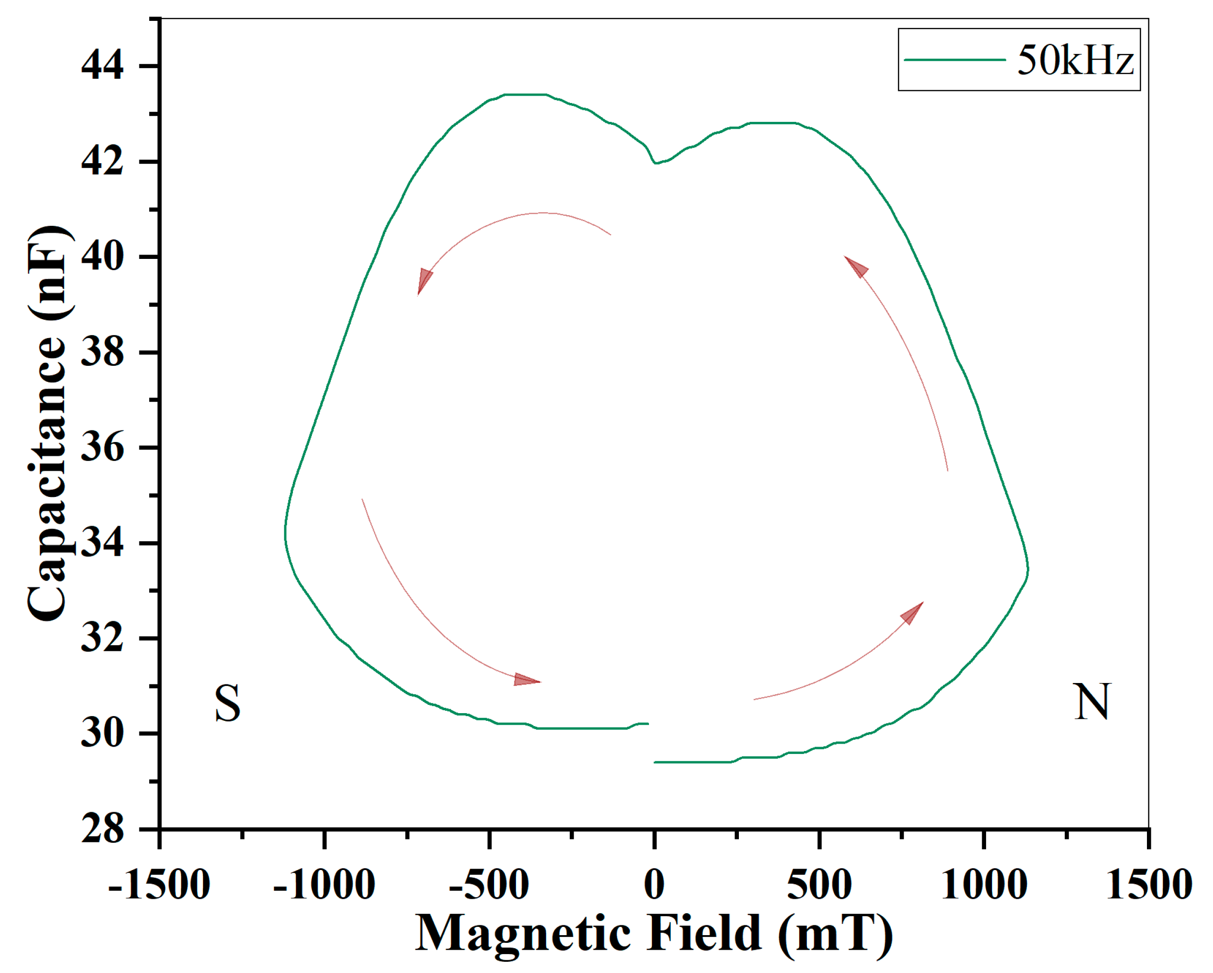
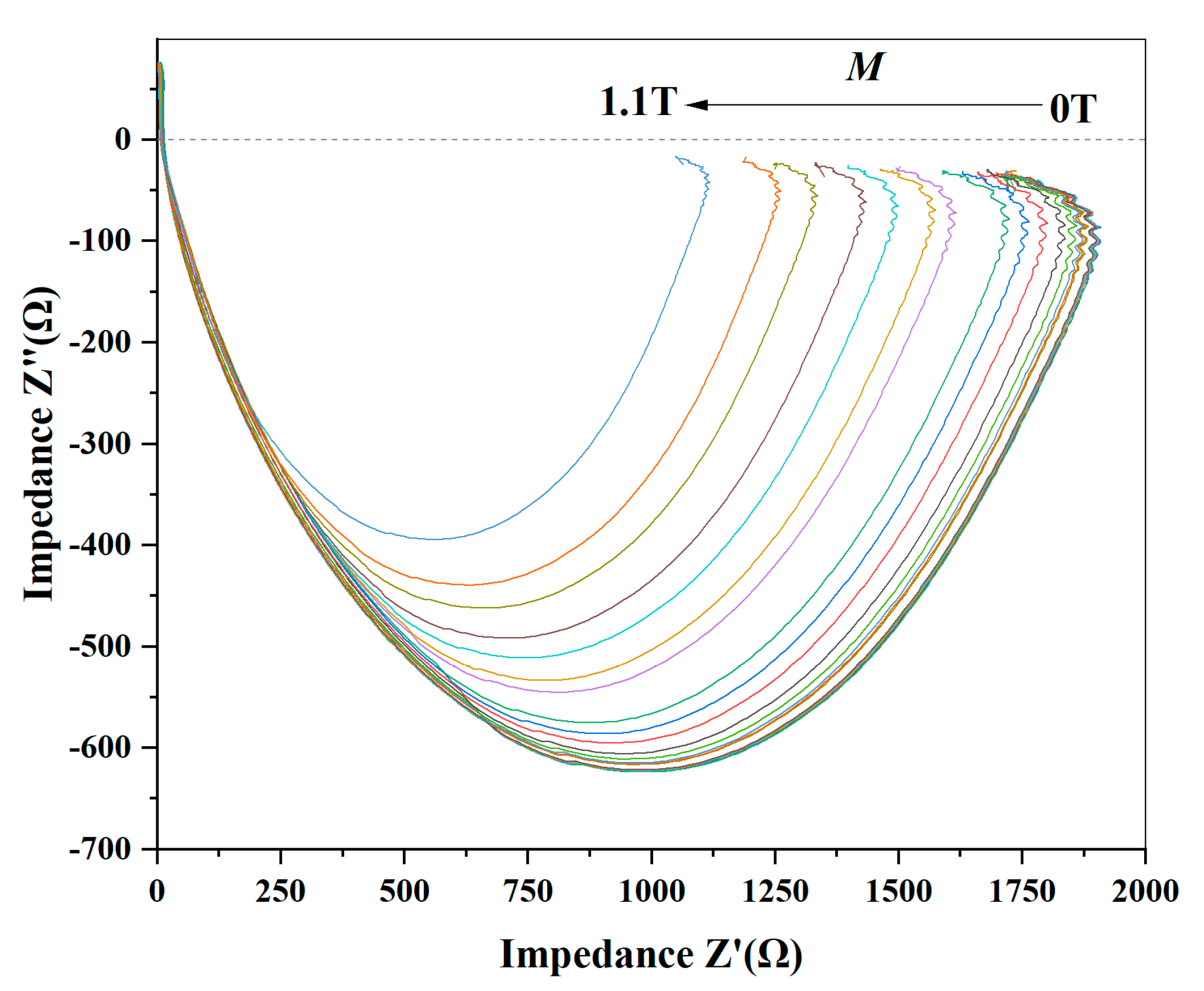
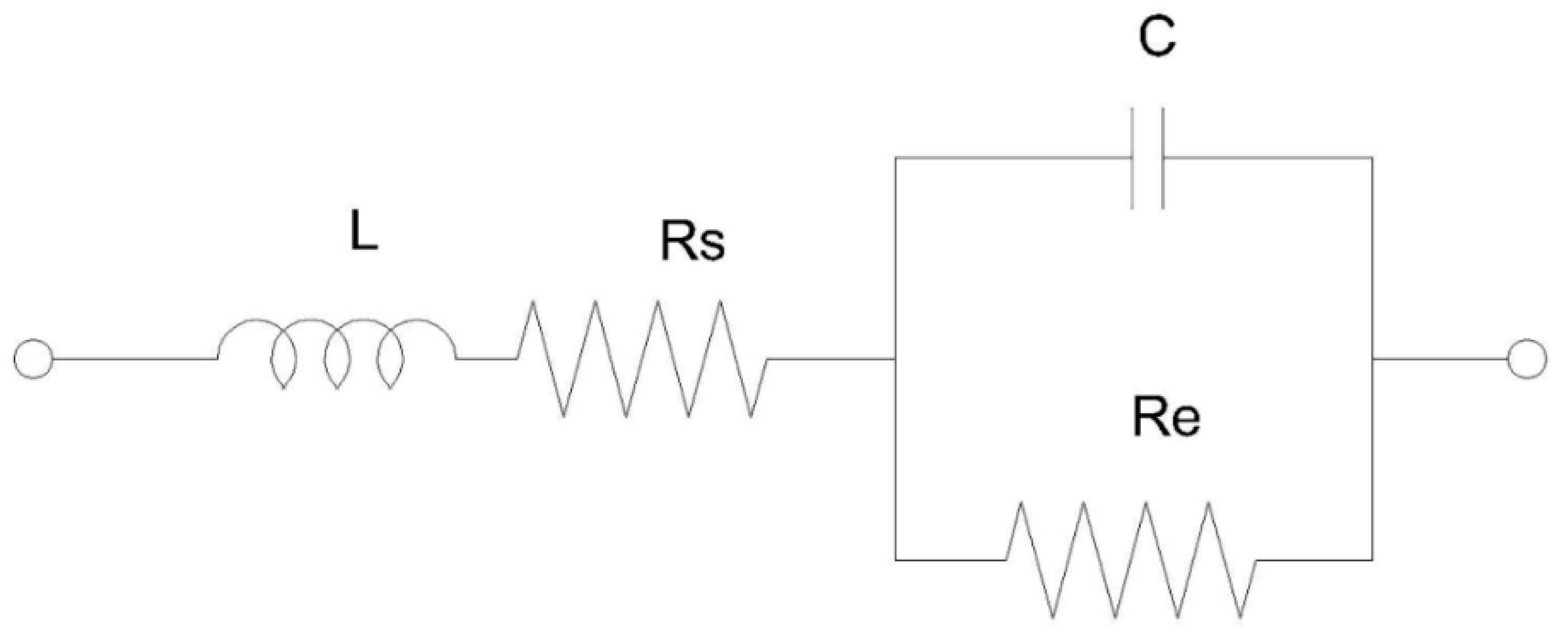
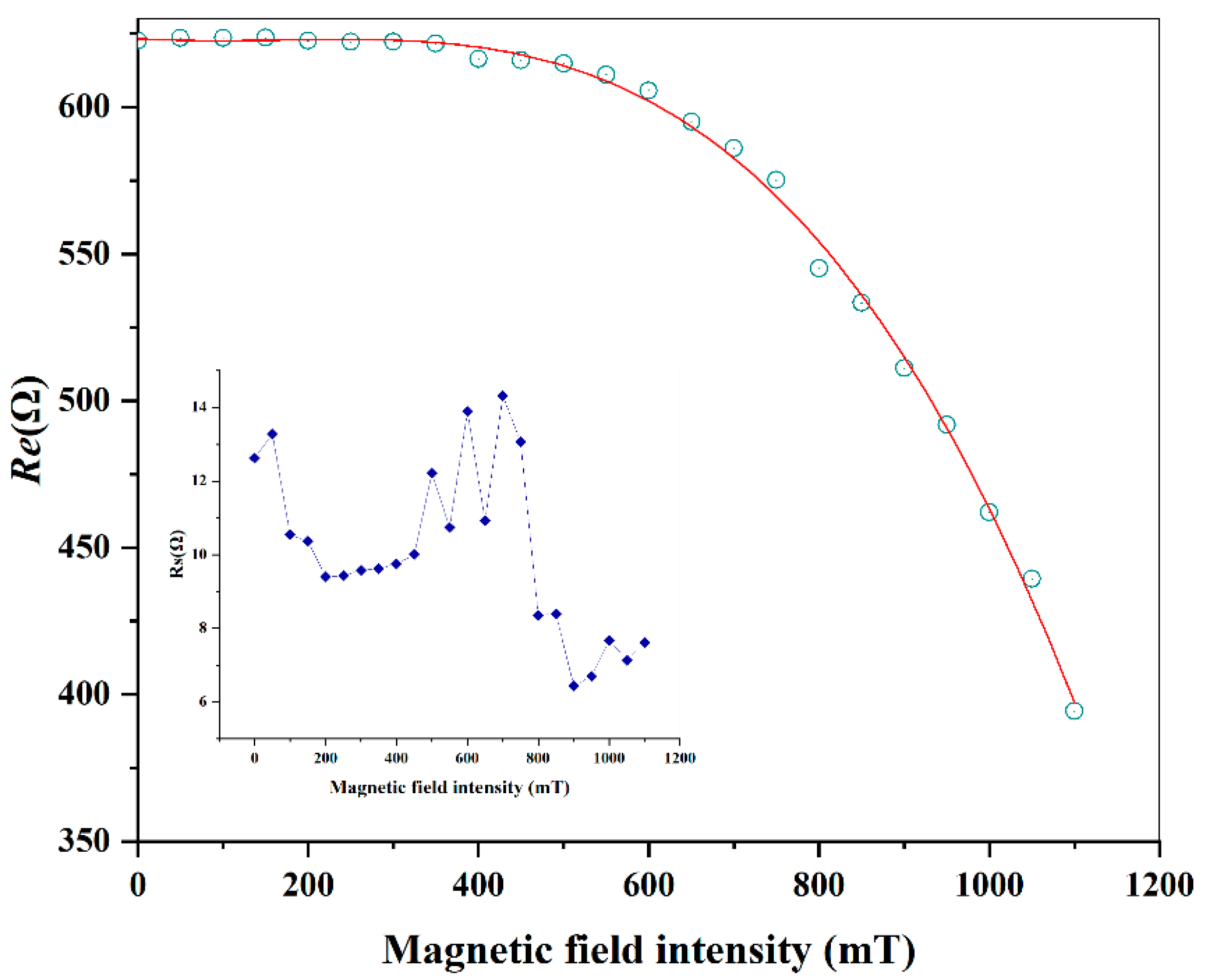
3.5. Magnetoelectric Coupling and GMR Effect of La0.75Ba0.25Fe12O19 Ceramics

First of all, we measured the electrical polarization behavior of La0.75Ba0.25Fe12O19 ceramics under different magnetic fields. The ceramic pellet was placed in a magnetic field whose direction was perpendicular to its surface, and then the magnetic field strength was continuously increased to 1140 mT in a step of 20 mT. After maintaining the magnetic field strength for about 30 s at each stair, the dielectric parameters were output through the LCR meter to the computer. The capacitance varying with the magnetic fields are shown in Figure 10. It can be seen from this figure that when the magnetic field (H) was increasing in the positive direction, the capacitance was increasing accordingly, and the capacitance reached 33.4 nF when the H field increased to 1140 mT. Afterwards, as the magnetic field reversely reduced down to about 360 mT, the capacitance further increased to 42.8 nF. Then, the capacitance began to decrease when the H field further reversely decreased. After the magnetic field weakened to 0 and then increased in the reverse direction, the capacitance started to increase again, until the magnetic field increased to about −360 mT, and the capacitance increased to 43.4 nF again. After that point, the capacitance began to decrease with the increase in the H field. When the magnetic field increased to −1140 mT, the capacitance decreased to 34 nF, and then as the magnetic field went back to 0 mT, the capacitance further decreased to 30.2 nF. The varying track of the capacitance with the recycling H field looked like a hysteresis loop, which could be designated to be a magnetically induced electric polarization (P–H) hysteresis loop, which is similar to a P–E or M–H loop. The change in capacitance with the H field was caused by the magnetoelectric coupling effect, thus forming a pear-loop-shaped diagram as shown in Figure 10.
Since the giant magnetoresistance effect was discovered by Baibich et al. in 1988, the GMR effect has been widely used in hard disk drive (HDD) heads [50]. We measured the complex impedance of La0.75Ba0.25Fe12O19 under different magnetic fields by using a Microtest 6630 LCR meter. We placed the pellet sample coated with silver electrodes on both surface sides in a space between two magnets, whose magnetic field was normal to the surface of the specimen. Then we measured its complex resistance, which changed with the H field under different frequencies. However, if the capacitor was not ideal, it will have parasitic parameters, such as equivalent series inductance ESL and equivalent series resistance ESR, so the capacitor can be simplified as shown in Figure 11. So, the impedance of the actual capacitor can be expressed as:
z = R + j ω L + 1 j ω C = R + j ω L 1 ω C
The modulus of impedance is:
z = R 2 + ω L 1 ω C 2
So, it can be seen from this formula that when the frequency is small, the complex impedance decreases as the frequency increases. This is because the current leads the voltage, which is a typical capacitor charging characteristic, and the capacitive reactance plays a major role, and it is also the part we need to test and deal with. When the frequency increases to about 1 MHz, the complex impedance has an increasing process. This process is due to the excessively high frequency, which causes the voltage to lead the current, which is a typical behavior of inductors applying voltage. When the complex impedance reaches the minimum, the capacitive reactance and the inductive reactance are offset to 0, and the phase of the complex impedance is 0, showing a pure resistance characteristic. We mainly discussed the behavior of La0.75Ba0.25Fe12O19 in the frequency range where capacitive reactance dominated.
The change in complex impedance with different B fields is shown in Figure 12. It can be seen that the complex impedance largely decreased with the increasing the magnetic field at a low frequency, while in the same magnetic field, the complex impedance sharply decreased with the frequency. At 10 Hz, the complex impedance under the 0 T magnetic field was 1682 Ω. As the magnetic field increased to 1.1 T, the complex impedance was reduced to 1065 Ω. The change rate of Z under M (ΔZ = [Z(B)−Z(0)/Z(B)]%) was  − 58%. This MR ratio is similar to the GMR magnitude of Pr0.775Sr0.225MnO3. However, Pr0.775Sr0.225MnO3 shows GMR with this ratio only below −73 °C, while La0.75Ba0.25Fe12O19 demonstrated this GMR ratio at room temperature.
As the magnetic field increases, the complex impedance decreases, causing the real part (Z′) and imaginary part (Z″) of the complex impedance to decrease as the magnetic field increases. However, in the simplified model of the actual capacitor, when the frequency is small, we take the inductor as a path, thus becoming the series connection of the ESR and the ideal capacitor. At this time, the complex impedance can be expressed as z ω = R j 1 ω c = z j z . The impedance complex plane composed of the real part and the imaginary part of the complex impedance should be a straight line with an intercept of R and being perpendicular to the real part of the complex impedance, but the actual impedance complex plane is a semicircle, as shown in Figure 13. This is because the capacitor actually has a dielectric loss resistance R e in parallel with the ideal capacitor C, so the full equivalent circuit of the capacitor is shown in Figure 14. Therefore, the full equivalent circuit can be divided into lead resistances R s that do not vary with frequency, and a parallel circuit of dielectric loss resistors R e and ideal capacitor C. The real and imaginary parts of the complex impedance of the parallel circuit of R e and C can be expressed as a semicircle of expression z R e 2 2 + z 2 = R e 2 2 on the impedance complex plane, but due to the series connection of R s , the complex impedance of the actual capacitor is a semicircle of z R e 2 R s 2 + z 2 = R e 2 2 in the impedance complex plane. It can be seen in Figure 13 that the radius of the Core–Core circle also decreases with the increase in the magnetic field, that is, the lead resistance R s is basically unchanged, while the dielectric loss resistance R e of the capacitor itself decreases with the increase in the magnetic field. This is due to the fact that in the full equivalent model of the actual capacitance in this experiment, the lead resistance R s varies with the magnetic field strength as shown in the inset in Figure 15. The inset shows that the value of R s is small and does not show a clear trend with the magnetic field. While the dielectric loss resistance R e is caused by the sample itself, the value should be closely related to the magnitude of the magnetic field. R e is the radius of the core circle along the x-axis. In order to get closer to the actual value of R e , we processed the lowest point of each core circle in Figure 13 and made its variation with the M-field in Figure 15. As the magnetic field increased, R e changed very little until 600 mT, above which an increase in the magnetic field led to a rapid decrease in R e . These behaviours are more indicative of a GMR effect for La0.75Ba0.25Fe12O19. As the magnetic field increased to 1.1 T, the real part of the complex impedance decreased from 1901 Ω to 1114 Ω, and the imaginary part of the complex impedance decreased from 623 Ω to 394 Ω. It can be seen in Figure 13 that when the imaginary part was greater than 0, the real and imaginary parts of the complex impedance were no longer part of the Core–Core circle. This is because the parasitic inductance had a more significant effect on the complex impedance at higher frequencies.
To derive the maximum value of MR, we treated MR as a function of frequency. Since the value of the complex impedance was very small as the frequency was larger than 300 kHz, and the inductive reactance in the capacitor gradually had a greater impact on the complex impedance, we chose to deal with the change in MR with a frequency below 300 kHz, and the result is shown in Figure 16. It can be seen that the MR increased with the enhancement of the magnetic field, and when the frequency was around 36.7 kHz, the MR reached a maximum of −110.6% at a magnetic field of 1.1 T. However, when the frequency was increased to 40 kHz, the MR ratio gradually became smaller. This feature indicates that the response of the complex impedance to frequency was sensitive. In order to find the direct relationship between the complex impedance and magnetic field strength, we made a graph of the MR ratio versus magnetic field strength at different frequencies of 10 Hz, 100 Hz, 1 kHz, 10 kHz, 36.7 kHz, and 100 kHz. The results are shown in Figure 17. It can be seen that when the magnetic field was less than 600 mT, the slope of MR was basically 0. When the magnetic field was gradually larger than 600 mT, the value of the MR ratio started to gradually increase and the enhancement scale became bigger when the M field increased.
These behaviors can be explained as follows. In the GMR effect of La0.75Ba0.25Fe12O19 ceramics, because the spins of different grains in the ceramics are randomly arranged, the spin-up and spin-down cancel each other in some way, and the electrons passing through each grain will have a certain amount of resistance, so when M = 0, the complex impedance is higher. When the magnetic field is applied, the spins in different directions begin to align in the direction parallel to the magnetic field. However, due to other resistances such as the interaction force between grains, when the magnetic field is small, there is not enough force to overcome the resistance of the material itself, so that the rate of change of the complex reluctance is small when the magnetic field is low. When the strength of the magnetic field increases to a certain level, the spins of the crystal grains begin to gradually accelerate to align in the direction of the magnetic field. Later, when the magnetic field strength becomes stronger and stronger, the spins of more crystal grains complete the alignment in the same direction as the magnetic field direction. In a parallel magnetic structure, electrons with the same spin direction as the magnetic grain can easily pass through the grain, so the impedance through the channel is reduced. The spin of the randomly arranged crystal grains is changed to the same spin with the magnetic field direction by the magnetic field, thereby reducing the resistance of the electrons in the magnetic field direction and increasing the mobility of the electrons. Therefore, when the magnetic field is less than 600 mT, the change rate in the MR of the complex impedance is substantially small, and when the magnetic field is greater than 600 mT, the change rate in the MR of the complex impedance becomes larger and larger.

4. Conclusions

The powder produced by doping lanthanum in BaFe12O19 was examined by XRD to demonstrate that La0.75Ba0.25Fe12O19 was successfully prepared. The behavior of the La0.75Ba0.25Fe12O19 ceramic was examined in an electric field at room temperature, and a double P–E hysteresis loops diagram without macroscopic polarization in the AFE region was successfully obtained. The dielectric loss of La0.75Ba0.25Fe12O19 was measured from −190 °C to 400 °C and the frequency varied from 10 H to 10 MHz. We successfully measured the two phases transition peaks of La0.75Ba0.25Fe12O19 at the frequency of 200 kHz. The TF-A was located at about −184 °C, and TA-P was about 214 °C. Thus, it was concluded that La0.75Ba0.25Fe12O19 was in the AFE phase at room temperature, which was highly consistent with the P–E hysteresis diagram measured at room temperature, and this evidence proves that doping lanthanum into BaFe12O19 can shift its TF-A and TA-P towards lower temperatures, and that the doping of lanthanum makes the FE phase of BaFe12O19 less stable and its AFE phase more stable. This broadens the scope of the study of AFE materials at room temperature. The UV-vis-NIR optical spectrum of La0.75Ba0.25Fe12O19 proved it to be a direct bandgap semiconductor with an E g of 1.753 eV. It is also observed that La0.75Ba0.25Fe12O19 has a distinct M–H hysteresis loop with a remanent magnetization of 23.6 emu/g and a coercivity of 1063.9 Oe. In addition, the compound possesses strong ME coupling and a GMR effect. The maximum MR ratio reached −110.6% when the magnetic field was 1.1 T. In summary, La0.75Ba0.25Fe12O19 is a novel type of multiferroic candidate which combines AFE and FM at room temperature, demonstrating magnetic semiconducting properties, strong ME coupling, and a large GMR effect.

Author Contributions

Writing—original draft preparation, G.-L.T.; writing—review and editing, Z.X. All authors have read and agreed to the published version of the manuscript.

Funding

This research was funded by the National Natural Science Foundation of China under grant No. 11774276.

Institutional Review Board Statement

Not applicable.

Informed Consent Statement

Not applicable.

Data Availability Statement

The data that support the findings of this study are available from the corresponding author upon reasonable request.

Conflicts of Interest

The authors declare no conflict of interest.

References

  1. Chappert, C.; Fert, A.; Van Dau, F.N. The emergence of spin electronics in data storage. Nat. Mater. 2007, 6, 813–823. [Google Scholar] [CrossRef] [PubMed]
  2. Heron, J.T.; Trassin, M.; Ashraf, K.; Gajek, M.; He, Q.; Yang, S.Y.; Nikonov, D.E.; Chu, Y.H.; Salahuddin, S.; Ramesh, R. Electric-Field-Induced Magnetization Reversal in a Ferromagnet-Multiferroic Heterostructure. Phys. Rev. Lett. 2011, 107, 217202. [Google Scholar] [CrossRef] [PubMed]
  3. Rakheja, S.; Flatté, M.E.; Kent, A.D. Voltage-Controlled Topological Spin Switch for Ultralow-Energy Computing: Performance Modeling and Benchmarking. Phys. Rev. Appl. 2019, 11, 054009. [Google Scholar] [CrossRef]
  4. Heron, J.T.; Chiang, T. Magnetoelectrics and multiferroics: Materials and opportunities for energy-efficient spin-based memory and logic. MRS Bull. 2021, 46, 938–945. [Google Scholar] [CrossRef]
  5. Schmid, H. Multi-ferroic magnetoelectrics. Ferroelectrics 1994, 162, 317. [Google Scholar] [CrossRef]
  6. Moskvin, A.S. Microscopic Mechanisms of Magnetoelectric Coupling in 3d Oxides. Solid State Phenom. 2011, 168–169, 445–452. [Google Scholar]
  7. Chang, C.M.; Mani, B.K.; Lisenkov, S.; Ponomareva, I. Thermally Mediated Mechanism to Enhance Magnetoelectric Coupling in Multiferroics. Phys. Rev. Lett. 2015, 114, 177205. [Google Scholar] [CrossRef]
  8. Hu, J.M.; Duan, C.G.; Nan, C.W.; Chen, L.Q. Understanding and designing magnetoelectric heterostructures guided by computation: Progresses, remaining questions, and perspectives. NPJ Comput. Mater. 2017, 3, 18. [Google Scholar] [CrossRef]
  9. Yu, B.; Hu, Z.Q.; Cheng, Y.X.; Peng, B.; Zhou, Z.Y.; Liu, M. Recent progress of multiferroic magnetoelectric devices. Acta Phys. Sin. 2018, 67, 157507. [Google Scholar]
  10. Li, J.; Zhao, D.P.; Bai, H.; Yuan, Z.; Zhou, Z.X. Low magnetic-field induced high temperature dynamic magnetoelectric coupling performances in Z-type Sr3Co2Fe24O41. J. Phys. Condens. Matter 2021, 34, 105803. [Google Scholar] [CrossRef]
  11. De Sousa, R.; Moore, J.E. Multiferroic Materials for Spin-Based Logic Devices. J. Nanoelectron. Optoelectron. 2008, 3, 77–81. [Google Scholar] [CrossRef]
  12. De Sousa, R.; Allen, M.; Cazayous, M. Theory of Spin-Orbit Enhanced Electric-Field Control of Magnetism in Multiferroic BiFeO3. Phys. Rev. Lett. 2013, 110, 267202. [Google Scholar] [CrossRef] [PubMed]
  13. Gopman, D.B.; Chen, P.; Lau, J.W.; Chavez, A.C.; Carman, G.P.; Finkel, P.; Staruch, M.; Shull, R.D. Large Interfacial Magnetostriction in (Co/Ni)4/Pb(Mg1/3Nb2/3)O3–PbTiO3 Multiferroic Heterostructures. ACS Appl. Mater. Interfaces 2018, 10, 24725–24732. [Google Scholar] [CrossRef]
  14. Li, X.; Casamento, J.; Dang, P.; Zhang, Z.; Afuye, O.; Mei, A.B.; Apsel, A.B.; Schlom, D.G.; Jena, D.; Ralph, D.C.; et al. Spin–orbit torque field-effect transistor (SOTFET): Proposal for a magnetoelectric memory. Appl. Phys. Lett. 2020, 116, 242405. [Google Scholar] [CrossRef]
  15. Vopson, M.M. Fundamentals of Multiferroic Materials and Their Possible Applications. Crit. Rev. Solid State Mater. Sci. 2015, 40, 223–250. [Google Scholar] [CrossRef]
  16. Mudinepalli, V.R.; Feng, L.; Lin, W.-C.; Murty, B.S. Effect of grain size on dielectric and ferroelectric properties of nanostructured Ba0.8Sr0.2TiO3 ceramics. J. Adv. Ceram. 2015, 4, 46–53. [Google Scholar] [CrossRef]
  17. Clabel, H.J.L.; Ferri, F.A.; Zabotto, F.L.; Rivera, V.A.G.; Nogueira, I.C.; Garcia, D.; de Lima, O.F.; Leite, E.R.; Pereira-da-Silva, M.A.; Cardoso, C.A. Grain size and interfacial interdiffusion influence on the magnetic and dielectric properties of magnetoelectric La0.7Ba0.3MnO3–BaTiO3 composites. J. Magn. Magn. Mater. 2016, 407, 160–166. [Google Scholar] [CrossRef]
  18. Zhang, Q.W.; Zhai, J.W.; Shen, B.; Zhang, H.J.; Yao, X. Grain size effects on dielectric properties of barium strontium titanate composite ceramics. Mater. Res. Bull. 2013, 48, 973–977. [Google Scholar] [CrossRef]
  19. Han, T.-C.; Hsu, W.-L.; Lee, W.-D. Grain size-dependent magnetic and electric properties in nanosized YMnO3 multiferroic ceramics. Nanoscale Res. Lett. 2011, 6, 201. [Google Scholar] [CrossRef]
  20. Clabel, H.J.L.; Zabotto, F.L.; Nogueira, I.C.; Schio, P.; Garcia, D.; de Lima, O.F.; Leite, E.R.; Moreira, F.M.A.; Cardoso, C.A. Magnetoelectric properties of laminated La0.7Ba0.3MnO3–BaTiO3 ceramic composites. J. Magn. Magn. Mater. 2014, 364, 18–23. [Google Scholar] [CrossRef]
  21. Huamán, J.L.C.; Rivera, V.A.G.; Pinto, A.H.; Marega, E. 11—Multiferroic perovskite ceramics: Properties and applications. In Perovskite Ceramics; Huamán, J.L.C., Rivera, V.A.G., Eds.; Elsevier: Amsterdam, The Netherlands, 2023; pp. 339–381. [Google Scholar]
  22. Teague, J.R.; Gerson, R.; James, W.J. Dielectric hysteresis in single crystal BiFeO3. Solid State Commun. 1970, 8, 1073. [Google Scholar] [CrossRef]
  23. Kimura, T.; Goto, T.; Shintani, H.; Ishizaka, K.; Arima, T.; Tokura, Y. Magnetic control of ferroelectric polarization. Nature 2003, 426, 55–58. [Google Scholar] [CrossRef] [PubMed]
  24. Tokunaga, Y.; Kaneko, Y.; Okuyama, D.; Ishiwata, S.; Arima, T.; Wakimoto, S.; Kakurai, K.; Taguchi, Y.; Tokura, Y. Multiferroic M-type hexaferrites with a room-temperature conical state and magnetically controllable spin helicity. Phys. Rev. Lett. 2010, 105, 257201. [Google Scholar] [CrossRef] [PubMed]
  25. Tan, G.L.; Wang, M. Multiferroic PbFe12O19 ceramics. J. Electroceramics 2011, 26, 170. [Google Scholar] [CrossRef]
  26. Wang, L.; Wang, D.; Cao, Q.; Zheng, Y.; Xuan, H.; Gao, J.; Du, Y. Electric control of magnetism at room temperature. Sci. Rep. 2012, 2, 223. [Google Scholar] [CrossRef]
  27. Zhou, W.P.; Wang, L.Y.; Song, Y.Q.; Fang, Y.; Wang, D.H.; Cao, Q.Q.; Du, Y.W. Magnetoelectric effect in PbCoTiFe10O19 multiferroic ceramic. Ceram. Int. 2014, 40 Pt A, 15737–15742. [Google Scholar] [CrossRef]
  28. Li, X.; Tan, G.L. Multiferroic and magnetoelectronic polarizations in BaFe12O19 system. J. Alloys Compd. 2021, 858, 157722. [Google Scholar] [CrossRef]
  29. Sharma, V.; Kumari, S.; Kuanr, B.K. Rare earth doped M-type hexaferrites; ferromagnetic resonance and magnetization dynamics. AIP Adv. 2018, 8, 056232. [Google Scholar] [CrossRef]
  30. Yousaf, M.; Nazir, S.; Hayat, Q.; Akhtar, M.N.; Akbar, M.; Lu, Y.; Noor, A.; Zhang, J.M.; Shah, M.A.K.Y.; Wang, B. Magneto-optical properties and physical characteristics of M-type hexagonal ferrite (Ba1-xCaxFe11.4Al0.6O19) nanoparticles (NPs). Ceram. Int. 2021, 47, 11668–11676. [Google Scholar] [CrossRef]
  31. Guerra, J.D.S.; Betal, S.; Pal, M.; Garcia, J.E.; Oliveira, A.J.A.; M’Peko, J.C.; Hernandes, A.C.; Guo, R.Y.; Bhalla, A.S. Magnetoelectric Response in (1-x)PbZr0.65Ti0.35O3-xBaFe12O19 Multiferroic Ceramic Composites. J. Am. Ceram. Soc. 2015, 98, 1542–1547. [Google Scholar] [CrossRef]
  32. Vinnik, D.A.; Podgornov, F.V.; Zabeivorota, N.S.; Trofimov, E.A.; Zhivulin, V.E.; Chernukha, A.S.; Gavrilyak, M.V.; Gudkova, S.A.; Zherebtsov, D.A.; Ryabov, A.V.; et al. Effect of treatment conditions on structure and magnetodielectric properties of barium hexaferrites. J. Magn. Magn. Mater. 2020, 498, 166190. [Google Scholar] [CrossRef]
  33. Vinnik, D.A.; Zhivulin, V.E.; Starikov, A.Y.; Gudkova, S.A.; Trofimov, E.A.; Trukhanov, A.V.; Trukhanov, S.V.; Turchenko, V.A.; Matveev, V.V.; Lahderanta, E.; et al. Influence of titanium substitution on structure, magnetic and electric properties of barium hexaferrites BaFe12−xTixO19. J. Magn. Magn. Mater. 2020, 498, 166117. [Google Scholar] [CrossRef]
  34. Chun, S.H.; Chai, Y.S.; Oh, Y.S.; Jaiswal Nagar, D.; Haam, S.Y.; Kim, I.; Lee, B.; Nam, D.H.; Ko, K.T.; Park, J.H.; et al. Realization of Giant Magnetoelectricity in Helimagnets. Phys. Rev. Lett. 2010, 104, 037204. [Google Scholar] [CrossRef] [PubMed]
  35. Wang, F.; Zou, T.; Yan, L.Q.; Liu, Y.; Sun, Y. Low magnetic field reversal of electric polarization in a Y-type hexaferrite. Appl. Phys. Lett. 2012, 100, 122901. [Google Scholar] [CrossRef]
  36. Samara, G.A. Pressure and temperature dependence of the dielectric properties and phase transition of the antiferroelectric perovskites: PbZrO3 and PbHfO3. Phys. Rev. B 1970, 1, 3777–3786. [Google Scholar] [CrossRef]
  37. Zhelnova, O.A.; Fesenko, O.E. Phase transitions and twinning in NaNbO3 crystals. Ferroelectrics 1987, 75, 469–475. [Google Scholar] [CrossRef]
  38. Hao, X.H.; Zhai, J.W.; Kong, L.B.; Xu, Z.K. A comprehensive review on the progress of lead zirconate-based antiferroelectric materials. Prog. Mater. Sci. 2014, 63, 1–57. [Google Scholar] [CrossRef]
  39. Pan, M.J.; Markowski, K.A.; Park, S.E.; Yoshikawa, S.; Cross, L.E. Antiferroelectric-to-ferroelectric phase switching PLSnZT ceramics. I. Structure, compositional modification and electrical properties. In Proceedings of the Tenth IEEE International Symposium on Applications of Ferroelectrics, East Brunswick, NJ, USA, 18–21 August 1996; Volume 1, pp. 267–270. [Google Scholar]
  40. Bharadwaja, S.S.N.; Laha, A.; Halder, S.; Krupanidhi, S.B. Reversible and irreversible switching processes in pure and lanthanum modified lead zirconate thin films. Mater. Sci. Eng. B 2002, 94, 218–222. [Google Scholar] [CrossRef]
  41. Bharadwaja, S.S.N.; Saha, S.; Bhattacharyya, S.; Krupanidhi, S.B. Dielectric properties of La-modified antiferroelectric PbZrO3 thin films. Mater. Sci. Eng. B 2002, 88, 22–25. [Google Scholar] [CrossRef]
  42. Bharadwaja, S.S.N.; Krupanidhi, S.B. Study of La-modified antiferroelectric PbZrO3 thin films. Thin Solid Film. 2003, 423, 88–96. [Google Scholar] [CrossRef]
  43. Yamashita, T.; Hayes, P. Analysis of XPS spectra of Fe2+ and Fe3+ ions in oxide materials. Appl. Surf. Sci. 2008, 254, 2441–2449. [Google Scholar] [CrossRef]
  44. Bagus, P.S.; Nelin, C.J.; Brundle, C.R.; Crist, B.V.; Lahiri, N.; Rosso, K.M. Combined multiplet theory and experiment for the Fe 2p and 3p XPS of FeO and Fe2O3. J. Chem. Phys. 2021, 154, 094709. [Google Scholar] [CrossRef]
  45. Van Doveren, H.; Verhoeven, J.A.T.H. XPS spectra of Ca, Sr, Ba and their oxides. J. Electron Spectrosc. Relat. Phenom. 1980, 21, 265–273. [Google Scholar] [CrossRef]
  46. Ivanova, O.P.; Naumkin, A.V.; Vasilyev, L.A. An XPS study of compositional changes induced by argon ion bombardment of the LaPO4 surface. Vacuum 1996, 47, 67–71. [Google Scholar] [CrossRef]
  47. Dai, X.; Viehland, D. Effects of lanthanum modification on the antiferroelectric-ferroelectric stability of high zirconium-content lead zirconate titanate. J. Appl. Phys. 1994, 76, 3701–3709. [Google Scholar] [CrossRef]
  48. Xu, Z.; Dai, X.; Viehland, D. Impurity-induced incommensuration in antiferroelectric La-modified lead zirconate titanate. Phys. Rev. B 1995, 51, 6261–6271. [Google Scholar] [CrossRef]
  49. Viehland, D.; Dai, X.H.; Li, J.F.; Xu, Z. Effects of quenched disorder on La-modified lead zirconate titanate: Long- and short-range ordered structurally incommensurate phases, and glassy polar clusters. J. Appl. Phys. 1998, 84, 458–471. [Google Scholar] [CrossRef]
  50. Hirohata, A.; Takanashi, K. Future perspectives for spintronic devices. J. Phys. D: Appl. Phys. 2014, 47, 193001. [Google Scholar] [CrossRef]
Figure 1. (A) Unprocessed XRD spectrum. (B) XRD spectra processed with Rietveld refinement. (a) XRD spectrum of La0.75Ba0.25Fe12O19 powders, which were sintered at 1400 °C for 3 h and subsequently annealed in an O2 atmosphere at 800 °C for 15 h in 3 steps, and (b) standard XRD spectrum of the BaFe12O19 (PDF#84-0757) in discrete red lines.
Applsci 13 05718 g001
Figure 2. SEM images of a La0.75Ba0.25Fe12O19 ceramic specimen, which was sintered at 1400 °C for 3 h and subsequently annealed in an O2 atmosphere at 800 °C for 15 h in 3 steps.
Applsci 13 05718 g002
Figure 3. The energy dispersive spectrum (EDS) of La0.75Ba0.25Fe12O19 ceramic specimen.
Applsci 13 05718 g003
Figure 4. (A) XPS survey spectrum of La0.75Ba0.25Fe12O19; XPS spectra of Fe 2p (B), La 3d (C), and Ba 3d (D) in La0.75Ba0.25Fe12O19.
Applsci 13 05718 g004
Figure 5. The fully separated double electric polarization hysteresis (PE) loops of La0.75Ba0.25Fe12O19 ceramic. The ceramic was sintered at 1400 °C for 3 h and subsequently heat-treated in O2 for 15 h in 3 steps.
Applsci 13 05718 g005
Figure 6. Recoverable energy density of La0.75Ba0.25Fe12O19 ceramics under different electric fields; the inset shows one more double P–E hysteresis loop obtained from a different La0.75Ba0.25Fe12O19 ceramic specimen.
Applsci 13 05718 g006
Figure 7. Temperature-dependent dielectric loss spectrum of La0.75Ba0.25Fe12O19 ceramics in the range of −190 °C to 400 °C (frequency changes from 50 kHz to 900 kHz in the low temperature region, while it varies from 50 kHz to 200 kHz only in the high-temperature region).
Applsci 13 05718 g007
Figure 8. (A) UV-vis-NIR optical spectrum of La0.75Ba0.25Fe12O19 ceramics. (B) Tauc plot of α h v 2 versus h v for La0.75Ba0.25Fe12O19 ceramics.
Applsci 13 05718 g008
Figure 9. Magnetic hysteresis loops of La0.75Ba0.25Fe12O19 specimen.
Applsci 13 05718 g009
Figure 10. Variation diagram of the capacitance of La0.75Ba0.25Fe12O19 ceramics under different magnetic fields.
Applsci 13 05718 g010
Figure 11. Simplified model of actual capacitance. ESR is the equivalent series resistance, ESL is the equivalent series inductance, and C is the ideal capacitance.
Applsci 13 05718 g011
Figure 12. Variation of complex impedance with frequency for La0.75Ba0.25Fe12O19 ceramics under different M fields.
Applsci 13 05718 g012
Figure 13. The Core–Core circle formed by the real and imaginary parts of the impedance as the M-field changed.
Applsci 13 05718 g013
Figure 14. The full equivalent circuit of the actual capacitor. R s is the lead resistance, ESL is the equivalent series inductance, R e is the dielectric loss resistance, and C is the ideal capacitance.
Applsci 13 05718 g014
Figure 15. Variation in dielectric loss resistance R e with magnetic field strength. The inset in the figure corresponds to the curve of the lead resistance R s as a function of the magnetic field strength.
Applsci 13 05718 g015
Figure 16. Trend of MR (Z(B)−Z(0)/Z(B))% from 10 Hz to 300 kHz as the M field changes; (a) 0 mT, (b) 50 mT, (c) 100 mT, (d) 150 mT, (e) 200 mT, (f) 250 mT, (g) 300 mT, (h) 350 mT, (i) 400 mT, (j) 450 mT, (k) 500 mT, (l) 550 mT, (m) 600 mT, (n) 650 mT, (o) 700 mT, (p) 750 mT, (q) 800 mT, (r) 850 mT, (s) 900 mT, (t) 950 mT, (u) 1000 mT, (v) 1050 mT, (w) 1100 mT.
Applsci 13 05718 g016
Figure 17. The trends of MR with the magnetic field strength at frequencies of 10 Hz, 100 Hz, 1 kHz, 10 kHz.
Applsci 13 05718 g017
Disclaimer/Publisher’s Note: The statements, opinions and data contained in all publications are solely those of the individual author(s) and contributor(s) and not of MDPI and/or the editor(s). MDPI and/or the editor(s) disclaim responsibility for any injury to people or property resulting from any ideas, methods, instructions or products referred to in the content.

