Article

An Optimized Hardware Implementation of a Non-Adjacent Form Algorithm Using Radix-4 Multiplier for Binary Edwards Curves

1
Deanship of Scientific Research, Umm Al Qura University, Makkah 21955, Saudi Arabia
2
Computer Engineering Department, Umm Al Qura University, Makkah 21955, Saudi Arabia
3
Computer Science Department, Umm Al Qura University, Makkah 21955, Saudi Arabia
*
Authors to whom correspondence should be addressed.
Appl. Sci. 2024, 14(1), 54; https://doi.org/10.3390/app14010054
Submission received: 15 October 2023 / Revised: 27 November 2023 / Accepted: 11 December 2023 / Published: 20 December 2023

Abstract

:
Binary Edwards Curves (BEC) play a pivotal role in modern cryptographic processes and applications, offering a combination of robust security as well as computational efficiency. For robust security, this article harnesses the inherent strengths of BEC for the cryptographic point multiplication process by utilizing the Non-Adjacent Form (NAF) algorithm. For computational efficiency, a hardware architecture for the NAF algorithm is proposed. Central to this architecture is an Arithmetic Logic Unit (ALU) designed for streamlined execution of essential operations, including addition, squaring, and multiplication. One notable innovation in our ALU design is the integration of multiplexers, which maximize ALU efficiency with minimal additional hardware requirements. Complementing the optimized ALU, the proposed architecture incorporates a radix-4 multiplier, renowned for its efficiency in both multiplication and reduction. It eliminates resource-intensive divisions, resulting in a substantial boost to overall computational speed. The architecture is implemented on Xilinx Virtex series Field-Programmable Gate Arrays (FPGAs). It achieves throughput-to-area ratios of 14.819 (Virtex-4), 25.5 (Virtex-5), 34.58 (Virtex-6), and 37.07 (Virtex-7). These outcomes underscore the efficacy of our optimizations, emphasizing an equilibrium between computational performance and area utilization.

1. Introduction

Cryptography is the science of encoding information to safeguard its confidentiality and integrity. It is pivotal in achieving a secure and protected environment [1]. Over the years, various cryptographic techniques have emerged. Each technique/algorithm has its own strengths and weaknesses [2,3]. In this context, Elliptic Curve Cryptography (ECC) is regarded as a method that strikes good balance between security and efficiency [4]. Due to its ability to operate effectively with smaller key sizes and low computing requirements, it has become a popular option for devices and applications with limited resources. This includes Internet of Things (IoT) devices and secure communication protocols [5].
Despite the numerous advantages of ECC, it does present challenges. One of the major drawbacks of ECC lies in its vulnerability to Side-Channel Power Analysis (SPA) attacks [6]. SPA attacks exploit variations in a device’s power consumption to infer sensitive information such as cryptographic keys. To address vulnerability to SPAs, cryptographic algorithms often require advanced countermeasures [7]. A typical example of these countermeasures is the employment of NAF representation during the point multiplication [8,9,10] process. Point multiplication is one of the most computational processes in any type of elliptic curve. Therefore, by utilizing the NAF algorithm, the number of additions and subtractions needed for point multiplication is reduced, consequently minimizing the vulnerability to SPA attacks.
This article introduces a novel hardware architecture design for the implementation of the NAF algorithm. Moreover, the introduced architecture in this article leverages unified mathematical formulations. A variety of elliptic curves provide unified mathematical formulations, including binary Huff curves (BHCs) [11], Hessian curves (HCs) [12], and binary Edwards curves (BECs) [13]. Nevertheless, the proposed architecture adopts BECs for unified mathematical formulations. BECs were chosen because of their effective arithmetic operations and acceptable security characteristics. They are the perfect match for our design since they ensure high-performance calculations while offering a solid foundation for secure ECC. In the following, state-of-the-art hardware architectures for BECs are presented.

1.1. Related Work

The efficiency of point multiplication operations on BECs utilizing FPGAs has improved significantly in the last several years. In this regard, one of the initial works is presented in [14], where a reconfigurable cryptoprocessor is designed. The system operates at a frequency of 48 MHz. However, it heavily utilizes hardware resources, consuming 21,816 slices. This resource utilization increases to 22,373 slices when performing BEC operations with halving. It ultimately limits its suitability for resource-constrained embedded devices. Consequently, a compromise between computational efficiency (latency) and area utilization is required.
A pipelined digital-serial multiplier is presented in [15] for a better compromise between computational efficiency and area utilization, and the corresponding performance figures are presented for the Virtex-5 platform. As a result, the latency of the point multiplication operation is reduced to 11.03 microseconds with the utilization of 8875 slices. Another architecture, targeting the optimization of latency and area, is presented in [16]. The authors introduced two architectures that leverage a comb Parallel Multiplier (PM) technique. The first architecture targets low complexity and achieves enhancements of 62%, 46%, and 152% for G F ( 2 233 ) , G F ( 2 163 ) , and G F ( 2 283 ) , respectively. The second architecture targets low latency and achieves improvements of 55%, 44%, and 76% for G F ( 2 233 ) , G F ( 2 163 ) , and G F ( 2 283 ) , respectively.
The work in [17] is based on a modular radix-2 interleaved multiplier. The objective is to reduce the computing time, the required number of clock cycles, and area requirements. To achieve this, the architecture employs the Montgomery ladder algorithm. However, the authors did not specify the curve parameters where their hardware design presents the best and worst performance. It implies that performance results are not presented for different curve parameters. Similarly, the work in [18] focuses on the optimization of throughput and area at the same time. It introduces two architectures. The first is tailored for general BECs, while the second is specifically designed for special BECs. The optimizations are based on advanced finite field multiplication techniques. Therefore, a trade-off between area and computational efficiency is obtained. The architecture employs three parallel multipliers for better computational efficiency but at the cost of increased hardware resources. Specifically, for curve parameters d 1 and d 2 equal to 59, the area is reduced to 4454 slices. To optimize the area even further, the architecture is modified, employing only two multipliers. Consequently, the area is reduced to 3521 slices while maintaining acceptable latency levels.
In the context of area optimization, authors in [19] optimize the architecture by introducing a digital-serial multiplier. This leads to the utilization of 2138 slices for the Virtex-6 platform and 2153 slices for the Virtex-5 platform. While this architecture achieves area optimization, it compromises the speed of the system. The work in [20] also focuses on resource optimization. The architecture incorporates a digital parallel least significant multiplier. Along with the effective multiplication, point multiplication instructions are carefully organized. The synthesis results are presented across multiple platforms. The limitation is the lack of a thorough analysis of the results regarding computational speed, leaving the potential for additional investigation in this area.
Finally, the authors in [21] propose a hybrid algorithm for the optimization of BEC computations. The hybrid technique combines Montgomery and double-and-add techniques. Moreover, clock cycles are optimized by utilizing a modular Montgomery radix multiplier. The limitation is the absence of adaptability. It implies that the architecture is not explored for various security requirements and multiple complex scenarios.

1.2. Research Gap

Section 1.1 reveals that the performance enhancement of point multiplication on BECs has optimized latency, area, and throughput. Nevertheless, the following points need further exploration:
  • Scalability and Adaptability: It is not well understood how existing architectures perform when dealing with various sizes of curves as well as different levels of security.
  • Resource Efficiency versus Speed Trade-off: Balancing computational speed and hardware resource utilization needs further exploration, especially for resource-constrained devices.
  • Detailed Performance Metrics: Many studies lack an evaluation of performance metrics including speed, which is crucial when making design choices.
Consequently, a hardware architecture is needed that can effectively utilize BEC for PM operation through some algorithmic and architectural innovations.

1.3. Contributions

In order to address the highlighted research gap in Section 1.2, the contributions of this article are summarized as follows:
  • The first contribution is the effective utilization of BECs for cryptographic computations through the innovative application of the NAF algorithm. It ensures robust security and computational efficiency. The utilization of the NAF technique for point multiplication on BECs successfully fills the research gap concerning scalability and adaptability. The NAF algorithm presents a versatile method that may be applied to different curve sizes and levels of security. Our architecture is adaptable and scalable, as evidenced by achieved results, showing strong performance over a range of curve parameters.
  • The second contribution is the optimization of the Arithmetic Logic Unit (ALU) within the hardware design, maximizing ALU efficiency with minimal additional hardware. Moreover, the incorporation of a radix-4 multiplier eliminates resource-intensive divisions and substantially boosts computational speed while reducing hardware complexity. The trade-off between resource efficiency and speed is addressed by the integration of a radix-4 multiplier and the optimization of the Arithmetic Logic Unit (ALU). Our design minimizes the use of hardware resources while carefully balancing processing speed. Rapid cryptographic operations are facilitated by the radix-4 multiplier, which is renowned for its speed benefits, and the optimized ALU, which guarantees efficient operations. Our approach achieves an optimal equilibrium with great progress, especially useful for devices with limited resources.
  • Finally, to perform cryptographic operations with precision, our design integrates a Finite State Machine (FSM). This FSM is designed for an optimal control flow, minimizing latency, and managing system resources, thus optimizing overall performance.
To summarize, the proposed framework presents a substantial advancement in ECC, improving both security and computational efficiency. Our design provides a reliable ECC solution through the creative application of the NAF algorithm for PM on BEC. The NAF method streamlines processes and speeds up computations by lowering the amount of nonzero digits. Lowering the possibility of side-channel attacks improves security. Additionally, our design utilizes 2 × 1 multiplexers to optimize the ALU. While the area is slightly increased, throughput is significantly increased. The integration of NAF and ALU optimization ensures not only better security measures but also improved computational speed.

1.4. Organization

The structure of this article is organized to provide readers with a systematic understanding of the presented research. Section 2 establishes a strong foundation by elucidating the mathematical background of BEC. Section 3 delves into the core of our contributions, where we detail the proposed hardware architecture. This section introduces readers to the key components of our design. Moreover, it also offers insights into the design considerations and intricate implementation aspects. Section 4 is dedicated to our proposed optimizations, particularly focusing on scheduling techniques. It presents a thorough exploration of how we fine-tuned our architecture for optimal performance. Section 5 presents the main findings and results derived from a rigorous analysis. It allows for readers to gauge the efficiency and efficacy of our design in relation to existing solutions. Finally, Section 6 summarizes key takeaways and suggests intriguing directions for future investigations.

2. Setting the Stage: Fundamental Mathematics and Knowledge

The basic mathematics required to understand the fundamentals of BEC are given in Section 2.1. The elaboration on the fundamentals of BEC is further extended in Section 2.2 by describing its unified mathematical formulations. Finally, the computation of the point multiplication process with the NAF algorithm is illustrated in Section 2.3.

2.1. Fundamentals of BEC

The work in [22] presented the BEC model introducing the mathematical formulations for BEC within a prime field. Consequently, the BEC model within a prime field can be represented by the following equation:
x 2 + y 2 = 1 + d x 2 y 2 .
Equation (1) defines the curve with variables x, y, and d. Here, variables x and y are the starting points whereas variable d indicates a curve parameter. It is important to note that the handling of curves with relatively larger prime fields is a challenging task. Addressing this concern, the work in [23] presented a binary variant of Edwards curves. Consequently, the binary variant of Edwards curves can be shown by the following equation:
E B , d 1 , d 2 : d 1 ( x + y ) + d 2 ( x 2 + y 2 ) = x y + x y ( x + y ) + x 2 y 2 .
Equation (2) is the mathematical form of BEC, incorporating initial points x and y, along with curve parameters d 1 and d 2 . Notably, Equation (2) holds true only when d 1 is a number other than zero and d 2 is not equal to d 1 2 + d 1 . In addition to the mathematical formulations, working with BEC requires taking into account the following fundamental notions. First, the binary aspect of digital systems is reflected in binary fields, which use bitwise XOR and AND operations, whereas prime fields use conventional arithmetic operations with modulo computations. Second, curve parameters, represented by variables like d 1 and d 2 , are important because they have a major impact on how the elliptic curve behaves. In addition to defining the curve, these parameters affect the computing efficiency and security in cryptographic operations. Appropriate parameter selection is essential since it directly affects how security and performance are balanced in BEC applications.

2.2. Unified Mathematical Formulation

Table 1 presents a set of seven important instructions for the computation of the BEC. The first column shows the essential instructions, while the second column articulates the requisite mathematical formulations for each of them. The initial values, or the system’s initial state, are stored in variables W 1 , Z 1 , W 2 , and Z 2 . On the other hand, W d , Z d , W a , and Z a are used to hold onto the final projective points. Variables A, B, and C effectively store intermediate results. Consequently, the initial, intermediate, and final values are designated as ( W 1 , W 2 , Z 1 , Z 2 ), (A, B, C), and ( W d , Z d , W a , Z a ), respectively. For an effective management of these initial, intermediate, and final values, a total of 11 × m storage units are required. The number 11 signifies the stipulated storage units, with m representing their individual width. Moreover, parameters e 1 , e 2 , and w outlined in Table 1 play instrumental roles in shaping the curve’s operations. These parameters orchestrate vital functions such as point multiplication, doubling, and addition, contributing to both operational efficiency and security enhancement. Parameter e 1 is computed as the fourth root of a specific constant, e, denoted as e 1 = e 4 . Similarly, e 2 signifies the square root of e, calculated as e 2 = e . This constant e finds its composition from the combination of terms d 1 4 , d 1 3 , and d 1 2 d 2 formulated as e = d 1 4 + d 1 3 + d 1 2 d 2 . Furthermore, parameter w consists of a rational function that simplifies computations through expression w ( P ) = x + y d 1 ( x + y + 1 ) , where P = ( x , y ) belongs to the specific elliptic curve E B , d 1 , d 2 .

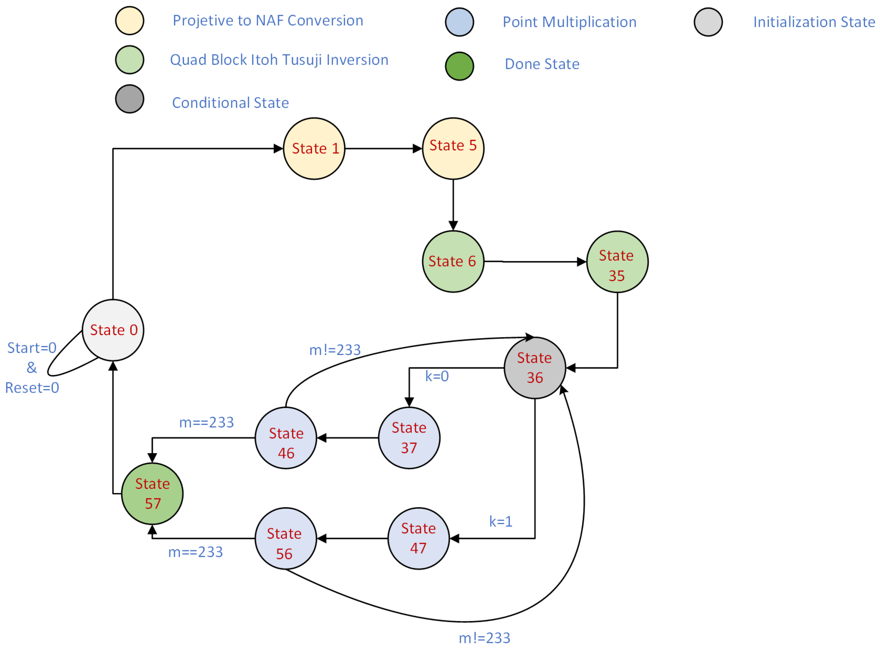
2.3. Computation of the PM Process with the NAF Algorithm

The computations for the PM process can be formulated as [24]
Q = k . p = k ( p + p + , , + p ) .
Variable Q in Equation (3) depicts the endpoint. Similarly, the value of k represents a scalar multiplier while p is the initial point. Algorithm 1, known as the point multiplication with NAF, is employed for the execution of the PM process. The core of the algorithm lies in the efficient execution of point multiplication on a BEC within field G F ( 2 m ) . The input parameters are expressed as E B , d 1 , d 2 / G F ( 2 m ) , where B, d 1 , and d 2 characterize the curve’s attributes. Additionally, the algorithm requires a foundational base point P and a scalar k expressed as a binary sequence, ( k m 1 , , k 1 , k 0 ) . The algorithm’s primary aim revolves around the computation of the resultant point Q. Using NAF methodology, it is obtained by multiplying the base point P with the scalar k. The algorithm employs the following key steps:
Algorithm 1: Point Multiplication with NAF
Applsci 14 00054 i001

2.3.1. Initialization

Critical variables for projective coordinates are initialized at the start of the method. These coordinates, denoted as ( W 1 : Z 1 ) and ( W 2 : Z 2 ) , play a crucial role in the calculations. More specifically, Z 1 is initialized to one and W 1 is initialized to zero. As opposed to this, W 2 and Z 2 are given the values of w ( P ) , requiring calculations based on the coordinates of base point P. This initialization forms the basis for subsequent operations.

2.3.2. Scalar Conversion to NAF

The scalar k is translated into its NAF representation in this stage. This conversion entails a series of iterations. The algorithm determines, at each transition, whether the value of n, which was previously defined as a scalar k, is divisible by two. If there is a NAF representation, a binary “0” is simply appended to it to reduce n by half. If n is odd, the algorithm updates n and adds a residual (“1”) to the NAF. The algorithm, however, skips this step if n is even. The scalar k undergoes an iterative procedure until it hits zero, leading to its NAF representation in the end.

2.3.3. Primary Loop

With NAF representation at hand, the algorithm proceeds into the primary loop. For each bit in the NAF representation (initiating from the leftmost bit),
  • the algorithm performs a “differential addition” operation on points ( W 1 : Z 1 ) and ( W 2 : Z 2 ) . This operation, denoted as d A D D ( ( W 1 : Z 1 ) , ( W 2 : Z 2 ) ) , modifies these points as required;
  • in cases where the current bit within the NAF representation is ‘’1”, an additional “differential addition” operation is executed, involving points ( W 2 : Z 2 ) and ( W 1 : Z 1 ) ;
  • The algorithm activates an inner loop that handles the windowing approach in order to optimize the procedure. Operation optimization using “double-and-add” operations is part of this method. The inner loop spans previous bits of the NAF representation, covering up to w bits in reverse order. Within this loop,
    points ( W 1 : Z 1 ) and ( W 2 : Z 2 ) are updated through the “double-and-add” operation, as represented by d b L ( ( W 1 : Z 1 ) , ( W 2 : Z 2 ) ) ;
    if the bit corresponding to the current iteration within the inner loop is ‘1’, an additional “differential addition” operation occurs for points ( W 2 : Z 2 ) and ( W 1 : Z 1 ) .

2.3.4. End of Loop

As the loops conclude, the algorithm provides the final points, ( W 1 : Z 1 ) and ( W 2 : Z 2 ) , as the output. These points encapsulate the resultant point Q that stems from the adept application of the NAF technique.

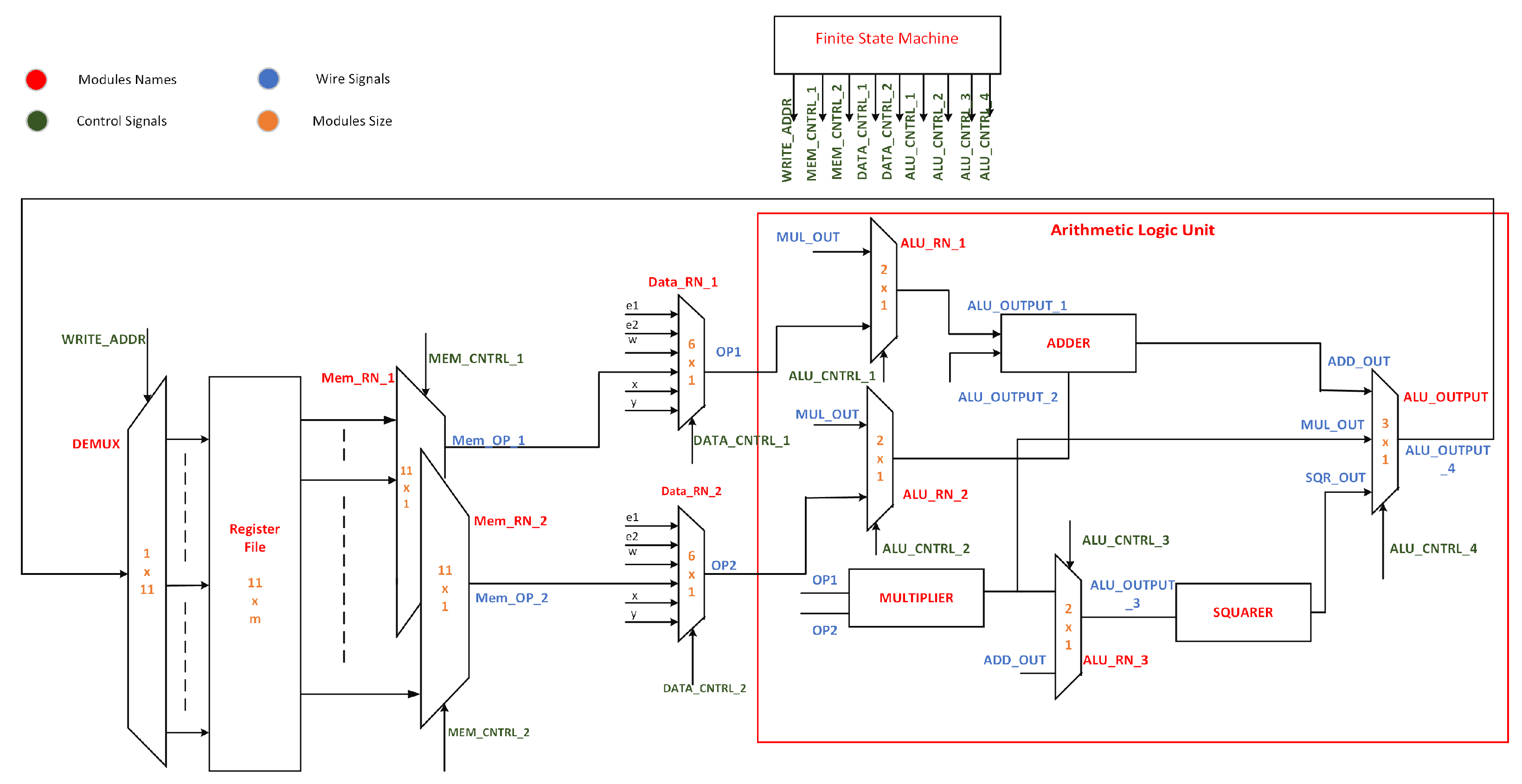
3. Proposed Hardware Architecture

The proposed BEC hardware architecture is shown in Figure 1, illustrating its major components. The description of the major components is organized as follows: Section 3.1 explains the role of the memory unit within the system by illustrating efficient data storage and retrieval mechanisms. Section 3.2 describes multiplexers employed for routing purposes. The description includes a detailed analysis of their function in optimizing data flow and ensuring seamless communication between different parts of the system. Section 3.3 provides an in-depth explanation of the Arithmetic Logic Unit (ALU). It is the core component responsible for executing a diverse range of arithmetic operations essential for cryptographic computations. Section 3.4 introduces the controller, which takes the form of a Finite State Machine (FSM). It optimizes the overall functionality of the BEC architecture. Finally, the clock cycle information is provided in Section 3.5. The architectural design process was conducted using parameters stipulated by the National Institute of Standards and Technology (NIST).

3.1. Memory Unit

To efficiently manage the storage of initial, intermediate, and final results, the proposed architecture includes a Memory Unit (MU) with a size of 11 × m . In this context, the number 11 signifies the number of memory locations, while m determines the width of each of these memory locations. Specifically, the architecture allocates memory locations for W 1 , Z 1 , W 2 , and Z 2 to hold the initial values, while memory locations for A, C, D, and F are dedicated to storing the final projective points. Additionally, memory locations for B, E, and G are utilized for the storage of intermediate results. To facilitate efficient data retrieval from these memory locations, the architecture integrates two multiplexers, denoted as M e m _ R N _ 1 and M e m _ R N _ 2 , each of size 11 × 1 . The outputs of these multiplexers are referred to as M e m _ O P _ 1 and M e m _ O P _ 2 . In order to ensure effective data access and manipulation, the architecture incorporates a 1 × 11 demultiplexer (DEMUX). The DEMUX plays a vital role in organizing and directing data to their corresponding memory locations. It results in the optimization of the overall data management process.

3.2. Routing Networks

To facilitate the efficient transfer of data within the architectural framework, a network of six routing channels is implemented. These channels are named Data_RN_1, Data_RN_2, ALU_RN_1, ALU_RN_2, ALU_RN_3, and ALU_Output. The selection of data for processing within these channels is governed by a set of control signals. These control signals are named DATA_CNRL_1, DATA_CNRL_2, ALU_CNTRL_1, ALU_CNTRL_2, ALU_CNTRL_3, and ALU_CNTRL_4. The dimensions of Data_RN_1 and Data_RN_2 channels are 6 × 1 . The outputs of Data_RN_1 and Data_RN_2 channels are OP1 and OP2. In contrast, ALU_RN_1, ALU_RN_2, and ALU_RN_3 are configured as 2 × 1 , tailored to efficiently channel data within the Arithmetic Logic Unit (ALU). The size of ALU_Output is 3 × 1 . These routing networks ensure the seamless flow of information throughout the architecture, thereby enhancing its overall data-handling capabilities.

3.3. Arithmetic Logic Unit

The unit is responsible for performing addition, multiplication, and squaring operations, as shown in Figure 1. For addition operation, an adder circuit is used which includes m bitwise exclusive OR gates. Here, m represents the key length. For multiplication operation, the radix-4 multiplier circuit is used. In addition to multiplication, the radix-4 multiplier circuit also performs the reduction step X × Y mod p. As a result, it eliminates the need for costly division operations. Another characteristic of the proposed design is the employment of a dedicated squarer unit. The motivation behind the dedicated squarer is to reduce the required number of clock cycles during inversion. It extends each input data value by appending a “0”. As a result, it significantly reduces the total number of clock cycles (CCs) described in Table 2. Finally, the inverse operation is performed by utilizing the block Itoh–Tsujii method [20]. In the following, two salient features of the proposed ALU are described. First, description is performed for efficient data routing. Subsequently, the design of the radix-4 multiplier is described.

3.3.1. Efficient Data Routing for Enhanced Performance

To optimize data routing within the ALU, we employed multiplexers (muxes). For the addition operation within the ALU, we implemented a pair of 2 × 1 muxes. In the first of these muxes, one input is linked to the output of the multiplier module. The other input is connected to the Data_RN_1 output, representing OP1. Selection bit ALU_CNTRL_1 governs the direction of data flow to the first input of the adder. This selection bit is controlled by the Finite State Machine (FSM). Correspondingly, in the second mux, one input is coupled to the multiplier module’s output. The second input is connected to the Data_RN_2 output. Control signal ALU_CNTRL_2 manages the selection between these inputs, thereby directing the appropriate data to the second input of the adder. The rationale behind employing these muxes is to optimize the execution of instructions. Particularly, the emphasis is made on enhancing the efficiency of two instructions. These instructions are i n s t r 14 and i n s t r 15 , as shown in column four of Table 3.
This innovative approach reduces the number of instructions, particularly for Instructions 14 and 15. Consequently, the required number of clock cycles decreases which in turn increases the overall throughput and operational capacity. It is worth noting that these enhancements are accomplished with judicious consideration of minimal additional hardware requirements. Moreover, the same optimization paradigm is judiciously applied to the squaring unit embedded within the ALU. In this context, a 2 × 1 mux is deployed to facilitate a seamless choice between the multiplier module’s output and the adder output sourced from the memory unit. This strategic maneuver results in a notable reduction in the number of instructions, specifically addressing the efficiency of i n s t r 11 , thereby further solidifying the operational efficiency of our ALU architecture.
In order to save clock cycles and maximize data flow during essential computations like addition and squaring, our architecture incorporates 2 × 1 multiplexers within the ALU. The inclusion of multiplexers enables the selective routing of inputs based on FSM control signals. For instructions such as i n s t r 14 and i n s t r 15 , which are essential in cryptographic operations, the ALU utilizes these multiplexers to streamline the processing of data. This strategic use of multiplexers minimizes the need for additional hardware while significantly increasing throughput. By dynamically selecting the appropriate inputs based on the current state of the FSM, the ALU efficiently executes instructions, contributing to the overall optimization of the cryptographic point multiplication process.

3.3.2. Radix-4 Multiplier

Radix-4 serial multiplier architecture employs Booth’s recording technique as shown in Figure 2. The primary objective is to multiply two numbers efficiently by a systematic process of addition and shifting. The multiplier operand is denoted as “y”. The operand is sequentially transferred into a shift register, bit by bit, with each clock cycle. This sequential shifting allows for the processing of each bit of the multiplier. The Booth recoding circuit comes into play during this process. It checks not only the current bit but also the subsequent two bits of the multiplier operand (”y”). Based on this evaluation, it determines which of the five possible values to output from the multiplexer (MUX_X). These values include 0, x, 2x, −x, or −2x. “x” represents the second multiplier operand.
Following the Booth recoding step, the output of mux is sign extended. The objective is to match the width of the multiplicand operand. The sign extension ensures the handling of both positive and negative numbers. The sign-extended output from the Booth recoding circuit is then added to the accumulator. The initial value of the accumulator is zero. Subsequently, the result of addition is subject to a right shift by two bits. This particular right shift is instrumental because the Booth recoding technique effectively reduces the number of partial products by half. Consequently, the result of the multiplication becomes effectively twice as wide as the original multiplicand and multiplier operands.
The aforementioned cycle of operations, encompassing Booth recoding, sign extension, addition, and right shift, persists until every bit of the multiplier operand is systematically shifted into the shift register. Upon the completion of this comprehensive process, the accumulator securely contains the final product of the multiplication. Radix-4 serial multiplier architecture, complemented by the Booth recoding technique, stands as an efficient methodology for multiplication, particularly in scenarios where both computational speed and optimized power consumption are paramount considerations.

3.4. Control Unit

A dedicated Finite State Machine (FSM) is designed to efficiently manage all control functionalities while minimizing the total number of states required for precise control flow. In total, the designed FSM consists of 57 states, each with a distinct role in the execution of target cryptographic operations as presented in Figure 3. The control unit initiates its operation from an idle state (denoted as State 0). The triggers are received from the reset and start control signals, ensuring a controlled start to the cryptographic process. Subsequently, as the start signal is asserted, transitioning from State 0 to State 1 takes place. States 1 through 5 are designed for the efficient execution of projective to NAF conversions. States 6 through 35 generate signals essential for the Quad Block Itoh–Tsujii inversion operation. State 36 is responsible for counting the points on the specified BEC using the value of k. Based on this value, the FSM transitions either to State 47 or State 37. States 37 through 46 are dedicated to generating control signals that pertain to the “else” portion of Algorithm 1. Conversely, States 47 through 56 take responsibility for executing the “if” portion of Algorithm 1. Furthermore, States 46 and 56 serve as critical checkpoints for evaluating the value of m based on the specific condition of k. Based on the value of m, the FSM proceeds as follows: If the value of m is equal to 233, the FSM transitions to State 57. However, if the value of m is not equal to 233, State 36 becomes the next state in the sequence. By optimizing the control signals and state transitions, we enhance the overall efficiency and performance of our cryptographic accelerator. This optimization ensures the precise execution of Algorithm 1.

3.5. Total Computational Requirements

We rely on Equation (4) as the foundation for calculating the clock cycles (CCs) needed for one PM computation. In this equation, the term “Initial” pertains to the initialization phase of Algorithm 1. Variable “m” is a key determinant representing the key length. Additionally, “Inv” characterizes the inversion operation, as defined in Equation (4). To present a clear and organized breakdown of these CCs, we structure Table 2 as follows:
C l o c k c y c l e s = I n i t i a l + 12 ( m 1 ) + I n v .
The first column in the table specifies the key length. In the second column, we provide the number of clock cycles for executing the initialization phase of Algorithm 1. The third column comprehensively accounts for the total CCs required to perform both point additions (PA) and point doublings (PD). Moving on to the fourth column, we outline the CCs essential for the inversion operation (“Inv”). Lastly, the final column in Table 2 shows the total CCs, offering a holistic view of the computational demands for effectively implementing Algorithm 1. This structured presentation enables decision makers (designers) to gain a clear understanding of the computational requirements according to different key lengths. In other words, it serves as a valuable reference for resource allocation and informed decision making within our cryptographic system, ensuring efficient and effective operations.

4. Proposed Optimizations

First, Section 4.1 explores optimization strategy by reevaluating memory usage and instruction scheduling. It significantly reduces the complexity of cryptographic operations. It not only leads to more elegant code, but also contributes to resource-efficient cryptographic systems. Then, Section 4.2 highlights how the proposed optimizations lead to faster cryptographic processes.

4.1. Optimizing Memory and Instructions for Enhanced Efficiency

A total of 15 elements are required to store the initial, intermediate, and final results as detailed in the original mathematical formulation presented in column three of Table 3. These storage elements are denoted as A, B, C, W d , Z d , W 1 , Z 1 , W 2 , Z 2 , and T 1 to T 4 . Variables W 1 , Z 1 , W 2 , and Z 2 store the initial values, while W a , Z a , W d , and Z d hold the final projective points. Additionally, A, B, C, and T 1 to T 4 store intermediate results. This necessitates a total of 15 × m memory elements. To reduce the overall memory cost of the architecture, instruction scheduling is implemented as depicted in column four of Table 3. This optimization reduces the required memory size to 11 × m . In the optimized formulation, W 1 , Z 1 , W 2 , and Z 2 continue to store the initial values. Similarly, A, C, D, and F are utilized for the final projective points, highlighted in blue color in column four of Table 3. Finally, B, E, and G are employed to store intermediate results.
Efficient instruction scheduling combines certain instructions to compute the result within a single clock cycle. As shown in column three of Table 3, i n s t r 7 ( T 3 = T 2 × T 2 ) and i n s t r 8 ( Z d = T 3 × T 3 ) can be executed in a single clock cycle. To achieve this, an immediate square operation is applied after multiplication, as specified in i n s t r 8 in column four. Similarly, i n s t r 10 and i n s t r 11 are merged. i n s t r 10 represents T 2 = T 1 + C , while i n s t r 11 corresponds to Z d = T 2 × T 2 . After executing i n s t r 10 , a squaring operation is performed, as indicated in i n s t r 11 in column four of Table 3. Furthermore, i n s t r 14 ( T 4 = T 3 + T 2 ) and i n s t r 15 ( W a = T 4 × T 4 ) can be completed in a single clock cycle, as demonstrated in column four of Table 3. To achieve this, an immediate squaring operation is applied after the addition.

4.2. Streamlining Cryptographic Operations for Enhanced Efficiency

Optimizations shown in Table 3 streamline complex computations. This effectively reduces the total number of instructions required for a complete differential addition law from 15 to 12 (as evident in Columns 3 and 4 of Table 3). It contributes to code elegance and carries substantial implications for computational efficiency. In addition to reducing instruction count, this optimization profoundly impacts the utilization of storage elements. With a decrease from 15 × m to 11 × m storage elements, it ensures that the cryptographic system operates more economically, particularly in resource-constrained environments. It causes a reduction of m clock cycles when applied to the PM computation of the BEC, as defined in Algorithm 1. It leads to faster operations, a crucial requirement in securing communications and data across various applications.

5. Achieved Results and Performance Comparison

This section illustrates the obtained results with the proposed hardware accelerator and compares them with state-of-the-art work. First, the target FPGA platforms and the software employed for functional simulation and synthesis activities are discussed in Section 5.1. Subsequently, Section 5.2 analyzes the achieved results, considering various metrics. Additionally, in Section 5.3, we compare our design to existing implementations, highlighting performance improvements. This comparison includes factors like hardware resource usage, operational clock frequency, throughput-to-area ratio, and other relevant parameters. Our aim is to provide a clear and concise presentation of our results for publication.

5.1. Hardware and Software in Experimental Setup

The designs were implemented on various FPGA platforms, specifically Virtex-4, Virtex-5, Virtex-6, and Virtex-7. The synthesis process was carried out using the Xilinx ISE design suite, with a specific focus on version 14.7, chosen for its compatibility and efficiency in realizing our objectives.

5.2. Performance Metrics and Evaluation

In evaluating the performance metrics of our implemented designs, we adopt a comprehensive approach that encompasses crucial factors such as latency, slices, and throughput. Latency measures the time taken for a computation to complete, providing insights into the speed of our FPGA-based architecture. The number of slices utilized in the design signifies the physical resources employed within the FPGA, reflecting its efficiency and resource utilization. To calculate throughput/area, we employ Equation (5), where throughput is inversely proportional to both the latency (or time) required for computation and the number of slices utilized. This equation encapsulates the trade-off between computational speed and resource utilization, offering a quantitative measure of the overall efficiency of our FPGA-based implementations. By considering the aforementioned performance metrics, we gain valuable insights into the effectiveness and optimization potential of our designs, ensuring that they meet the rigorous demands of their intended applications.
t h r o u g h p u t a r e a = 10 6 t i m e ( o r ) l a t e n c y ( Q = k . p i n s ) s l i c e s .
Equation (5) serves as a crucial definition for throughput, expressed as the reciprocal of the time required to perform a single PM, denoted as Q = k.p, measured in seconds. The term ‘’Slices” in this context signifies the area of FPGA resources utilized in the implementation. To facilitate the calculation of throughput in Equation (5), we employ a conversion factor of 10 6 to transform time measurements from microseconds to seconds. To calculate the latency or the time necessary for a singular Point Multiplication (PM) operation, Equation (6) stands as the principal tool.
t i m e ( o r ) l a t e n c y = r e q u i r e d ( C C s ) o p e r a t i o n a l c l o c k f r e q u e n c y .
Equation (6) outlines the calculation of necessary clock cycles (CCs) required for a single PM operation. These CC values are detailed in Table 2, offering a clear insight into our computational process. Additionally, the operational clock frequency, measured in megahertz (MHz), is conveniently listed in Column 3 of Table 4. This exposition of timing metrics fulfills the purpose of furnishing a holistic perspective on our system’s performance attributes in an easily comprehensible manner. The consideration of metrics encompassing throughput, slices, latency, clock cycles, and operational clock frequency underpins the development of systems that are not only more efficient but also more effective. This optimization endeavor, at its core, ensures the judicious employment of hardware resources, thereby expediting computational processes. The resultant enhancements in both performance and efficiency render our designs exceptionally competitive and impactful within their respective domains.
Equation (7) explains the method for the computation of various performance values (in percentages) in different performance factors.
p e r c e n t a g e = ( 1 ( Obtained results with the proposed architecture Obtained results with state of the art architectures ) ) × 100 .
In Equation (7), the values for the proposed architecture are taken from Table 4. Similarly, the values for state-of-the-art architectures are taken from the corresponding articles.

5.3. Performance Comparison

We used Xilinx FPGA chips to build our suggested architecture in order to offer a robust performance comparison with cutting-edge methodology and procedures. Table 4 comprehensively describes the synthesis outcomes of our innovative approach, enabling a thorough analysis of its effectiveness. In Table 4, the first column serves as a reference point for identifying specific solutions. The second column precisely specifies the FPGA platform employed during the synthesis process. Column 3 provides critical insight into the operational clock frequency, quantified in MHz. Resource utilization, a key metric, is thoroughly presented in Columns 4 and 5, offering comprehensive information on the hardware requirements of our design. Column 6, essential for assessing real-time performance, offers the precise time in microseconds (μs) required to execute a single PM operation. This metric is fundamental in understanding the latency characteristics of our design. Finally, the last column encapsulates the throughput/area ratio, offering a quantifiable measure of the number of computations executed per unit of time, a significant performance indicator. We can thoroughly evaluate the performance characteristics of our design for publication and wider dissemination by carefully examining the findings shown in Table 4. Then, we can conduct a thorough and impartial comparison of our design to currently feasible alternatives.

5.3.1. Virtex-4 Platform Comparison

Our solution, when compared to [20], obtained 6.49 times higher throughput/area efficiency while still having a slice reduction of 85.4 percent. However, it might run a little bit more slowly, with 1.05 times higher latency than [20]. Similar to this, when compared to the study published in [14], our design shows 88.5 percent performance improvement despite operating at a noticeably accelerated operational clock frequency, completing tasks 2.48 times faster. Even when compared to [14], where a halving technique within BEC is investigated, this improved performance holds true. Additionally, our architecture utilizes 91.44 percent less hardware resources and achieves a higher throughput/area ratio (6.23) compared to [19]. However, it operates 1.81 times slower. It is crucial to remember that this analysis only applies to the first solution offered in [19]. Our architecture uses 79.8% less hardware, operating 1.21 times faster, and achieves 6.04 times higher throughput/area efficiency, setting new benchmarks for computational power. Our architecture, which employs cutting-edge control flow techniques, performs 1.19 times quicker, achieves a stunning 1.57 times higher throughput/area efficiency, and uses 24.2 percent fewer hardware resources than [21]. Finally, our architecture effectively manages resources and control flow compared to [25]. Despite having a latency that is 2.01 times greater than [25], it shines due to its remarkable 6.35 times higher throughput/area efficiency. These noteworthy accomplishments demonstrate the creative thinking behind our architectural solution, guaranteeing clarity while emphasizing its revolutionary effects on the field.

5.3.2. Virtex-5 Platform Comparison

The proposed architecture reduces area by 53.8 percent when compared to [18]. In terms of latency, it is 1.97 times faster which is clear evidence of quick computational performance. As a result, our system delivers 6.01 times better throughput/area, highlighting its effectiveness. Similarly, our architecture outperforms [19] in terms of processing performance. Although it is a little more resource-intensive, the large improvement in processing speed results in significant throughput benefits. Our design also outperforms [21] by utilizing 1.28 times fewer hardware resources with 1.38 times faster latency. As a result, 1.78 times greater throughput/area ratio is achieved. Compared to the first solution in [26], the area is reduced by 77.1 percent while operating 1.35 times slower. Nevertheless, it still manages to achieve a commendable throughput/area ratio of 2.63 times higher. Our architecture utilizes 47.3 percent fewer hardware resources compared to the second solution in [26] while concurrently maintaining a 1.35 times faster processing speed. Thus, our approach achieves 2.56 times greater throughput/area ratio. These results highlight the great performance and resource efficiency of our architectural solution when adapted for Virtex-5.

5.3.3. Virtex-6 Platform Comparison

The proposed design achieves 1.14 times faster processing speed while using 1.4 times less hardware resources than [20]. The throughput/area ratio is 1.61. It reflects the effectiveness of the system’s architecture. Additionally, while our architecture uses slightly more hardware resources than [19], its processing time is significantly faster. Furthermore, our architecture effectively controls resources compared to [21], using only 1.07 times more hardware resources while operating 1.42 times quicker. Increasing the throughput/area ratio noticeably by 1.32-fold demonstrates its flexibility and effectiveness. Based on the achieved results, it can be concluded that for applications needing improved throughput, quick processing, and efficient resource utilization, our architectural approach for Virtex-6 offers a viable alternative.

5.3.4. Virtex-7 Platform Comparison

Our architecture, designed for Virtex-7, enhances computing efficiency and optimizes hardware resources. It uses 1.4 times less hardware than [20] while attaining a significant 1.27 times faster processing speed. Its effective design and potential for resource-sensitive applications are highlighted by the optimization’s excellent 1.78 times greater throughput/area ratio. In a similar vein, our architectural solution uses 6.5 percent more hardware resources than [21]. Nevertheless, in terms of processing time in microseconds, it greatly outperforms the work in [21]. This results in an impressive 1.31 times greater throughput/area ratio, demonstrating its flexibility and effectiveness, especially in applications where low latency is crucial. The throughput/slice performance metric is our primary area of concern. Therefore, this performance metric is taken into consideration when visually presenting the significance of achieved results. The visual comparison of throughput/slice is shown in Figure 4. The plotted values in Figure 4 are taken from the last column of Table 4.

6. Conclusions

An effective hardware architecture, designed for BEC-based cryptography, is introduced in this article. The objective is to deliver a high-performance secure hardware design with reduced complexity. The NAF algorithm is implemented using a radix-4 multiplier. Through the use of efficient data routing in ALU, it improves efficiency in the execution of cryptographic instructions. Optimizations are also made in terms of memory requirements and instructions scheduling. The findings are extremely encouraging for a wide range of applications where low latency, high throughput, and resource efficiency are critical requirements. For domains requiring a balance between fast data processing and optimum resource utilization, our architectural solution stands out as an excellent option. In addition to delivering high-performance secure hardware design with reduced complexity, our architecture holds promise for various applications. Beyond cryptographic domains, its efficiency in low latency, high throughput, and resource utilization makes it well suited for real-time processing in areas such as embedded systems, secure communications, and edge computing. Looking ahead, future directions could involve exploring adaptability to emerging cryptographic standards, scalability to accommodate evolving computational needs, and integration with emerging technologies like quantum-resistant algorithms. These considerations further solidify the versatility and relevance of our architectural solution in the dynamic landscape of hardware security.

Author Contributions

Conceptualization, A.S. and M.R.; methodology, M.R. and A.S.; validation, O.S.S., M.R., M.A. and A.Y.J.; formal analysis, M.A. and M.R.; investigation, A.S. and M.A.; resources, O.S.S., M.A. and A.Y.J.; data curation, O.S.S. and M.A.; writing—original draft preparation, A.S.; writing—review and editing, M.R.; visualization, M.R.; supervision, A.Y.J. and M.R.; project administration, M.R.; funding acquisition, M.R.All authors have read and agreed to the published version of the manuscript.

Funding

This research was funded by Deanship for Research & Innovation, Ministry of Education in Saudi Arabia grant number IFP22UQU4320199DSR102.

Institutional Review Board Statement

Not applicable.

Informed Consent Statement

Not applicable.

Data Availability Statement

Data are contained within the article.

Acknowledgments

The authors extend their appreciation to the Deanship for Research and Innovation, Ministry of Education in Saudi Arabia for funding this research work through the project number: IFP22UQU4320199DSR102.

Conflicts of Interest

The authors declare no conflict of interest.

References

  1. Katz, J.; Lindell, Y. Introduction to Modern Cryptography; CRC Press: Boca Raton, FL, USA, 2020. [Google Scholar]
  2. Joseph, D.; Misoczki, R.; Manzano, M.; Tricot, J.; Pinuaga, F.D.; Lacombe, O.; Leichenauer, S.; Hidary, J.; Venables, P.; Hansen, R. Transitioning organizations to post-quantum cryptography. Nature 2022, 605, 237–243. [Google Scholar] [CrossRef] [PubMed]
  3. Wu, Z.; Li, W.; Zhang, J. Symmetric Cryptography: Recent Advances and Future Directions. IEEE Trans. Inf. Forensics Secur. 2022, 17, 36–53. [Google Scholar]
  4. Ullah, S.; Zheng, J.; Din, N.; Hussain, M.T.; Ullah, F.; Yousaf, M. Elliptic Curve Cryptography; Applications, challenges, recent advances, and future trends: A comprehensive survey. Comput. Sci. Rev. 2023, 47, 100530. [Google Scholar] [CrossRef]
  5. Khan, M.A.; Quasim, M.T.; Alghamdi, N.S.; Khan, M.Y. A secure framework for authentication and encryption using improved ECC for IoT-based medical sensor data. IEEE Access 2020, 8, 52018–52027. [Google Scholar] [CrossRef]
  6. Alkabani, Y.; Samsudin, A.; Alkhzaimi, H. Mitigating Side-Channel Power Analysis on ECC Point Multiplication Using Non-Adjacent Form and Randomized Koblitz Algorithm. IEEE Access 2021, 9, 30590–30604. [Google Scholar]
  7. Mensah, S.; Appiah, K.; Asare, P.; Asamoah, E. Challenges and Countermeasures for Side-Channel Attacks in Elliptic Curve Cryptography. Secur. Commun. Netw. 2021, 2021, 1–18. [Google Scholar]
  8. Choi, P. Lightweight ECC Coprocessor with Resistance against Power Analysis Attacks over NIST Prime Fields. IEEE Trans. Circuits Syst. II Express Briefs 2022, 69, 4518–4522. [Google Scholar] [CrossRef]
  9. Kong, F.; Yu, J.; Cai, Z.; Li, D. Left-to-right generalized nonadjacent form recoding for elliptic curve cryptosystems. In Proceedings of the IEEE International Conference on Hybrid Information Technology (ICHIT2006), Cheju, South Korea, 9–11 November 2006; pp. 299–303. [Google Scholar]
  10. Rezai, A.; Keshavarzi, P. CCS Representation: A New Non-Adjacent Form and its Application in ECC. J. Basic Appl. Sci. Res. 2012, 2, 4577–4586. [Google Scholar]
  11. Sajid, A.; Rashid, M.; Jamal, S.; Imran, M.; Alotaibi, S.; Sinky, M. AREEBA: An Area Efficient Binary Huff-Curve Architecture. Electronics 2021, 10, 1490. [Google Scholar] [CrossRef]
  12. Lopez, J.; Menezes, A.; Oliveira, T.; Rodriguez-Henriquez, F. Hessian Curves and Scalar Multiplication. J. Cryptol. 2019, 32, 955–974. [Google Scholar] [CrossRef]
  13. Kalaiarasi, M.; Venkatasubramani, V.; Manikandan, M.; Rajaram, S. High performance HITA based Binary Edward Curve Crypto processor for FPGA platforms. J. Parallel Distrib. Comput. 2023, 178, 56–68. [Google Scholar] [CrossRef]
  14. Chatterjee, A.; Gupta, I.S. FPGA implementation of extended reconfigurable binary Edwards curve based processor. In Proceedings of the 2012 International Conference on Computing, Networking and Communications (ICNC), Maui, HI, USA, 30 January–2 February 2012; pp. 211–215. [Google Scholar] [CrossRef]
  15. Rashidi, B.; Farashahi, R.R.; Sayedi, S.M. High-speed Hardware Implementations of Point Multiplication for Binary Edwards and Generalized Hessian Curves. Cryptol. Eprint Arch. 2017, 2017, 5. Available online: https://eprint.iacr.org/2017/005 (accessed on 14 December 2023).
  16. Salarifard, R.; Bayat-Sarmadi, S.; Mosanaei-Boorani, H. A Low-Latency and Low-Complexity Point-Multiplication in ECC. IEEE Trans. Circuits Syst. I Regul. Pap. 2018, 65, 2869–2877. [Google Scholar] [CrossRef]
  17. Choi, P.; Lee, M.; Kim, J.; Kim, D.K. Low-Complexity Elliptic Curve Cryptography Processor Based on Configurable Partial Modular Reduction Over NIST Prime Fields. IEEE Trans. Circuits Syst. II Express Briefs 2018, 65, 1703–1707. [Google Scholar] [CrossRef]
  18. Rashidi, B.; Abedini, M. Efficient Lightweight Hardware Structures of Point Multiplication on Binary Edwards Curves for Elliptic Curve Cryptosystems. J. Circuits Syst. Comput. 2019, 28, 1950140. [Google Scholar] [CrossRef]
  19. Lara-Nino, C.A.; Diaz-Perez, A.; Morales-Sandoval, M. Lightweight elliptic curve cryptography accelerator for internet of things applications. Ad Hoc Netw. 2020, 103, 102159. [Google Scholar] [CrossRef]
  20. Sajid, A.; Rashid, M.; Imran, M.; Jafri, A. A Low-Complexity Edward-Curve Point Multiplication Architecture. Electronics 2021, 10, 1080. [Google Scholar] [CrossRef]
  21. Sajid, A.; Sonbul, O.S.; Rashid, M.; Zia, M.Y.I. A Hybrid Approach for Efficient and Secure Point Multiplication on Binary Edwards Curves. Appl. Sci. 2023, 13, 5799. [Google Scholar] [CrossRef]
  22. Edwards, H. A normal form for elliptic curves. Bull. Am. Math. Soc. 2007, 44, 393–422. [Google Scholar] [CrossRef]
  23. Bernstein, D.J.; Lange, T.; Rezaeian Farashahi, R. Binary edwards curves. In Cryptographic Hardware and Embedded Systems–CHES 2008: 10th International Workshop, Washington, DC, USA, 10–13 August 2008. Proceedings 10; Springer: Berlin/Heidelberg, Germany, 2008; pp. 244–265. [Google Scholar]
  24. Oliveira, T.; López, J.; Rodríguez-Henríquez, F. The Montgomery ladder on binary elliptic curves. J. Cryptogr. Eng. 2018, 8, 241–258. [Google Scholar] [CrossRef]
  25. Agarwal, S.; Oser, P.; Lueders, S. Detecting IoT Devices and How They Put Large Heterogeneous Networks at Security Risk. Sensors 2019, 19, 4107. [Google Scholar] [CrossRef] [PubMed]
  26. Rashidi, B. Efficient hardware implementations of point multiplication for binary Edwards curves. Int. J. Circuit Theory Appl. 2018, 46, 1516–1533. [Google Scholar] [CrossRef]
Figure 1. Proposed BEC architecture.
Applsci 14 00054 g001
Figure 2. Radix −4 multiplier.
Applsci 14 00054 g002
Figure 3. Control Unit of Proposed Architecture.
Applsci 14 00054 g003
Figure 4. Throughput/Slice Visual Comparison.
Applsci 14 00054 g004
Table 1. Instructions for the computation of the BEC.
InstructionsOriginal Formulas
I n s t r 1 A W 1 × Z 1
I n s t r 2 B W 1 × W 2
I n s t r 3 C Z 1 × Z 2
I n s t r 4 W d A × A
I n s t r 5 Z d ( e 1 × W 1 + Z 1 ) 4
I n s t r 6 Z a ( e 2 × B + C ) 2
I n s t r 7 W a ( B × C + w × Z a ) 2
Table 2. A holistic view of the computational demands for effectively implementing Algorithm 1.
GF ( 2 m ) InitialPA + PD = 13 × ( m 1 ) InvTotal Cycles
233527842323021
Table 3. Optimized form of complete differential addition law for BEC.
Clock CyclesInstriAddition Law (15 × m Storage Elements)Proposed Simplified Formulations ( 11 × m Storage Elements)
1 I n s t r 1 A =   W 1 × Z 1 A =   W 1 × Z 1
2 I n s t r 2 B =   W 1 × W 2 B =   W 1 × W 2
3 I n s t r 3 C =   Z 1 × Z 2 C =   Z 1 × Z 2
4 I n s t r 4 W d = A × A D =   A × A
5 I n s t r 5 T 1 =   e 1 × W 1 E =   e 1 × W 1
6 I n s t r 6 T 2 =   T 1 + Z 1 F =   E + Z 1
7 I n s t r 7 T 3 =   T 2 × T 2 merged with i n s t 8
8 I n s t r 8 Z d =   T 3 × T 3 A =   ( F × F ) 2
9 I n s t r 9 T 1 =   e 2 × B E =   e 2 × B
10 I n s t r 10 T 2 = T 1 + C -
11 I n s t r 11 Z d =   T 2 × T 2 F =   ( E + C ) 2
12 I n s t r 12 T 2 =   B × C G =   B × C
13 I n s t r 13 T 3 =   w × Z d B =   w × F
14 I n s t r 14 T 4 =   T 3 + T 2 merged with i n s t 15
15 I n s t r 14 W a =   T 4 × T 4 C =   ( G + B ) 2
Table 4. State of the art Comparison.
References #PlatformFrequency
(in MHz)
SlicesLUTSTime
(in μs)
T/Slices
Virtex-4 Results
GBEC: d = 59 [20]Virtex-4127.26117,158266325.52.28
BEC [14]Virtex-44821,81635,003--
BEC halving [14]Virtex-44822,37342,596-
GBEC: d = 59 3 M [19]Virtex-4255.57029,255-14.832.38
GBEC: d = 59 1 M [19]Virtex-4257.53512,403-32.812.45
GBEC: d = 59 [21]Virtex-4195.5083302272332.19.43
BEC: d = 59 [25]Virtex-4277.68131,702-13.392.35
Virtex 5 Results
GBEC: 3 M d 1 = d 2 = 59 [18]Virtex-5-4581-51.464.24
BEC: d 1 = d 2 = 1 [19]Virtex-5205.11397434045600.1569
GBEC: d = 59 [21]Virtex-5245.6692714250225.5914.39
GBEC: d = 59 3 M [26]Virtex-5337.6039233-11.229.67
GBEC: d = 59 1 M [26]Virtex-5333.6034019-25.039.94
Virtex 6 Results
GBEC: d = 59 [20]Virtex-6186.506266422,25617.3921.5
BEC: d 1 = d 2 = 1 [19]Virtex-61071245387867200.119
GBEC: d = 59 [21]Virtex-6290.921770359721.6126.14
Virtex 7 Results
GBEC: d = 26 [20]Virtex-7179.81266224,53318.0420.82
GBEC: d = 59 [21]Virtex-7320.5841771447019.6128.79
Our Work
GBEC:  d = 26 Virtex-41122502213326.9714.819
GBEC:  d = 26 Virtex-5163.1192114230818.5225.5
GBEC:  d = 26 Virtex-6198.2231897279715.2434.58
GBEC:  d = 26 Virtex-7212.2441895297014.23337.07
Disclaimer/Publisher’s Note: The statements, opinions and data contained in all publications are solely those of the individual author(s) and contributor(s) and not of MDPI and/or the editor(s). MDPI and/or the editor(s) disclaim responsibility for any injury to people or property resulting from any ideas, methods, instructions or products referred to in the content.

