Abstract
The influences of doped hole-transporting layers (HTLs) on the performances of perovskite solar cells were studied. The influences of electrostatic and surface roughness effects using solvent additive doping were compared. The electrostatic effect of solvent additive doping was compared through the addition of 1,8-diiodooctane and 1,8-dichlorooctane to the HTL. The surface roughness effect of solvent additive doping was examined using atomic force microscopy. The perovskite crystallinity of doped HTLs was studied using X-ray diffraction. The conductivity of HTLs was measured using four probe methods and was higher for doped devices. The enhanced conductivity of PEDOT: PSS film was also proved using fluorescence emission quenching. The long-term stability of the device was enhanced through doping HTLs. The device with the solvent additive exhibited much greater enhanced stability retained over 80% of the initial PCE for 400 h, while PCE of the device without the solvent additive decreased to less than 80% after 200 h. A very weak power microwave treatment was used for the post-annealing of the fully fabricated devices. Post-annealing enhanced the lifetime of the device. Comparing different sizes of cells, the device lifetime was decreased as the cell area increased and as the size of the cell increased; the extent of lifetime enhancement through doping was increased.
1. Introduction
Several emerging solar cells (i.e., organic, dye-sensitized, quantum dot and perovskite) have received growing attention because of the necessity for sustainable and clean energy. Among these emerging solar cells, perovskite solar cells (PSCs) show the sharpest increase in efficiency. PSCs started with an efficiency of 3.8% in 2009 [1] and achieved an efficiency of 26.1% in 2023 [2]. Nowadays, the efficiency of PSCs has developed to the point where it matches to that of the crystalline silicon solar cells. However, PSCs are vulnerable to heat and moisture, making them difficult to commercialize due to its low stability and short lifetime. Silicon solar cells are known to have a lifetime of more than 30 years but typical perovskite cells have a lifetime of less than a year. Therefore, it is necessary to improve the stability of perovskite solar cells for commercialization.
Another problem for the commercialization of PSCs is that it is difficult to prepare a uniform large-area perovskite film through a single solution process because the uniformity of the formed film varies greatly depending on various conditions. The key point for the fabrication of efficient PSCs is how to make the minimal defect films without pinholes and with a large grain. The inverted structure (i.e., n-i-p type) is widely used because of its mass production capability using low-temperature solution processing and negligible hysteresis behavior [3,4,5]. Poly(3,4-ethylenedioxythiophene): poly(styrenesulfonate) (PEDOT: PSS) has widely been used in inverted PSCs because of its low temperature processability, good electrical conductivity, and mass production capability such as roll-to-roll processing. The conductivity of PEDOT: PSS films from a stock solution is usually below 1 S/cm, which is much lower than those of metal or inorganic cathode materials. Therefore, the conductivity of PEDOT: PSS films should be increased.
The uniformity of PEDOT: PSS film morphology is also important to the PSCs’ performance. Recently, many studies [6,7,8,9,10,11,12,13,14,15] have reported on the doping of the PEDOT: PSS film that improves the uniformity and roughness of the hole-transporting layers. The addition of dopants increases the uniformity of the PEDOT: PSS film and consequently improves the efficiency and stability of the PSC devices. In this study, we studied a novel processing technology to improve performances of PSCs through adding solvent additives to PEDOT:PSS. Both 1,8-diiodooctane (DIO) and 1,8-dichlorooctane (DCO), high-boiling liquids which are miscible in methanol, are widely used as surfactants for controlling the phase separation of active materials in the organic solar cell industry. DIO is seldom used with PEDOT: PSS and a reduction of PEDOT: PSS film when mixed with DIO was reported [16]. It is expected that the addition of these solvent additives would produce a more homogeneous PEDOT: PSS film with higher conductivity and that the partially electro-negative halogen (i.e., Iδ− and Clδ−) in DIO and DCO could interact with the perovskite crystal’s Pb2+, while the hydrophobic aliphatic moiety (i.e., partially positive octyl groups) can passivate the surface of perovskite thin film from moisture.
2. Materials and Methods
2.1. Device Fabrication and Stability Measurement
The 2.5 cm × 2.5 cm ITO (17 Ω per square) glass was ultrasonically washed with acetone, isopropyl alcohol, and acetone for 10 min each, sequentially. After drying ITO glass, it was surface-treated with UV-O3 for 40 min, then the prepared PEDOT: PSS (Clevios AI 4083) solution was spin-coated at 4500 rpm for 50 s. For the doping process, 1,8-diiodooctane (DIO, purchased from Sigma-Aldrich, Seoul, Republic of Korea) or 1,8-dichlorooctane (DCO, purchased from Sigma-Aldrich) was added to the PEDOT: PSS solution. The doped PEDOT: PSS solutions were dispersed using ultrasonication for at least 1 h and the doping ratio was 1 wt%, 1.5 wt%, 2 wt%, and 2.5 wt%, respectively. The remaining solvent was dried through thermal treatment in an oven at 120 °C or through microwave treatment at 200 W for two sets of 10 s (with 10 s of rest between treatment). A perovskite precursor solution was prepared by mixing lead iodide (PbI2, 99.99%, purchased from TCI, Daegu, Republic of Korea), 290 mg, methyl ammonium iodide (MAI, 99%, purchased from Sigma-Aldrich), 111.3 mg, lead (II) chloride (PbCl2, 99.999%, purchased from Alfa Aesar, Seoul, Republic of Korea), 19.5 mg, in a solvent mixture of N,N-dimethyl formamide (DMF, 99.8%, purchased from Sigma-Aldrich), 0.45 mL, and dimethyl sulfoxide (DMSO, 99.9%, purchased from Sigma-Aldrich), 0.05 mL. The mole ratio of PbI2:PbCl2 was 9:1 and of [PbI2 + PbCl2]: MAI was 1:1. This perovskite precursor solution was spin-coated on top of the hole transport layer at 1000 rpm for 10 s and then at 4000 rpm for 20 s and then 0.4 mL of diethyl ether (99.7%, purchased from Sigma-Aldrich), which is an anti-solvent, was sprayed and annealed at 100 °C for 10 min. Phenyl-C60-butyric acid methyl ester (PC60BM, 98.5%, purchased from Nano-C, Jinju, Republic of Korea) solution, prepared by dissolving 7.5 mg of PC60BM in 0.5 mL chlorobenzene (CB, 99.8%, purchased from Sigma-Aldrich) at 40 °C, was spin-coated to the formed perovskite film at 2000 rpm for 40 s and dried at 80 °C oven for 5 min. A total of 0.5 mg bathocuproine (BCP, purchased from Luminescence Technology Corp., Taiwan, China) dissolved in 1 mL of ethanol was spin-coated at 2000 rpm for 30 s to form a buffer layer. Finally, a 100 nm thick silver electrode was deposited through a thermal evaporator on top of the BCP layer. The active area of each device was 9.00 mm2. For post-annealing microwave treatment, a low-powered microwave (at 50 W) was irradiated for 5 s.
Long-term stability of the device was studied by measuring the LT80 (with the PCE to fall below 80% of the initial value) condition at a relative humidity of 35% without device encapsulation. These experiments were proceeded in two different conditions (i.e., through exposure to 100 mW/cm2 of solar simulator light and storage in scattered light and in the dark.
2.2. Characterization
Current density versus voltage (J-V) characteristics were measured using a Keithley (Solon, OH, USA) 2400 Source Measure Unit and McScience K201 LAB55 solar simulator under an AM 1.5 (100 mW/cm) condition. Measurements were not corrected for reflection loss or light absorption in the ITO electrode. The surface morphologies of the average and root mean square roughness of the perovskite film were evaluated using an atomic force microscope (AFM: S.I.S. GmbH, Hamburg, Germany). The information on surface topography and the composition of the perovskite films were analyzed using a scanning electron microscope (SEM: Hitach, TM3000, Tokyo, Japan). The perovskite crystalline structure was analyzed using an X-ray diffractometer (XRD: Rigaku MiniFlex 300, Tokyo, Japan).
3. Results and Discussion
The main target of this study is to enhance the performances of PSCs to be more realistic for their commercialization. A solvent additive-doped PEDOT: PSS was used as a hole-transporting layer of inverted type PSCs which is known as a favorable processing method to prepare large-scale PSCs because of the formation of a smooth surface and a more uniform perovskite layer through the electrostatic effect of the solvent additives contained in the PEDOT: PSS [17]. It is well known that the quality of perovskite grain growth is affected by the smoothness of the PEDOT: PSS layer [18,19,20]. DIO has been widely used as a surfactant in the organic solar cell industry to improve the morphology and control phase separation of two immiscible donor-acceptor materials. DIO has also been used as an additive for perovskite precursor solutions to improve the crystallinity of the perovskite crystal [21,22].
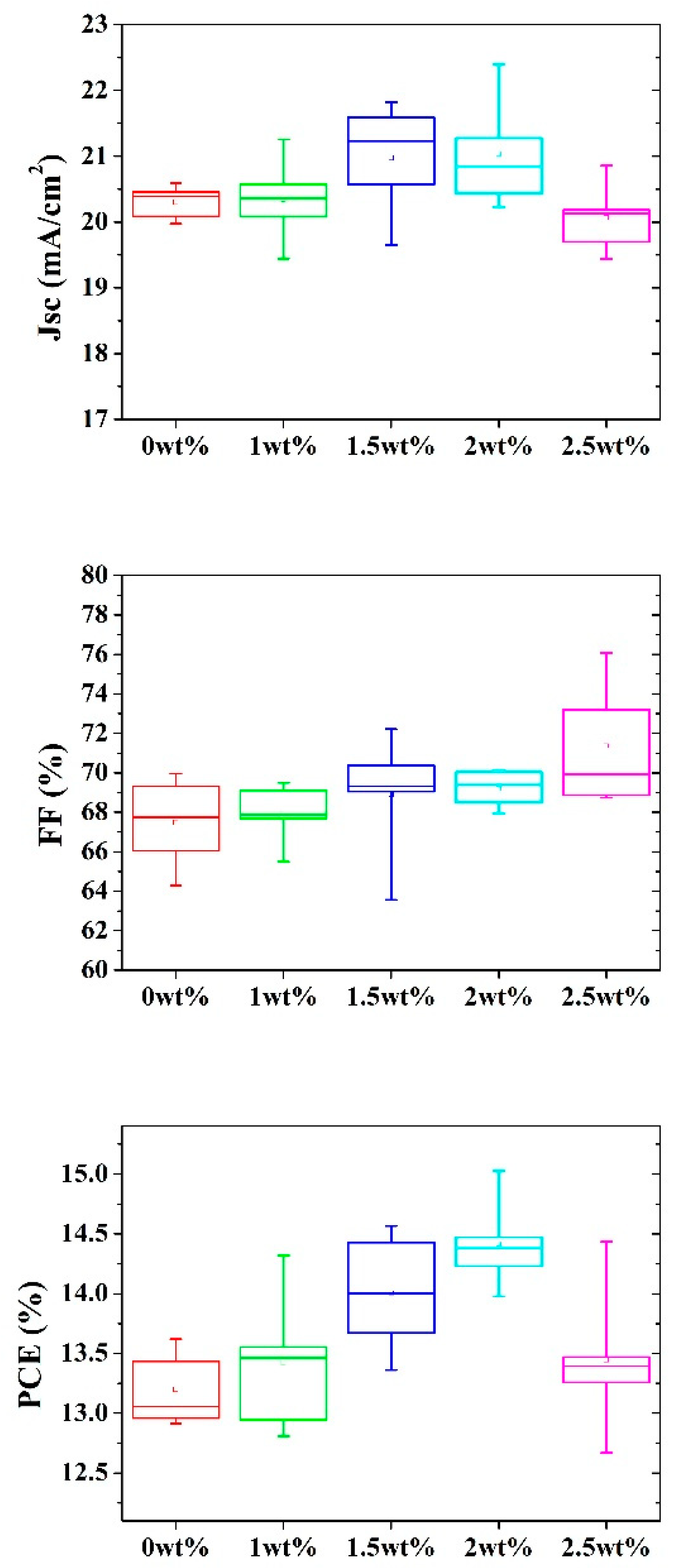
The optimal solvent additive doping rate was obtained by changing the composition ratio of dopant DIO against PEDOT: PSS. Figure 1 shows the change in the open circuit voltage (Voc), short circuit current density (Jsc), fill factor (FF), and power conversion efficiency (PCE) according to the composition ratio of the additive.
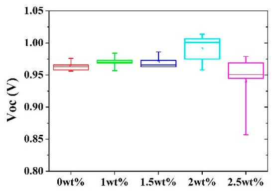
Figure 1.
Device parameters (Voc, Jsc, FF and PCE) as a function of solvent additive (DIO) composition.
The device performances are summarized in Table 1.

Table 1.
Averaged device performances according to DIO doping concentrations.
All of the measured device performances were averaged over at least 10 devices. The best device performance was obtained with a 2 wt% doping ratio and the Voc, Jsc, FF, and PCEs of the PSC at AM 1.5 100 mW/cm2 condition were 0.991 ± 0.024 V, 21.04 ± 0.86 mA/cm2, 0.692 ± 0.010, and 14.42 ± 0.39%, respectively. Since the best device performance was obtained with a 2 wt% doping condition, all the other studies were processed using this doping ratio. The PCE of the device fabricated on the un-doped PEDOT: PSS layer with conventional thermal annealing was 13.20 ± 0.31. Therefore, it can be concluded that doped PEDOT: PSS hole-transporting layer increased the PCE of the device by about 10%.
To find out the electrostatic effect of a dopant (i.e., the surface ion density of the hole-transporting layer) on device performances, the solvent additive DIO was changed to 1,8-dichlorooctane (DCO). Since the electronegativity of chlorine atoms (3.16) is higher than that of iodine atoms (2.66), Pb2+ ions included in perovskite crystal should be more strongly held through electrostatic interaction between chlorine atoms and lead ions. The devices were prepared using the same method as for DIO; however, due to the molecular weight differences between iodide and chlorine (the molecular weight of DCO is 183.12 g/mol, while that for DIO is 366.02 g/mol) the same dopant mole ratio to PEDOT: PSS was reduced to 1 wt%. Table 2 summarizes the device performances with DCO as a dopant. Once again, the device doped with 1 wt% DCO showed the best device performances.
Table 2.
Averaged device performances according to DCO doping concentrations.
The Voc, Jsc, FF, and PCE of PSCs at the AM 1.5 100 mW/cm2 condition were 1.027 ± 0.008 V, 20.68 ± 0.62 mA/cm2, 0.673 ± 0.038, and 14.27 ± 0.52%, respectively. The PCEs of the devices doped with DIO and DCO were within the experimental error range, so it could be concluded that the electrostatic effect of the dopant on the device performance was very weak.
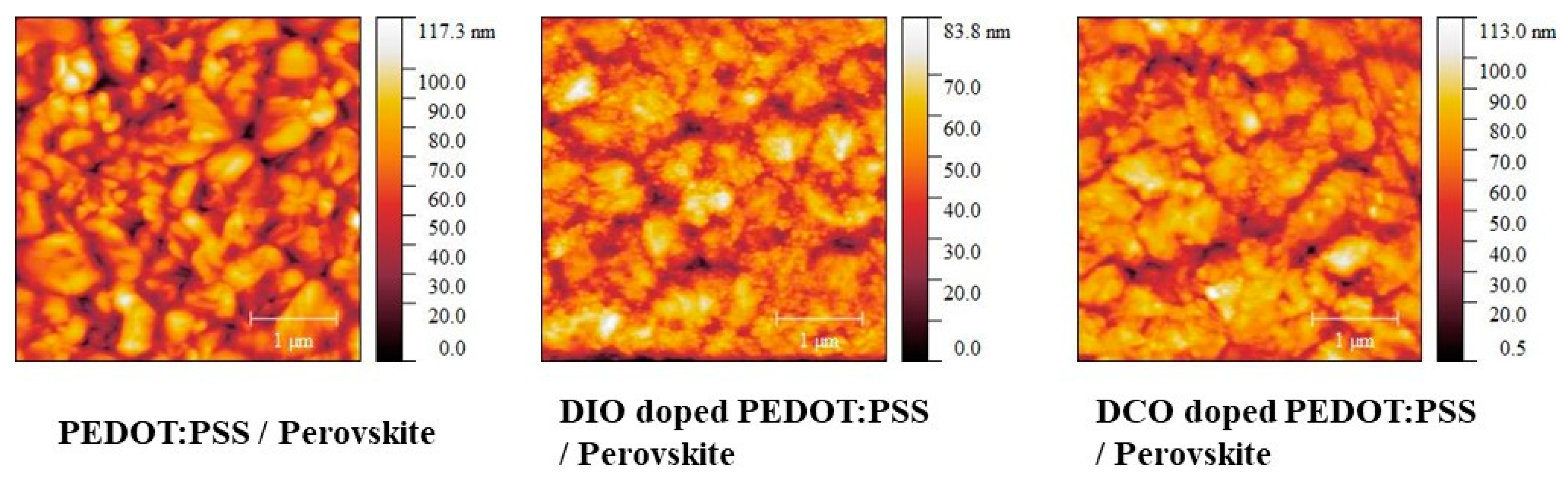
The surface roughness effect on the device performances was tested by preparing three different hole-transporting layers (un-doped PEDOT: PSS film, DIO-doped PEDOT: PSS film, and DCO-doped PEDOT: PSS film). Perovskite film was fabricated on these hole-transporting layers by the one-step method explained in the “Experiment” section. Figure 2 shows AFM topology images of the perovskite grain fabricated on these hole-transporting layers.
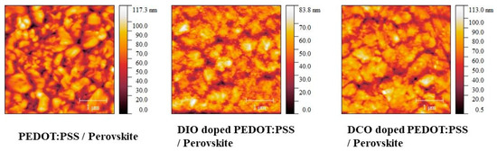
Figure 2.
AFM topology images of the perovskite grain fabricated on three different hole-transporting layers.
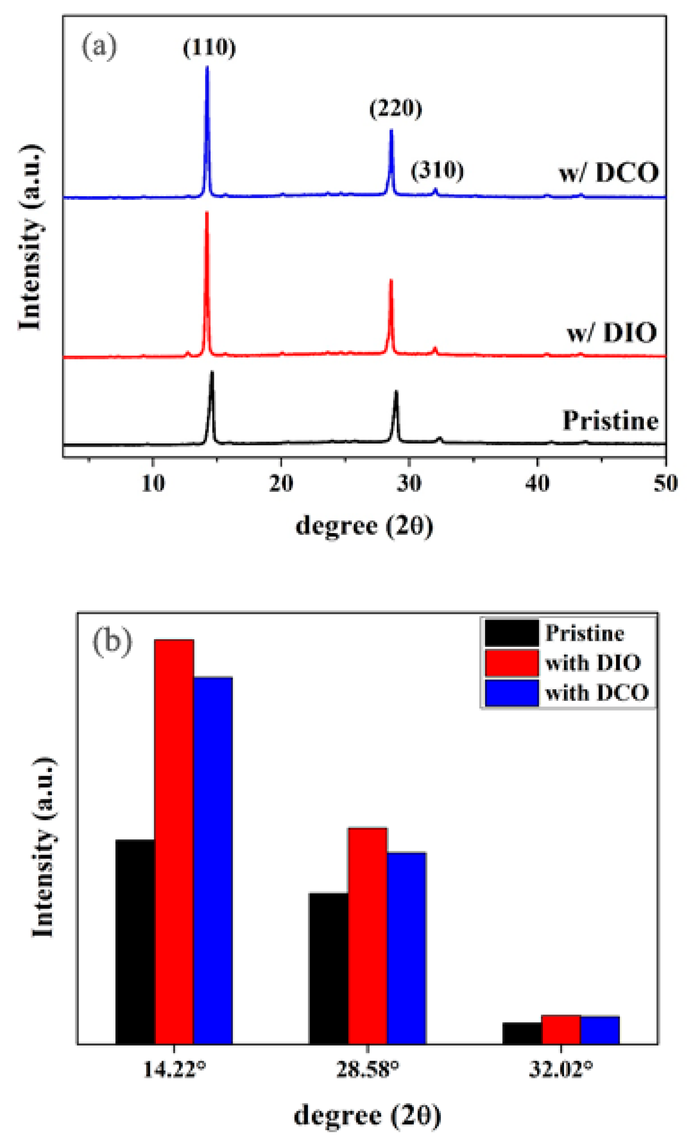
The rms (root mean square) roughness values were 17.15 nm, 10.83 nm and 13.59 nm, respectively. The surface roughness was lowest for the perovskite film coated on the DIO-doped PEDOT: PSS layer. Since the perovskite film was formed on the PEDOT: PSS layer, it was concluded that the smoother the PEDOT: PSS film was the smoother the perovskite film also was. To study the effect of doping on perovskite crystallinity, X-ray diffraction (XRD) analysis was proceeded with. Figure 3 shows the XRD images of the film formed on the three different hole-transporting layers.

Figure 3.
(a) XRD images for the three different hole-transporting layers and (b) the plane diffraction peak intensity ratio of each layer.
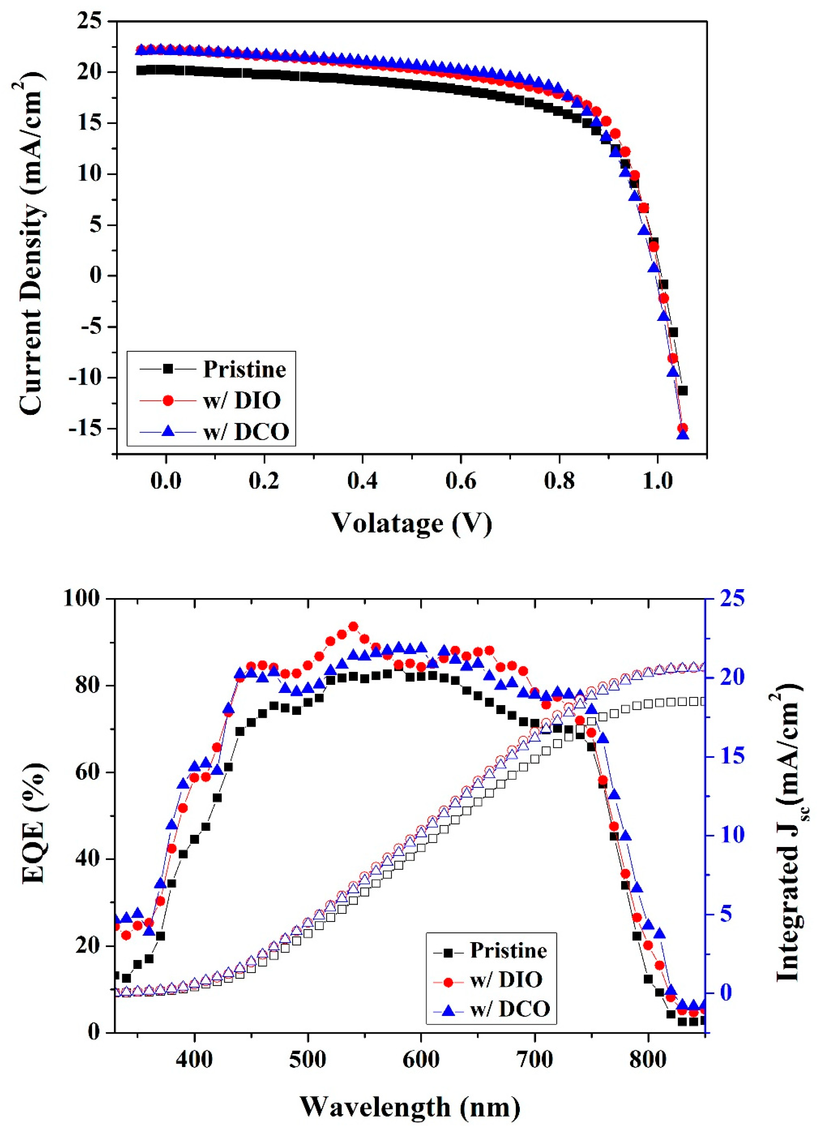
Diffraction peaks appeared at 2θ = 14, 28, and 32°, which assign to the (110), (220), and (310) planes of the tetragonal CH3NH3PbI3 perovskite structures [23]. Compared with XRD peak intensity, it was clear that the crystallinity of perovskite films formed on the doped hole-transporting films (both DIO and DCO) were higher. The surface roughness effect on the device performances was studied by forming devices on these three different hole-transporting layers. The external quantum efficiency (EQE) measurement, as shown in Figure 4, confirms the higher photon absorption in the range of 350–800 nm for the PSCs with additives compared with that for the PSCs without additives.
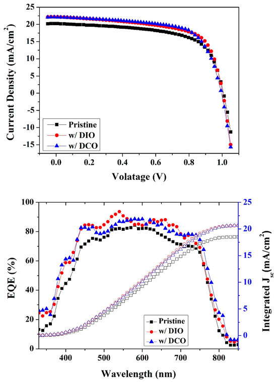
Figure 4.
J-V curves and external quantum efficiency of the devices.
The integral current density of the EQE spectra over the AM 1.5G solar emission spectrum shows values over 20 mA/cm2 for the device with additives and about 18 mA/cm2 for the device without additives. The trend of EQE spectra was consistent with the results of the I-V curve. The PCE of the device formed on the doped hole-transporting films (both DIO and DCO) showed about 10% enhanced efficiency compared with that formed on un-doped hole-transporting films (Table 1 and Table 2). This increase is exactly the same amount as that of the increase in the PCE through the surface smoothness effect due to doping the PEDOT: PSS layer and it confirmed that there was no electrostatic effect contribution.
To analyze the doping effect on the conductivity of the PEDOT: PSS layer, the sheet resistance was measured using four probe methods [24]. The sheet resistances of un-doped PEDOT: PSS film, DIO-doped PEDOT: PSS film, DCO-doped PEDOT: PSS film coated on ITO glass were 181.8, 161.4, and 163.6 Ω, respectively. The thickness of the film that was required to obtain this sheet resistance was measured using SEM, which turned out to be 30.6 nm. The final conductivity of un-doped PEDOT: PSS film, DIO-doped PEDOT: PSS film, DCO doped PEDOT: PSS film were 1796, 2023, 1996 S/cm, respectively. The solvent additive doping of PEDOT: PSS increased the conductivity of PEDOT: PSS film. The conductivity of both DIO- and DCO-doped PEDOT: PSS film was within the experimental error range, so it could be concluded that the conductivity of these doped PEDOT: PSS films was same. Combining these electrostatic surface roughness and conductivity results, device performance enhancement was mainly caused by smoother surface formation and the conductivity increase through doping the HTL.
Enhancement in the conductivity of PEDOT: PSS film was also proved by the increase in the charge transfer rate of the perovskite crystal to PRDOT: PSS. To evaluate the charge transfer from the perovskite layer to PEDOT: PSS film, fluorescence emission intensity was measured using a structure of ITO/PEDOT: PSS (with or without the solvent additive)/perovskite sample. As shown in Figure 5, a greater extent of fluorescence emission quenching (i.e., emission intensity decrease) was observed in the sample with DIO (device with microwave annealing showed higher emission quenching), indicating that the sample with the DIO additive exhibited a slightly higher quenching efficiency of excited states and a better hole transport ability than the device with bare PEDOT:PSS.
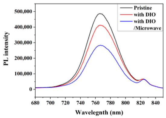
Figure 5.
Fluorescence emission spectra of the perovskite films deposited on bare PEDOT: PSS and DIO-doped PEDOT:PSS.
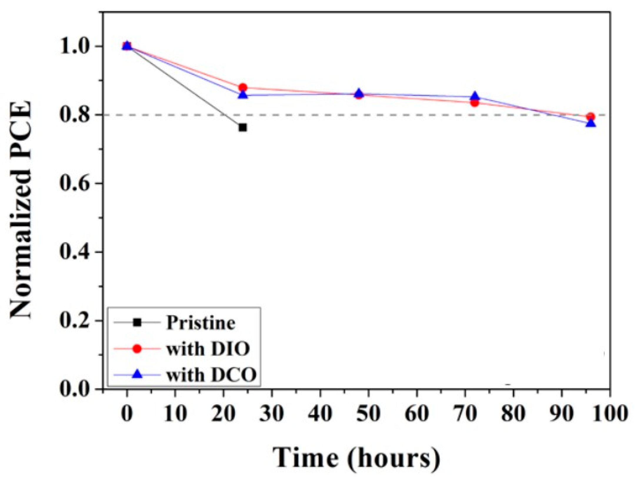
Stability of the devices was tested using un-doped, DIO-doped, and DCO-doped PEDOT: PSS films by measuring the time required for the PCE to fall below 80% of the initial value (LT80). The PCE measurements were proceeded with at room temperature under ambient air conditions without device encapsulation. Figure 6 shows the PCE changes with time for these devices.
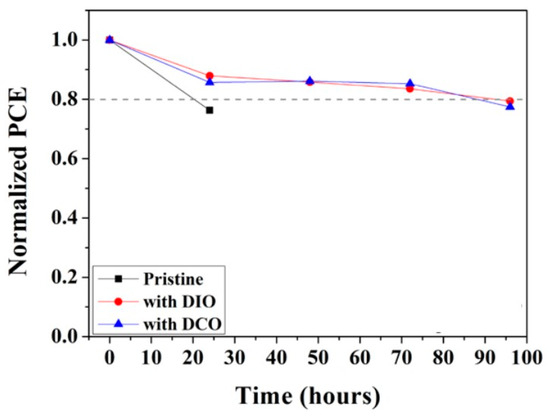
Figure 6.
PCE changes of the devices with un-doped, DIO-doped, and DCO-doped PEDOT: PSS films as a function of time at 35% relative humidity condition without encapsulation.
The device with un-doped PEDOT: PSS film showed the LT80 of 20 h, while devices with both DIO- and DCO-doped PEDOT: PSS film showed the LT80 of about 90 h, which increased by 4.5 times compared with pristine device with un-doped PEDOT: PSS film. This enhancement in device stability resulted from the passivation effect of the bottom of the perovskite due to the additive alkyl di-halides [14]. DIO showed a slightly better LT80 between doping with DIO and DCO; the XRD intensity and AFM roughness values were also slightly better for DIO-doped devices, so all devices were prepared with DIO doping.
When PEDOT: PSS nanoparticles are dispersed in distilled water, it takes a long time to anneal this spin-coated PEDOT: PSS hole-transporting layer (usually more than 10 min), which is another obstacle to the use of mass production methods such as roll-to-roll processing. A microwave annealing process was proceeded with using home-made power adjustable microwave equipment and compared with the conventional thermal annealing. The power of the microwave was set at 200 W (power of general microwave ovens is usually 800~1000 W) and the PEDOT: PSS film was annealed for 10 s, with a rest of 10 s, and annealed for another 10 s. The overall time required for microwave annealing was only 30 s, which is far less than that required for the conventional thermal annealing (typically 15 min in 120 °C oven). Table 3 summarizes the device performances according to annealing conditions.
Table 3.
Device performances according to the annealing method.
The PCE of the device fabricated on the un-doped PEDOT: PSS film with conventional thermal annealing was 13.20 ± 0.31. While that for devices on 2 wt% DIO-doped PEDOT: PSS film was 14.42 ± 0.39% for thermal annealing and 14.44 ± 0.54 for microwave annealing. Doping HTLs increased the PCE of the device by about 10%. When comparing annealing conditions between the microwave and thermal annealing, all device parameters (i.e., Voc, Jsc, FF, and PCE) were quite similar; therefore, it could be concluded that microwave annealing could provide the same device performance while reducing the processing time by 1/30th compared with thermal annealing.
The effect of post-annealing was studied using a very weak power microwave. The conventional microwave power is too strong to the point that it cannot be used for fully fabricated devices (i.e., devices with metal electrodes) because of the reflection from the surface of the metal. In this post-annealing study, the power of the microwave was set at 50 W to penetrate through the metal electrode and to vaporize any trace of moisture contained inside of the device during the fabrication processes. The fully fabricated devices were exposed to microwaves for only 5 s. The PCE was measured before and after microwave treatment. The fabricated devices were stored at an ambient condition with a relative humidity of 35% without device encapsulation. Table 4 summarizes the PCE changes as a function of time.
Table 4.
The PCE change according to post-annealing treatment.
Both un-doped and doped devices showed enhanced PCE after microwave treatment. The un-doped device failed one day after fabrication, while the DIO-doped device survived for 5 days and showed enhanced PCE after microwave treatment. From these results, it could be concluded that a low power microwave treatment could vaporize traces of moisture and prolong the lifetime of the device.
To more effectively check the effect of doping on increasing the stability and lifetime of the devices, the active area was doubled in width and length. The area of the cell was increased from 0.09 cm2 to 0.36 cm2. Table 5 summarizes the best PCE of small and large-area device with different conditions.
Table 5.
Small and large-area devices’ best performances according to different annealing methods.
The PCE of thermally annealed un-doped cells with an area of 0.09 cm2 was 13.62%, while that of such cells with an area of 0.36 cm2 was 9.96%. The PCE of thermally annealed 2 wt% DIO-doped cells with an area of 0.09 cm2 was 15.03%, while that of such cells with an area of 0.36 cm2 was 12.15%. The PCE of a larger area cell was reduced less (about a 27% reduction for un-doped cell sand about a 19% reduction for un-doped cell) for DIO-doped cells, probably due to the better areal uniformity caused by a smoother hole-transporting layer through doping the PEDOT: PSS layer. The PCE of microwave annealed 2 wt% DIO-doped cells with an area of 0.09 cm2 was 14.96%, while that of such cells with an area of 0.36 cm2 was 12.21%. The PCE drop of larger area cells was about 18% for this microwave annealing condition. Once again, the microwave annealing did not affect the device performance even for larger area cells, it could only reduce the time required for annealing to 1/30th compared with that of thermal annealing.
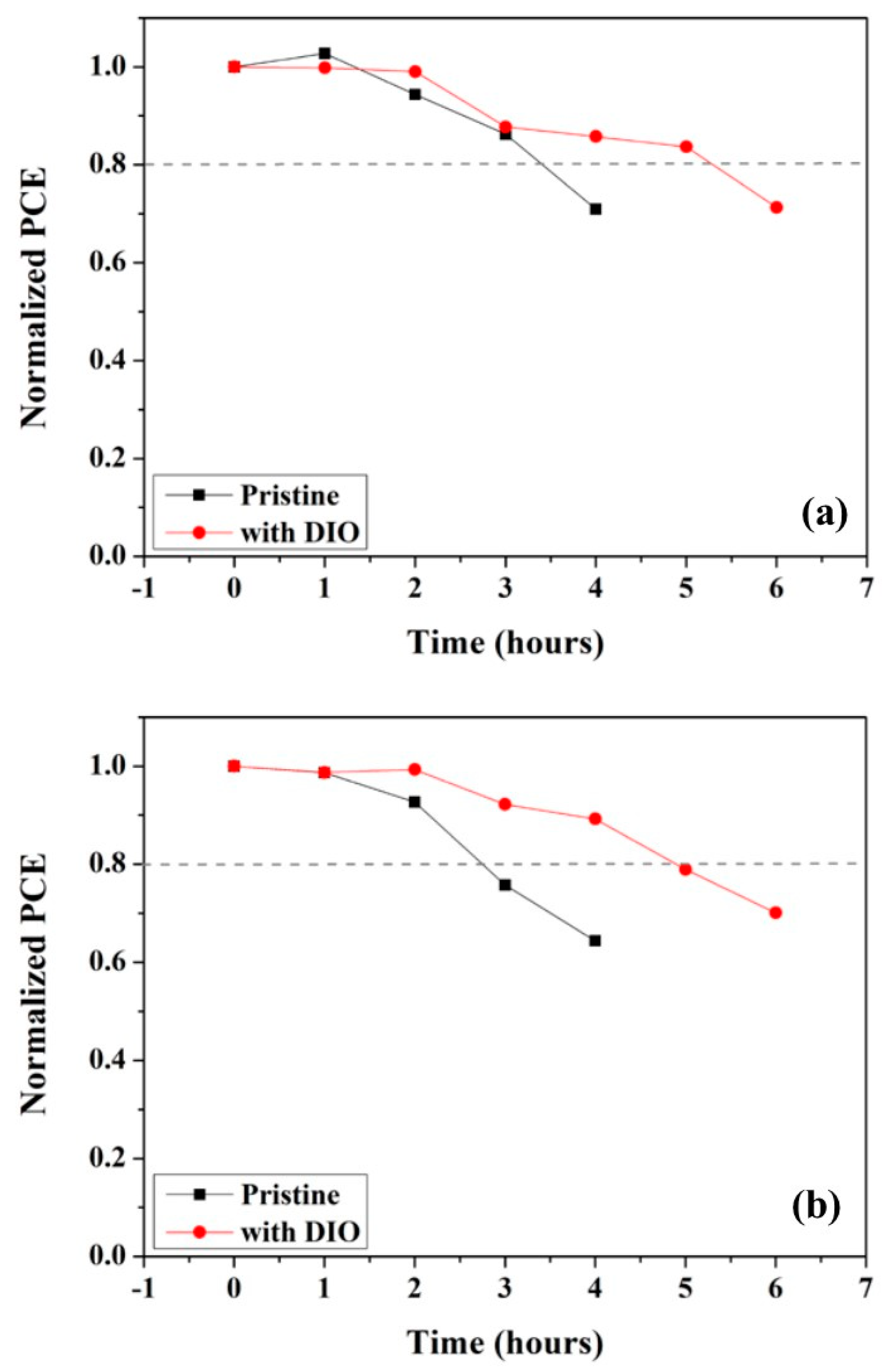
Long-term stability of the larger area device was also studied. The time required for LT80 conditions was measured while the devices were exposure to 100 mW/cm2 of solar simulator light at a relative humidity of 35% without device encapsulation (Figure 7a,b). Figure 7a shows the 0.09 cm2 cell data whereby the LT80 for an un-doped cell was 3.4 h and that for a 2 wt% DIO-doped cell was 5.3 h. The lifetime of doped devices was enhanced by about 1.6 times compared with that for un-doped devices. Figure 7b shows the 0.36 cm2 cell data whereby the LT80 for an un-doped cell was 2.7 h and that for a 2 wt% DIO-doped cell was 4.9 h. The lifetime of doped, larger-size devices was enhanced by about 1.8 times compare to that for un-doped devices. Even though the absolute value of the LT80 for larger-size cell decreased as the cell area increased (i.e., in the case of doped cells, 5.3 h for 0.09 cm2 cell and 4.9 h for the 0.36 cm2 cell), as the size of the cell increased the extent of the lifetime enhancement through doping increased (i.e., 1.6 times for the 0.09 cm2 cell and 1.8 times for the 0.36 cm2 cell). Since the device lifetime was very short when the device was exposed to solar simulator light without encapsulation and to mimic a more realistic situation, the device storage method was changed. The devices were stored at a relative humidity of 35% without device encapsulation; however, Figure 7c,d show the PCE changes as a function of time for the devices stored in scattered light (Figure 7c) and in the dark (Figure 7d). Figure 7c shows the PCE changes for the 0.09 cm2 cell data; LT80s were dramatically increased compared with the devices exposed to the illumination with the same device area (i.e., Figure 7a).
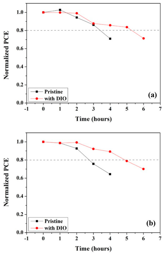
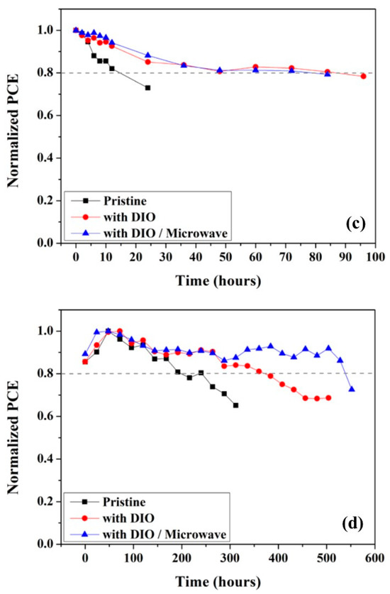
Figure 7.
PCE changes as a function of time to obtain LT80. (a) The 0.09 cm2 cell exposure to 100 mW/cm2 solar simulator light at a relative humidity of 35% without encapsulation, (b) the 0.36 cm2 cell exposure to 100 mW/cm2 of solar simulator light at a relative humidity of 35% without encapsulation, (c) the 0.09 cm2 cell stored at a relative humidity of 35% without device encapsulation, and (d) the 0.36 cm2 cell stored at a relative humidity of 35% without device encapsulation.
The LT80 for un-doped cell was 15 h and that for 2 wt% DIO-doped cell was 78 h. The lifetime enhancement for doped device was about 5.2 times compare that for un-doped device. Figure 7d shows the PCE changes for 0.36 cm2 cell data, the LT80 for un-doped cell was 192 h and that for 2 wt% DIO-doped cell was 540 h. The lifetime enhancement for doped device was about 2.8 times compare that for un-doped device. From these experiments, it could be concluded that the differences in the lifetime between un-doped and doped devices decreased when the devices were stored at the dark environment.
4. Conclusions
A novel processing technology to improve the stability of PSCs using doping hole-transporting layers was examined. The optimal doping rate was 2 wt% of DIO to PEDOT: PSS and this doping enhanced the PCE of the device by about 10%. The electrostatic effect of the dopant on the device performances was studied by changing the dopant from DIO to DCO. Replacing the atoms in the dopant from diiodide to dichloride changed the ion density of the HTL (because of differences in the electronegativity between chlorine and iodine) and resulted in an electrostatic interaction change between the halide atoms of the dopant and the lead ions of the perovskite crystal. Due to the molecular weight differences between iodide and chlorine, the same dopant mole ratio to PEDOT was reduced to 1 wt% and this composition showed the best device performance. The device performances were within the experimental error range, so it could be concluded that the electrostatic effect was a very weak influence on the device performances.
The surface roughness effect on the device performances was examined using AFM. Doped HTL produced a smoother surface, resulting in a smoother perovskite surface. According to the XRD diffraction peak intensity study, the perovskite crystallinity formed on the doped HTL (both DIO and DCO) was higher. The conductivity of the HTL was measured using a four probe method and was higher for doped devices. Combining these electrostatic, surface roughness, and conductivity results, the enhancement of device performance was mainly caused by smoother surface formation and an increase in conductivity rather than the electrostatic interaction.
Long-term stability of the device was tested by measuring the time required for the PCE to fall below 80% of the initial value. DIO doping appeared to be slightly better than DCO doping on device performance. When a 200 W microwave was used to anneal PEDOT: PSS film, the processing time was reduced to 1/30th of that when thermal annealing was used without losing device performance. A lower power (50 W) microwave treatment was used for the post-annealing of the fully fabricated devices and it turned out to vaporize traces of moisture and prolong the lifetime of the device. Stability enhancement was studied using a larger area cell; the doped devices showed much more enhanced device lifetime compared with that for un-doped devices. According to larger size cell studies, the device lifetime was decreased as the cell area increased; however, as the size of the cell increased, the extent of lifetime enhancement through doping increased. These enhancements of long-term stability were attributed to the passivation process. The partially electro-negative halogen (i.e., Iδ− and Clδ−) in DIO and DCO could interact with the Pb2+ of the perovskite crystal while the hydrophobic aliphatic moiety (i.e., partially positive octyl groups) can passivate the surface of perovskite thin film from moisture. This passivation effect through the surface modification of the perovskite grains could be beneficial for the long-term stability of devices and is well studied [14,25,26,27,28].
Author Contributions
Methodology, M.J.K.; investigation, H.L. and J.Y.J.; writing—review and editing, supervision, funding acquisition, J.-W.Y. All authors have read and agreed to the published version of the manuscript.
Funding
This work was supported by the National Research Foundation of Korea (NRF) with grant funded by the Korean government (MSIT) (Grant No. 2022R1F1A1070498. All solution-processed thin film and encapsulation film for flexible electronics).
Institutional Review Board Statement
Not applicable.
Informed Consent Statement
Not applicable.
Data Availability Statement
Data are contained within the article.
Conflicts of Interest
The authors declare no conflict of interest.
References
- Kojim, A.; Teshima, K.; Shirai, Y.; Miyasaka, T. Organometal Halide Perovskites as Visible-Light Sensitizers for Photovoltaic Cells. J. Am. Chem. Soc. 2009, 131, 6050–6051. [Google Scholar] [CrossRef] [PubMed]
- Best Research-Cell Efficiency Chart, NREL. 2023. Available online: https://www.nrel.gov/pv/cell-efficiency.html (accessed on 20 June 2023).
- Luo, D.; Yang, W.; Wang, Z.; Sadhanala, A.; Hu, Q.; Su, R.; Shivanna, R.; Trindade, G.F.; Watts, J.F.; Xu, Z.; et al. Enhanced photovoltage for inverted planar heterojunction perovskite solar cells. Science 2018, 360, 1442–1446. [Google Scholar] [CrossRef] [PubMed]
- Yip, H.-L.; Jen, A.K.-Y. Recent advances in solution-processed interfacial materials for efficient and stable polymer solar cells. Energy Environ. Sci. 2012, 5, 5994–6611. [Google Scholar] [CrossRef]
- Liu, T.; Chen, K.; Hu, Q.; Zhu, R.; Gong, Q. Inverted perovskite solar cells: Progresses and perspectives. Adv. Energy Mater. 2016, 6, 1600457. [Google Scholar] [CrossRef]
- Hu, Y.; Tang, Y.; Zhang, Z.; Yang, F.; Jiang, L.; Song, Y.; Liu, H. Improving the efficiency of inverted perovskite solar cells by Bis (acetylacetonato) dioxomolybdenum (VI)-doped PEDOT: PSS. Mater. Lett. 2022, 306, 130911. [Google Scholar] [CrossRef]
- Xu, L.; Li, Y.; Zhang, C.; Liu, Y.; Zheng, C.; Lu, W.; Li, M.; Chen, Y.; Huang, W.; Chen, R. Improving the efficiency and stability of inverted perovskite solar cells by CuSCN-doped PEDOT: PSS. Solar Energy Mater. Solar Cells 2020, 206, 110316. [Google Scholar] [CrossRef]
- Liu, D.; Li, Y.; Yuan, J.; Hong, Q.; Shi, G.; Yuan, D.; Wei, J.; Huang, C.; Tang, J.; Fung, M.-K. Improved performance of inverted planar perovskite solar cells with F4-TCNQ doped PEDOT: PSS hole transport layers. J. Mater. Chem. 2017, 5, 5701–5708. [Google Scholar] [CrossRef]
- Niu, J.; Yang, D.; Ren, X.; Yang, Z.; Liu, Y.; Zhu, X.; Zhao, W.; Liu, S. Graphene-oxide doped PEDOT: PSS as a superior hole transport material for high-efficiency perovskite solar cell. Org. Electron. 2017, 48, 165–171. [Google Scholar] [CrossRef]
- Redondo-Obispo, C.; Ripollesa, T.S.; Cortijo-Campos, S.; Álvareza, A.L.; Climent-Pascual, E.; de Andrés, A.; Coya, C. Enhanced stability and efficiency in inverted perovskite solar cells through graphene doping of PEDOT: PSS hole transport layer. Mater. Design 2020, 191, 108587. [Google Scholar] [CrossRef]
- Hu, L.; Sun, K.; Wang, M.; Chen, W.; Yang, B.; Fu, J.; Xiong, Z.; Li, X.; Tang, X.; Zang, Z.; et al. Inverted planar perovskite solar cells with a high fill factor and negligible hysteresis by the dual effect of NaCl-doped PEDOT: PSS. ACS Appl. Mater. Interfac. 2017, 9, 43902–43909. [Google Scholar] [CrossRef]
- Jiang, K.; Wu, F.; Zhang, G.; Chow, P.C.Y.; Ma, C.; Li, S.; Wong, K.S.; Zhu, L.; Yan, H. Inverted planar perovskite solar cells based on CsI-doped PEDOT: PSS with efficiency beyond 20% and small energy loss. J. Mater. Chem. 2019, 7, 21662–21667. [Google Scholar] [CrossRef]
- Huang, P.; Liu, Y.; Zhang, K.; Yuan, L.; Li, D.; Hou, G.; Dong, B.; Zhou, Y.; Song, B.; Li, Y. Catechol derivatives as dopants in PEDOT: PSS to improve the performance of p–i–n perovskite solar cells. J. Mater. Chem. 2017, 5, 24275–24281. [Google Scholar] [CrossRef]
- Zhu, Y.; Wang, S.; Ma, R.; Wang, C. The improvement of inverted perovskite solar cells by the introduction of CTAB into PEDOT: PSS. Solar Energy 2019, 188, 28–34. [Google Scholar] [CrossRef]
- Erazoa, E.A.; Castillo-Bendeck, D.; Ortiz, P.; Cortés, M.T. NaCl doped electrochemical PEDOT: PSS layers for inverted perovskite solar cells with enhanced stability. Synth. Met. 2019, 257, 116178. [Google Scholar] [CrossRef]
- Wang, W.; Qin, F.; Zhu, X.; Liu, Y.; Jiang, X.; Sun, L.; Xie, C.; Zhou, Y. Exploring the Chemical Interaction between Diiodooctane and PEDOT-PSS Electrode for Metal Electrode-Free Nonfullerene Organic Solar Cell. ACS Appl. Mater. Interfaces 2020, 12, 3800–3805. [Google Scholar] [CrossRef] [PubMed]
- Xia, Y.; Dai, S. Review on applications of PEDOTs and PEDOT: PSS in perovskite solar cells. J. Mater. Sci. Mater. Electr. 2021, 32, 12746–12757. [Google Scholar] [CrossRef]
- Wang, Q.; Chueh, C.-C.; Eslamian, M.; Jen, A.K.-Y. Modulation of PEDOT:PSS pH for efficient inverted perovskite solar cells with reduced potential loss and enhanced stability. ACS Appl. Mater. Interfaces 2016, 8, 32068–32076. [Google Scholar] [CrossRef]
- Xue, Q.; Liu, M.; Li, Z.; Yan, L.; Hu, Z.; Zhou, J.; Li, W.; Jiang, X.-F.; Xu, B.; Huang, F.; et al. Efficient and stable perovskite solar cells via dual functionalization of dopamine semiquinone radical with improved trap passivation capabilities. Adv. Funct. Mater. 2018, 28, 1707444. [Google Scholar] [CrossRef]
- Yang, L.; Cai, F.; Yan, Y.; Li, J.; Liu, D.; Pearson, A.J.; Wang, T. Conjugated small molecule for efficient hole transport in high-performance p-i-n type perovskite solar cells. Adv. Funct. Mater. 2017, 27, 1702613. [Google Scholar] [CrossRef]
- Kim, J.H.; Williams, S.T.; Cho, N.; Chueh, C.-C.; Jen, A.K.-Y. Enhanced Environmental Stability of Planar Heterojunction Perovskite Solar Cells Based on Blade-Coating. Adv. Energy Mater. 2015, 5, 1401229. [Google Scholar] [CrossRef]
- Liang, P.-W.; Liao, C.-Y.; Chueh, C.-C.; Zuo, F.; Williams, S.T.; Xin, X.-K.; Lin, J.; Jen, A.K.-Y. Additive enhanced crystallization of solution-processed perovskite for highly efficient planar-heterojunction solar cells. Adv. Mater. 2014, 26, 3748–3754. [Google Scholar] [CrossRef] [PubMed]
- Zhao, Y.; Zhu, K. Optical Bleaching of Perovskite (CH3NH3)PbI3 Through Room-Temperature Phase Transformation Induced by Ammonia. Chem. Commun. 2014, 50, 1605–1607. [Google Scholar] [CrossRef] [PubMed]
- Miccoli, I.; Edler, F.; Pfnür, H.; Tegenkamp, C. The 100th anniversary of the four-point probe technique: The role of probe geometries in isotropic and anisotropic systems. J. Phys. Condens. Matter 2015, 27, 223201. [Google Scholar] [CrossRef] [PubMed]
- Zuo, L.; Guo, H.; deQuilettes, D.W.; Jariwala, S.; De Marco, N.; Dong, S.; DeBlock, R.; Ginger, D.S.; Dunn, B.; Wang, M.; et al. Polymer-modified halide perovskite films for efficient and stable planar heterojunction solar cells. Sci. Adv. 2017, 3, e1700106. [Google Scholar] [CrossRef]
- Terry, M.L.; Straub, A.; Inns, D.; Song, D.; Aberle, A.G. Large open-circuit voltage improvement by rapid thermal annealing of evaporated solid-phase-crystallized thin-film silicon solar cells on glass. Appl. Phys. Lett. 2005, 86, 172108. [Google Scholar] [CrossRef]
- Li, X.; Dar, M.I.; Yi, C.; Luo, J.; Tschumi, M.; Zakeeruddin, S.M.; Nazeeruddin, M.K.; Han, H.; Grätzel, M. Improved performance and stability of perovskite solar cells by crystal crosslinking with alkylphosphonic acid ω-ammonium chlorides. Nat. Chem. 2015, 7, 703–711. [Google Scholar] [CrossRef]
- Wang, Y.; Zhang, T.; Kan, M.; Zhao, Y. Bifunctional Stabilization of All-Inorganic α-CsPbI3 Perovskite for 17% Efficiency Photovoltaics. J. Am. Chem. Soc. 2018, 140, 12345–12348. [Google Scholar] [CrossRef]


Disclaimer/Publisher’s Note: The statements, opinions and data contained in all publications are solely those of the individual author(s) and contributor(s) and not of MDPI and/or the editor(s). MDPI and/or the editor(s) disclaim responsibility for any injury to people or property resulting from any ideas, methods, instructions or products referred to in the content. |
© 2023 by the authors. Licensee MDPI, Basel, Switzerland. This article is an open access article distributed under the terms and conditions of the Creative Commons Attribution (CC BY) license (https://creativecommons.org/licenses/by/4.0/).