Abstract
Plasmonic sensors have great potential for widespread usage. However, the prohibitive cost of noble metals restrains the wider adoption of these devices. The aim of our study is to develop a cost-effective Al-based alternative to common noble metal-based plasmonic detectors. We considered a structure consisting of an n-type doped Si wafer with a shallow p-n junction and an overlying Al grating with a trapezoidal groove profile. The RCWA (rigorous coupled-wave analysis) method was used to numerically calculate the distribution of absorbed light energy in the plasmonic detector layers and to optimize the grating parameters. Based on the simulation results, experimental samples of plasmonic photodetectors with optimal grating parameters (period—633 nm, relief depth—50 nm, groove filling factor—0.36, and thickness of the intermediate Al layer—14 nm) were manufactured, and their properties were studied. For these samples, we obtained a polarization sensitivity value of Ip/Is = 8, an FWHM of the resonance in the photocurrent spectrum ranging from 50 to 100 nm, a sensitivity at the resonance maximum of Iph = 0.04–0.06 A/W, and an angular half-width of photocurrent resonance of Δθ = 5°, which are comparable to noble metal-based analogs. Our results may be used for creating cost-effective high-sensitivity plasmonic sensors.
1. Introduction
Surface plasmon–polaritons (SPPs) are electromagnetic surface waves that propagate along the boundary between a metal and a dielectric or semiconductor, with the maximum field located at this interface and decaying exponentially in both media [1]. Being a non-radiative mode, such a surface wave requires matching its wave vector with the wave vector of the incident light, which, in most cases, is accomplished using a coupling prism [2,3,4] or diffraction grating [5,6,7]. Under optimal conditions, the complete transformation of light energy into the energy of surface plasmon–polaritons is achieved, accompanied by a local increase in the intensity of the electromagnetic field at the interface with the metal plasmon-carrying film. Such spatial localization of the electromagnetic field at the incident photon energy greater than the band gap of the semiconductor contributes to an increase in the generation of electron–hole pairs in it near the contact with the metal and a corresponding increase in the photocurrent in the presence of a built-in electric field separating the charge carriers. At energies lower than the band gap, the excitation of hot electrons in the metal film with subsequent ballistic transport to the semiconductor region with the built-in electric field is possible [8,9,10,11]. Thus, the spectral sensitivity range of such photodetectors can extend beyond the band-to-band generation region by expanding into the red spectral region. Based on this phenomenon, the design of a so-called plasmon–polariton photodetector (PPPD) was proposed [8,12,13]. To excite SPPs in such detectors, a periodically textured semiconductor surface (diffraction grating) with a thin layer of plasmonic metal deposited on it is used. GaAs, Si, and InP were proposed as semiconductors, and films of the noble metals Au and Ag, as well as Al films, were used as plasmon-carrying metals [14,15]. The application area of such photodetectors is quite wide: they are used in sensing, photovoltaics, telecommunications, etc. [14,15,16,17,18]. The basic principle underlying the devices’ operation is the resonant enhancement of the short-circuit photocurrent generated under surface plasmon resonance (SPR) conditions in a Schottky junction at the metal-semiconductor contact [8,19]. However, the presence of a corrugated interface at the Schottky junction contributes to enhanced carrier recombination and scattering, leading to the attenuation of the useful signal. In this regard, PPPD designs with a flat metal-semiconductor interface have been proposed, with the grating relief formed on the outer side of the plasmon-carrying metallic film [20].
For PPPDs based on n-type doped silicon, a scheme with a shallow p-n junction and a distance of about 100 nm from the plasmon-carrying metal layer to the p-n junction has been proposed [21]. This approach eliminates the need to form a high Schottky barrier at the metal–semiconductor interface, which is not always possible for Au/Si or Al/Si pairs. In this case, the separation of photo-carriers occurs in the p-n junction region, i.e., remote from the metal/Si interface, which is characterized by a high surface recombination rate. The influence of deep levels formed by Au in Si on the increase in recombination is also reduced. Moreover, the metal/Si interface can remain flat, simplifying the manufacturing process.
Most studies on PPPDs have been carried out on structures comprising noble metals, mainly gold. Gold has slightly worse plasmonic characteristics (in particular, the ratio of the real and imaginary parts of the dielectric constant) than silver, but it is much more resistant to degradation during operation. It was shown in [18,22] that cheaper aluminum has plasmonic characteristics even better than gold in a significant spectral range, especially in the blue and ultraviolet parts of the spectrum. At the same time, aluminum films are naturally oxidized in air at room temperature to form a relatively stable Al2O3 dielectric layer, which protects the plasmon-carrying metal layer from degradation. However, in the red and infrared spectral regions, the plasmonic characteristics of aluminum are significantly inferior to those of gold; therefore, most SPP sensors (including PPPDs) currently use gold as a plasmon-carrying metal. But research and development related to the use of Al in plasmonics are expanding, and the number of publications on this topic has been growing rapidly recently [23,24]. The possibility of using Al gratings in SPR sensors, [25] and polarization-sensitive detectors [17] and for enhancing up-conversion photoluminescence [26] has been shown. However, detailed studies of aluminum plasmonic detectors based on silicon p-n junctions that include modeling and optimization of the parameters of such structures, have not been carried out yet.
The performance of PPPDs based on aluminum may be optimized for specific applications by choosing optimal grating geometric characteristics. In this work, the parameters of PPPDs based on silicon p-n junctions and aluminum as the plasmon-carrying metal were optimized. An optical smoke detector was selected as a device that uses the PPPD under study as an optical sensor. The most affordable on the market laser with a wavelength of 808 nm is the light source in such a device. Using the RCWA method [27,28], theoretical simulations of the electromagnetic field intensity distribution in the proposed PPPD structure were carried out, and optimal characteristics of the plasmon-carrying layer grating were selected. Experimental samples of PPPDs with optimal aluminum gratings were fabricated, and their characteristics were investigated. It is shown that the polarization sensitivity of these samples is comparable to that obtained for PPPDs with gold films. The proposed PPPD design includes only Al, Cr, Si, and Ti, thus significantly reducing production costs.
2. Materials and Methods
2.1. Fabrication of PPPDs on Si Substrates
For fabricating PPPDs, a pre-made p-n junction on n-Si (111) with a burial depth of 100 nm and 25/250 nm Ti/Ni ohmic rear contacts were used. The necessary periodic relief structures (gratings) on the silicon surface were created using interference lithography with thermally deposited chalcogenide photoresists in a vacuum [20]. A particular feature of this technology, compared to the standard one where the grating is etched into the semiconductor, is the profiling of the metallic plasmon-carrying Al film only. This maintains a flat metal/semiconductor interface with low recombination of the photo-generated carriers. Such a PPPD has a simpler construction and good resonant properties [20].
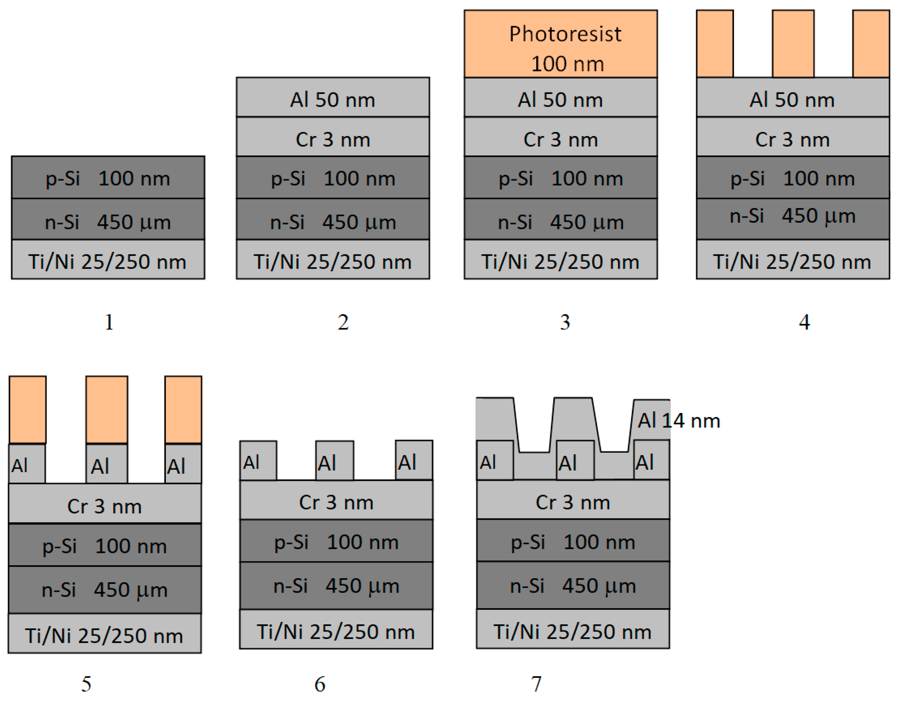
A schematic representation of the step-by-step (1–7) process of fabricating Al gratings on a Si surface is shown in Figure 1. Before installation into the vacuum chamber, the working side of the Si wafer was cleaned in ethyl alcohol and a 5% aqueous solution of HF, followed by rinsing with distilled water and drying with compressed air (Figure 1, 1). The subsequent steps involved the sequential vacuum thermal deposition of an adhesive Cr layer with a mass thickness of ~3 nm and an Al layer of optimal thickness onto the Si surface (Figure 1, 2). This thickness determined the depth of modulation of the surface relief, D. After cooling the wafer to room temperature, a layer of chalcogenide photoresist As40S40Se20 with a thickness of ~100 nm was deposited on the Al surface (Figure 1, 3). The photoresist was exposed in the interference zone of two coherent laser beams emitted by a helium–cadmium laser (wavelength λ = 441.6 nm). The spatial period of the light intensity distribution in the interference zone depended on the convergence angle of the beams and determined the grating period, a. After exposure, the photoresist was selectively etched to form a mask, which allowed access of the etchant to the open areas of the Al layer (Figure 1, 4).
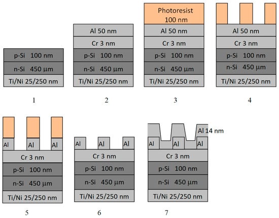
Figure 1.
Key stages of manufacturing a PPPD using aluminum as the plasmon-carrying metal.
The selective etchant used for the photoresist As40S40Se20 contained ethylenediamine (C2H8N2) as an active substance and dimethylsulfoxide (C2H6OS) and acetone (C3H6O) as solvents at a ratio of 2:55:43. At the optimal etchant temperature (20–25 °C), the etching process took about 3 min. After creating the relief lithographic mask, the Al layer in the mask openings was removed using an etchant based on orthophosphoric (H3PO4) and acetic (H3COOH) acids, and distilled water at a ratio of 6:2:2 (Figure 1, 5). The final steps of forming the relief structure of the PPPD involved removing the lithographic mask (Figure 1, 6) and the vacuum thermal deposition of an additional Al layer of thickness d onto the obtained relief (Figure 1, 7). The etchant used for removing the photoresist mask contained ethylenediamine (C2H8N2) and dimethylsulfoxide (C2H6OS) at a ratio of ~1:9. The aluminum grating on the silicon wafer surface provided the excitation of SPR and also served as the upper electrical contact.
2.2. Morphological Characterization
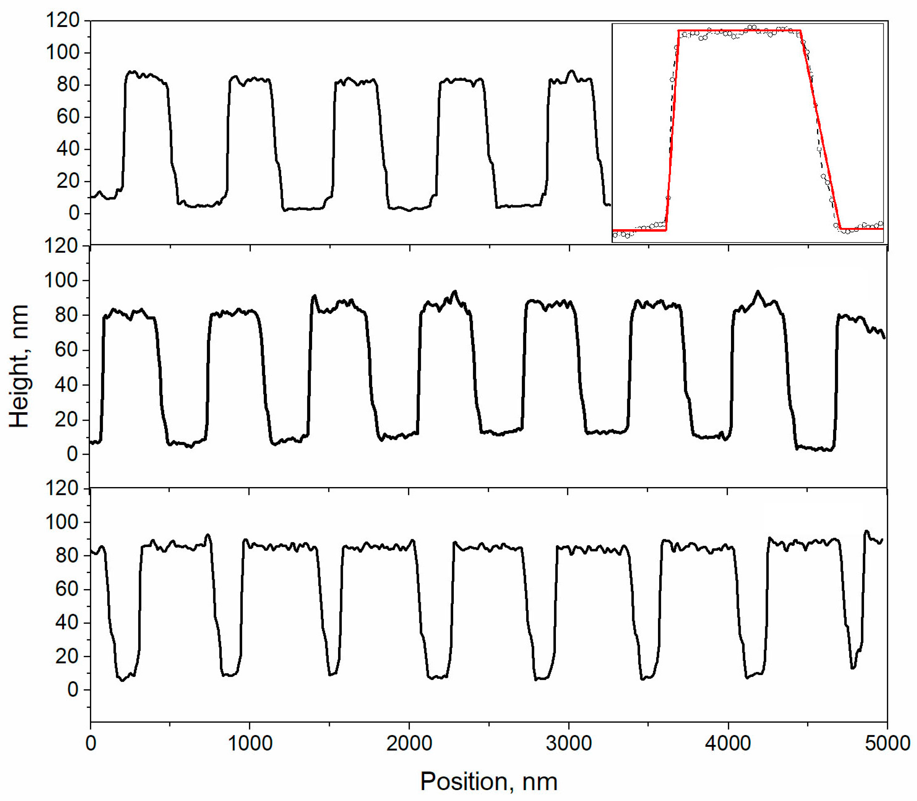
The surfaces of the gratings were morphologically characterized using a Dimension 3000 Scanning Probe atomic force microscope (Digital Instruments Inc., Tonawanda, NY, USA) in the tapping mode. When determining the profile shape of grating grooves using a profilometer or AFM [29], the ratio between the curvature radius of the probe tip and the period and depth of the groove is of great importance. The smaller the grating period is and the greater the depth of its grooves, the greater the deviation of the probe trajectory during the scanning of the sample relief from the real groove profile [29]. In our case, the curvature radius of the probe tip was 7 nm, two orders of magnitude smaller than the grating period (633 nm). Moreover, the gratings were rather shallow: the relief depth was less than 12% of the period, and the minimal slope of the groove side sections relative to the normal to substrate plane was more than 30°. At the same time, the cone angle of the probe tip used by us was 22°. Thus, these factors do not affect our profilometry results. Figure 2 shows a cross-section of the surface microrelief of several manufactured PPPDs with a plane perpendicular to the Al grating grooves.
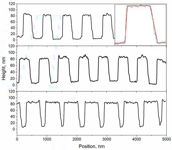
Figure 2.
AFM cross-sections of the Al gratings on the surface of the Si wafer. The inset shows the grating groove profile and its approximation with a trapezoid.
It can be seen (see inset in Figure 2) that the cross-sectional shape of the grating grooves is close to a trapezoid with a varying filling factor (i.e., the ratio of the groove width to the grating period). The parameters of the trapezoid and filling factor were determined by the parameters of the interference lithography process: exposure time, etching time, characteristics of the resist, selective etchant, and etchant for removing the photoresist mask. By varying these parameters, the characteristics of the grating were optimized in accordance with the results of numerical modeling, which are presented in the following section of this article.
2.3. Optical Characterization
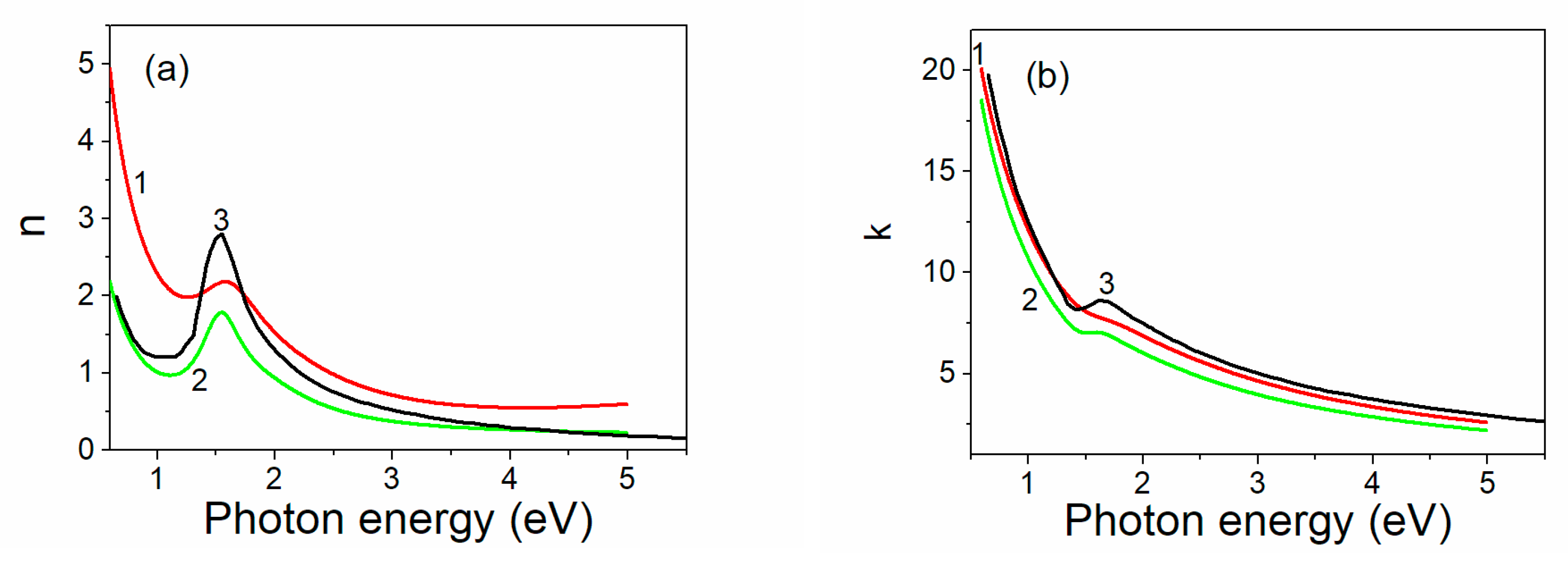
The optical constants of the thin aluminum films deposited on substrates by vacuum thermal evaporation were measured in the spectral range of 250–2100 nm using a SE-2000 (Semilab Ltd., Budapest, Hungary) spectroscopic ellipsometer. Figure 3a,b present the spectral dependencies of the refractive index n and extinction coefficient k for the Al films without thermal annealing after sputtering. As can be seen in the figures, the optical constants of the thin films somewhat differ from the literature data, which typically correspond to bulk materials. This difference is primarily due to enhanced electron scattering at the film boundaries and spatial confinement effects. It is crucial to consider this phenomenon when modeling the resonant properties of PPPDs to ensure accurate predictions and optimized device performance.
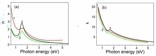
Figure 3.
Spectral dependences of (a) refractive index n and (b) extinction coefficient k for 15 nm (Curve 1) and 50 nm (Curve 2) thick Al films. Curve 3—literature data [30] for bulk material.
The spectral and angular dependences of the short-circuit photocurrent Iph of the manufactured PPPD samples in the wavelength range of 0.4–1.1 μm were also studied under illumination with p- and s-polarized light at incidence angles of θ = 0–70°. The measuring setup included a tungsten lamp light source (Ocean Insight, Rochester, NY, USA), a light chopper (MD Helicopters, Mesa, AZ, USA), a monochromator (Instrument Design Technology Ltd., Widnes, UK), a polarizer of the Glan prism type (Thorlabs, Inc., Newton, NJ, USA), a photodetector with an amplifier (Thorlabs, Inc., Newton, NJ, USA), a rotating sample holder (ICE Oxford Ltd., Witney, UK), and a controller computer (JHC Technology, Taipei City, Taiwan) [31].
3. Simulation of the Proposed Structure and Parameter Optimization
3.1. Description of the Geometry of the Structure
In order to conduct rigorous electrodynamic simulations of the PPPD structure, we had to choose an idealized geometric profile for the grating that did not significantly deviate from the real structure profile, which could be successfully simulated by available numerical methods. A rectangular profile is the most efficient for numerical simulation, but the results of the calculations for such a profile were poorly correlated with the experimental spectra, presumably because of their deviation from the actual profile. Conversely, different smoothed profiles are far better for describing the actual profile but can undermine the calculation stability and require more computation with lower accuracy. A trapezoidal profile was the best option for our goals: it allowed for relatively quick exploration of the parameter space while providing sufficient calculation accuracy. Moreover, the groove profiles of aluminum gratings obtained experimentally using interference lithography (Figure 2) were close to trapezoidal. Figure 4 provides a schematic sketch of the simulated PPPD structure, highlighting the metallic (Al) grating and the silicon substrate. The grating parameters were chosen to satisfy the phase-matching conditions that allow for the excitation of SPPs. These resonant modes enhance light absorption within the depletion region of the p-n junction (not shown here), leading to increased generation of electron–hole pairs and resonant photocurrent enhancement.

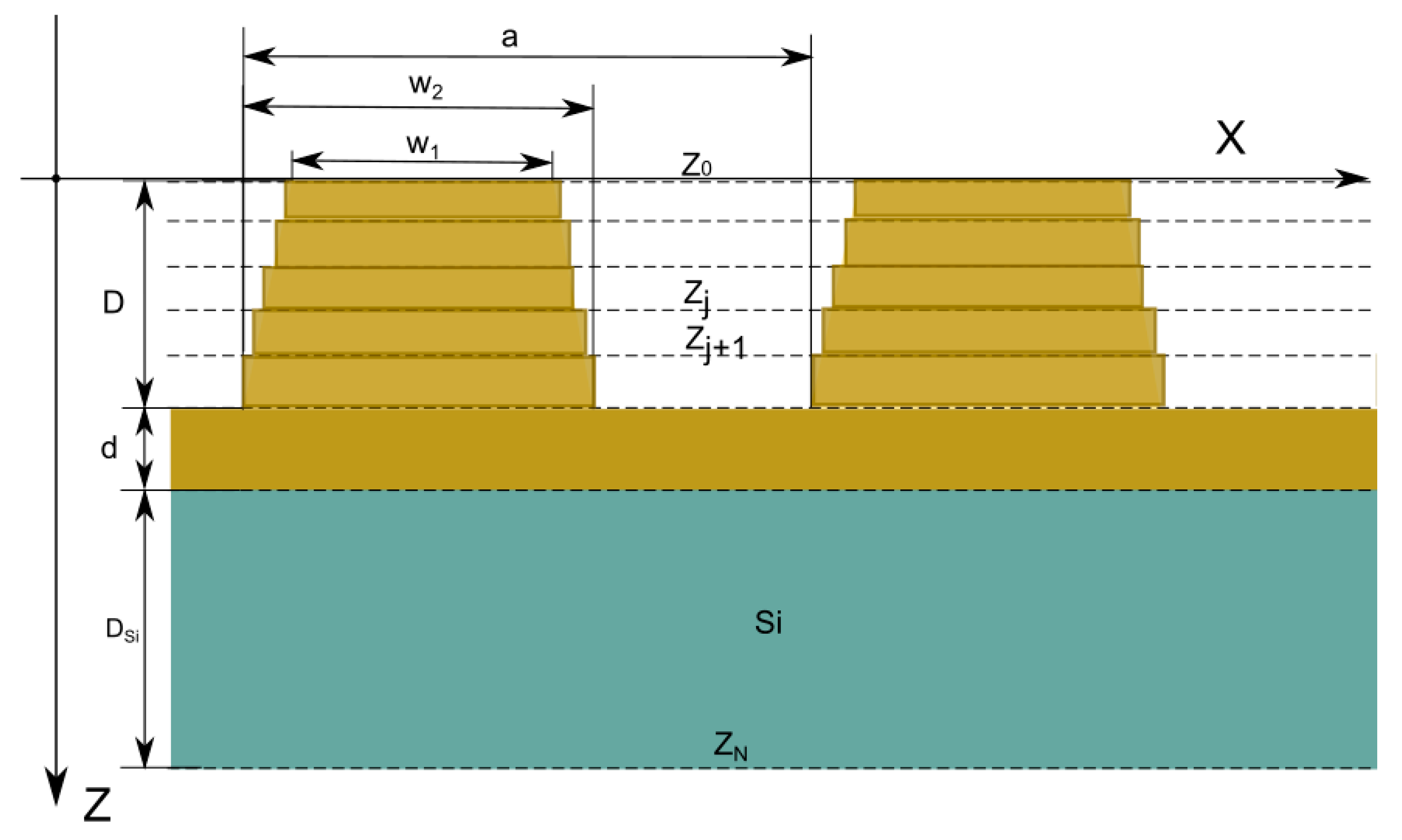
Figure 4.
A schematic sketch of the structure, where a is the grating period, w1 and w2 are the base lengths of the trapezoidal profile, d is the thickness of the intermediate metal layer, and D is the depth of the grating grooves.
3.2. Parameter Estimation from Dispersion Curves
The grating period can be estimated from the phase-matching conditions for SPP excitation for a given angle of incidence and wavelength. If the simulated PPPD is intended for use in an optical smoke detector, then due to the design of this detector, the resonant angle of incidence of the laser beam of the most available laser on the market with a wavelength of 808 nm on the grating (the angle corresponding to the excitation of the SPP) should be equal to θr = 15°. Taking into account the dispersion relations for SPP plasmons, the phase-matching condition for p-polarized laser radiation, the incidence plane of which on the grating is perpendicular to its grooves, can be written as follows:
where is the SPP wavevector, is the surface component of the incident light wavevector, is the dielectric constant of the environment, is the incidence angle, is the grating vector, , and m is an integer (m ≠ 0). Using the approximation of a flat interface between the metal and the dielectric (valid for gratings with shallow relief) for : , where is the dielectric constant of the metal and εd = 1, Expression (1) can be rewritten as follows:
The expression for the grating period is finally obtained as
For the first-order SPP resonance |m| = 1, Expression (3) provides the values a− ≈ 1.1 μm and a+ ≈ 0.63 μm. For the grating with a = 1.1 μm, there is an additional (second) maximum on the angle and spectral dependences of photocurrent, which can be significantly wider than the first one and cause occlusion and blurring of the main maximum. Therefore, it is more convenient to have only one SPP resonance for registering external influences without any interference from the second one. Thus, we chose the grating period a = 0.63 μm.
The sensitivity of the PPPD is primarily affected by the number of photons absorbed in the semiconductor (taking into account the electromagnetic field intensity distribution). To determine this distribution, we carried out a rigorous electrodynamics simulation of the plasmonic structure under consideration.
3.3. Theoretical Method Descriptions
One of the most suitable methods applicable to modeling such periodic structures is RCWA (rigorous coupled-wave analysis) [27], sometimes called FMM (Fourier modal method). We implemented an improved formulation of the RCWA that uses an inverse factorization rule that improves the convergence and speed of calculation for p-polarization [32]. Although this method was developed primarily for simulating rectangular gratings, it can be applicable to a variety of periodic profiles. This can be achieved by reducing an arbitrary periodic profile to a set of thin slices, each of which is approximated by a rectangular profile. This method has advantages compared to methods that use discretization in real space, such as finite element methods or finite difference methods, such as its relative simplicity of implementation and low computational resource requirements. This method allows for the calculation of reflection and transmission coefficients for each diffraction order, as well as the full electric and magnetic near-field distribution.
Since grating is usually deposited on the top of a multilayered structure, it can give rise to numerical instabilities related to the substrate modes. To improve numerical stability, we employed an enhanced transmittance matrix approach [28]. Despite all these improvements, the RCWA method has some drawbacks. For instance, it can converge very poorly and even diverge for metallic gratings with low losses. On the other hand, the presence of a layer with some losses close to the grating can improve convergence because of significant damping.
3.4. Theoretical Framework for Parameter Optimization Problem
Figure 4 illustrates the main geometrical features of the structure and depicts its main parameters, namely the grating period , the groove depth (etching depth) , the intermediated metallic layer depth , and the trapezoidal grating profile bases and . The latter can be expressed through dimensionless parameters, such as the filling factor and the base ratio .
The optimal value for the groove depth was determined from a previous experimental investigation of SPP excitation in aluminum gratings with different modulation patterns [33]. These experiments revealed the optimal ratio of the groove depth to the grating period . Therefore, the optimal groove depth is D ≈ 0.086 × 0.63 μm ≈ 0.05 μm = 50 nm.
The optimal values for the rest of the geometrical parameters were estimated using numerical simulations. In order to better estimate the photoresponse, the amount of electromagnetic energy absorbed in each layer was estimated separately. Such an approach allowed for separating the parasitic absorption in the metal and the useful absorption in the Si substrate.
By knowing the electromagnetic energy distribution inside each layer, we can integrate over the spatial coordinates to find a partial absorption inside the -th layer.
where is the local dielectric constant, is the tangential component of the amplitude of an incident wave, is the local electric field, and are the spatial coordinates.
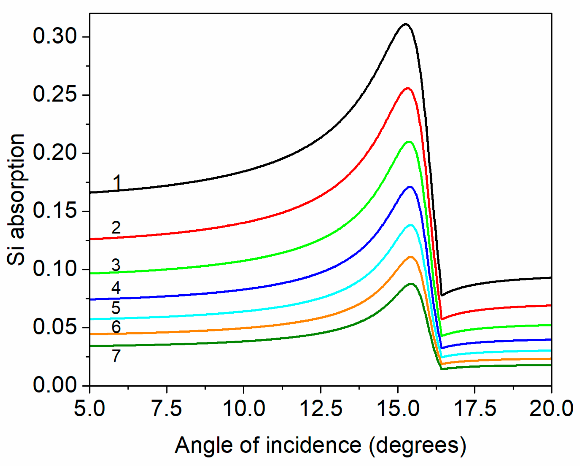
Figure 5 shows the calculated angular dependencies of the “useful” absorption in the Si substrate for the PPPDs with different values of the intermediate layer thickness (d) of the Al grating. A clearly pronounced plasmonic maximum is observed around θres = 15°, corresponding to SPP excitation. The shape of the resonance curve for such structures is closer to a Fano shape, as shown in [20] for gold gratings with a similar groove shape.
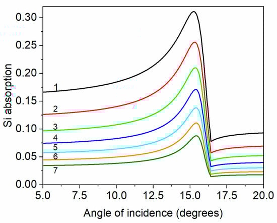
Figure 5.
Angular dependences of light absorption in Si substrate for different values of the intermediate layer thickness for the aluminum-based structures. Other parameters: grating period a = 0.63 μm, etching depth D = 50 nm, and filling factor f = 0.5. Curves 1–7 correspond to thicknesses of 7, 9, 11, 13, 15, 17, and 19 nm, respectively.
Figure 6a (Curve 1) shows the dependence of the maximum light absorption in the silicon substrate (max A(θ)) on d for the simulated structure. A monotonic decrease in the maximum useful absorption was observed with an increase in the thickness of the intermediate Al layer, in agreement with the decrease in its transparency. However, besides maximizing absorption, another parameter had to be optimized to improve the sensitivity, namely the full width at half-maximum (FWHM), because narrower absorption peaks correspond to a steeper change in the detection signal caused by the resonance frequency shift. Figure 6a (Curve 2) shows the dependence of the FWHM on d for the same structure. It is evident that the increase in the thickness of the intermediate Al layer led to a decrease in the FWHM, which is a positive effect. Therefore, it was reasonable to select the goal function taking into account the FWHM; for example, we used the ratio of the maximal absorption to the FWHM, (Figure 6b), in this work.
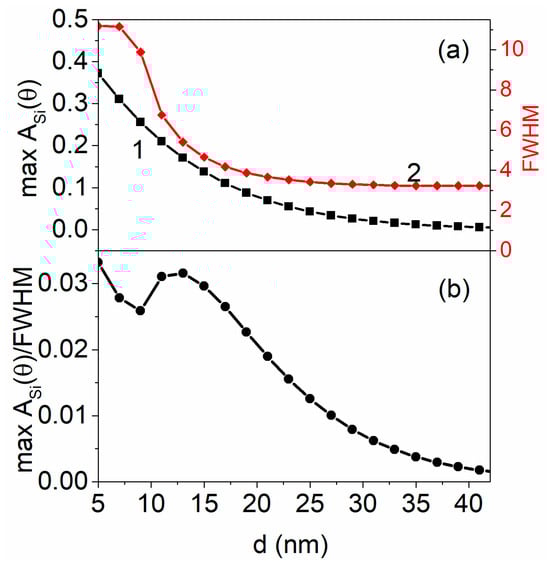
Figure 6.
(a) Dependence of the maximum light absorption in Si (max A(θ)) (Curve 1), and the full width at half-maximum (FWHM) (Curve 2) on the thickness of the intermediate metallic layer d. (b) Dependence of the goal function on d.
The optimal thickness d was found from the analysis of the goal function .
As can be seen in Figure 6b, the goal function has two maxima, namely at a minimum thickness of 5 nm and at around 14 nm. Thermally deposited ultra-thin Al films with an effective thickness of 5 nm practically lose their conductivity after oxidation in the air. At the same time, layers with a thickness of 14 nm are well-passivated and provide efficient excitation of SPPs. Therefore, for the considered structure, d = 14 nm is the optimal thickness of the intermediate Al layer.
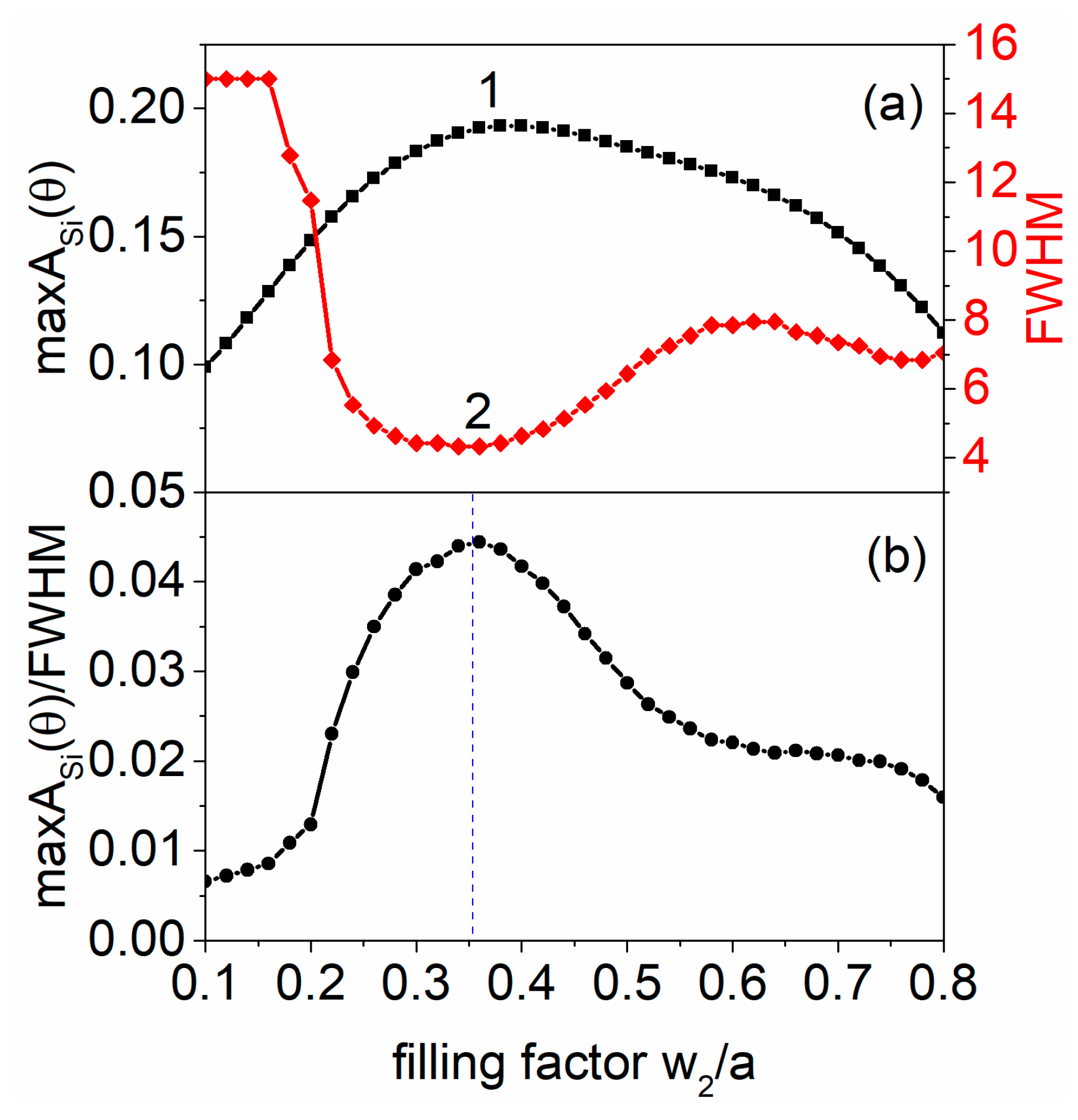
The next parameter of the grating that needs to be optimized is the filling factor . To choose the optimal value of the filling factor, similar calculations of absorption in the Si substrate were carried out for the gratings with different values of . Figure 7a shows the dependencies of the max A(θ) (Curve 1) and FWHM (Curve 2) on the filling factor, which have a non-monotonic character. However, a clear maximum was observed on the dependence of the goal function on the filling factor (Figure 7b), which allowed for determining the optimal value of the filling factor for this structure: = 0.36. Thus, for the considered aluminum grating with an etching depth of 50 nm and a grating period of 0.63 μm, the optimal thickness of the intermediate layer is 14 nm, and the optimal filling factor is 0.36.
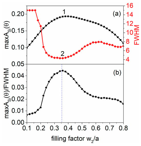
Figure 7.
(a) Dependences of the max A(θ) (Curve 1) and the FWHM (Curve 2) on the grating filling factor. (b) Dependence of the goal function on the grating filling factor. The calculations were carried out at the optimal depth of the intermediate Al layer (14 nm).
4. Results and Discussion
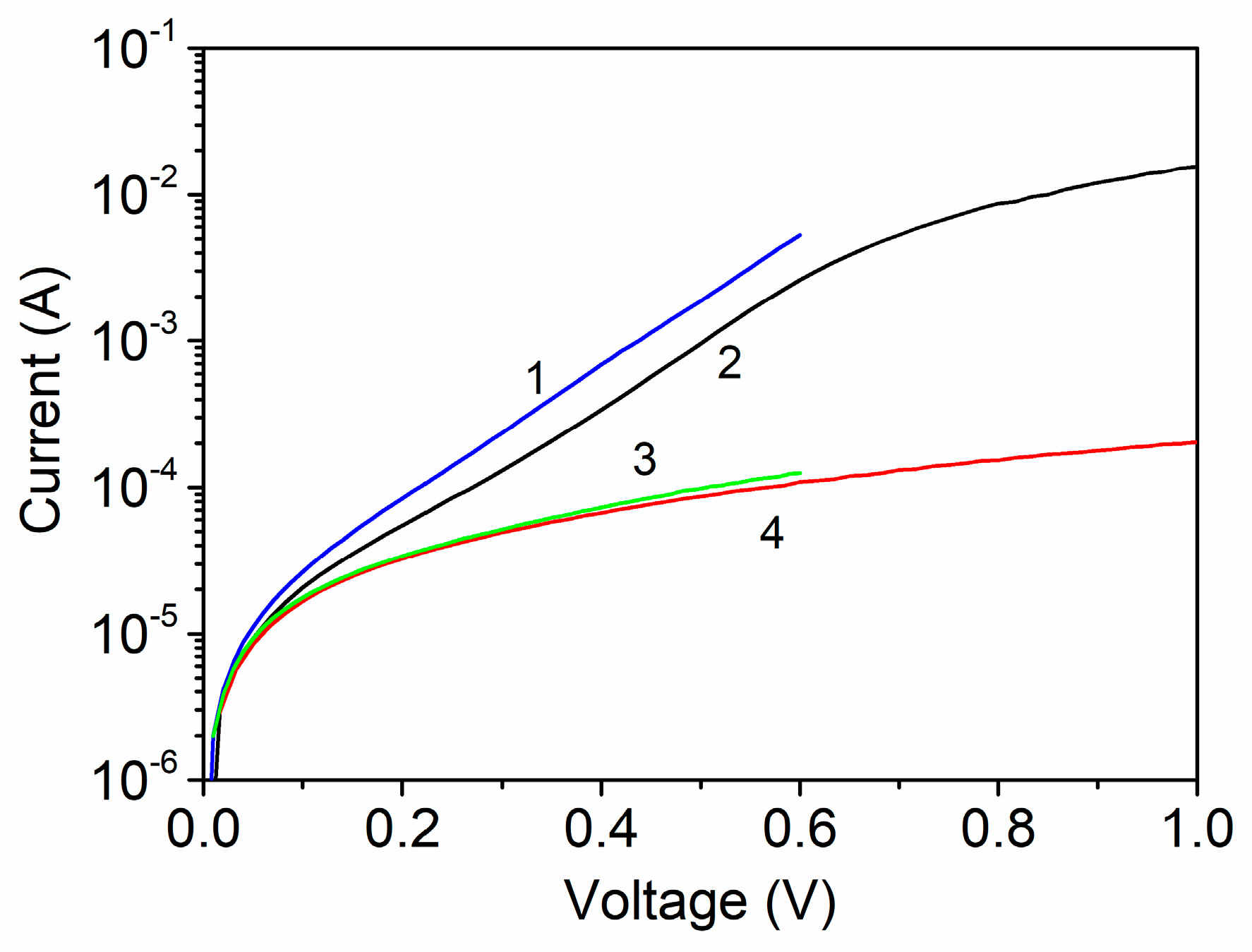
Using the obtained results of theoretical modeling, experimental PPPD samples were fabricated with the above-mentioned optimal parameters of the Al grating. The electrophysical properties of the manufactured PPPDs were investigated by measuring their current–voltage (I–V) characteristics. The I–V characteristics were measured in the dark using a CHI660E (CH Instruments, Bee Cave, TX, USA) workstation in the two-wire connection mode. Figure 8 presents the I–V characteristics of the PPPDs with different frontal contacts (gratings), namely aluminum and gold, for comparison. The rest of the parameters of both PPPDs, including the characteristics of the gratings, were practically the same. It can be seen that the type of metal has little influence on the current–voltage characteristics of the investigated samples.
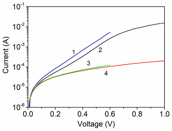
Figure 8.
Forward (1, 2) and reverse (3, 4) current–voltage characteristics of the manufactured PPPD with Au (1, 3) and Al (2, 4) frontal plasmon-active contact.
This indicates that the p-n junction in silicon has a crucial effect on the current. The type of plasmon-active metal on the front surface of the PPPD does not affect the I–V characteristics. Both types of PPPDs, namely with the Au and Al frontal plasmon-active contacts, have almost the same reverse saturation currents and the same slope of the direct I–V characteristics. The differences may be related to the different contact areas and heterogeneity of the properties of the p-n junctions on silicon used for the production of PPPD. Both types of PPPDs have a non-ideality parameter of the I–V characteristics n~4 and a reverse saturation current Io~10−5 A, which describe their diode properties in the range of 0.1–0.6 V by the general law without taking into account the series and shunt resistances:
Here, q is the electron charge, kb is the Boltzmann constant, and T is the temperature.
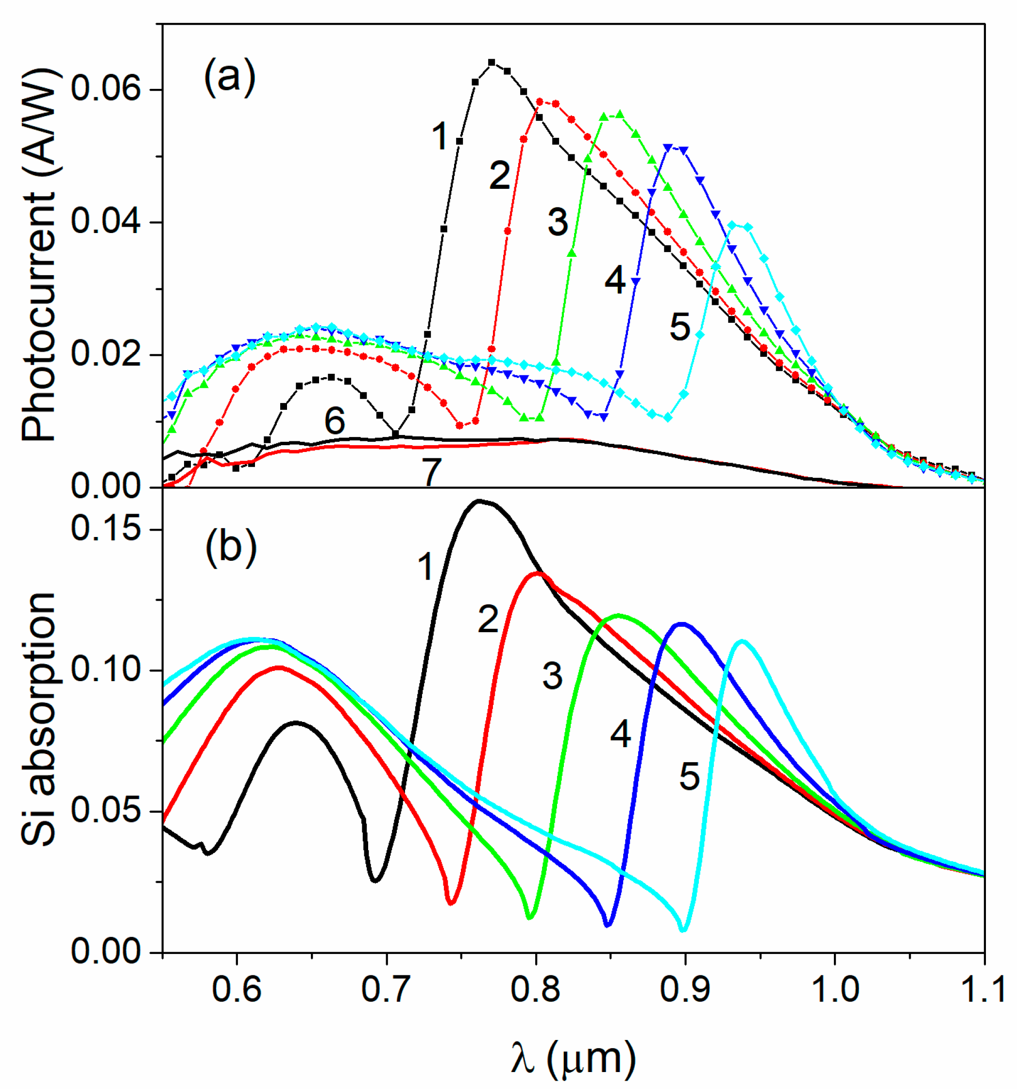
The spectral and angular dependences of the photocurrent for the fabricated PPPDs are presented in Figure 9a,b and Figure 10a,b, respectively. As can be seen in Figure 9a, the PPPD photocurrent exhibits a pronounced resonance for the case of p-polarized light. The resonance peak shifts toward longer wavelengths as the incidence angle increases, as predicted by the respective Expression (2) of the dispersion dependence for a surface plasmon–polariton wave corresponding to an m = +1 diffraction order.
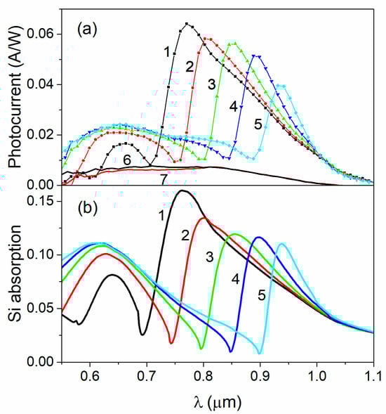
Figure 9.
Spectral (a) dependences of photocurrent for Al-based PPPD in p-polarized light (1–5) and in s-polarized light (6, 7) at different incidence angles: θ = 5° (1, 6), 10° (2), 15° (3), 20° (4), and 25° (5, 7). (b) Numerically simulated Si substrate absorption spectra at the same incidence angles. The photocurrent value is normalized to the power of the incident radiation.
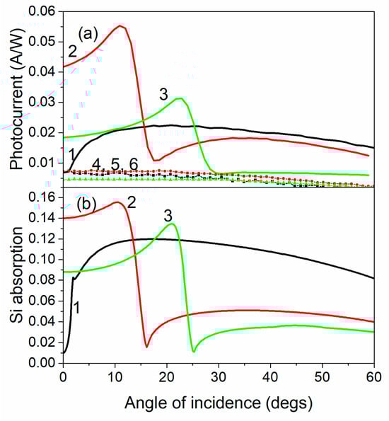
Figure 10.
Angular dependences of photocurrent for Al-based PPPD in p-polarized light (1–3, 1’–3’) and in s-polarized light (4–6) for different wavelengths: 650 nm (1); 808 nm (2); 900 nm (3). (a) Experimentally measured data, and (b) numerically simulated light absorption by Si substrate. The photocurrent value is normalized to the power of the incident radiation.
The polarization sensitivity of the PPPD was determined as the ratio of the photocurrent in resonance in p-polarization to the corresponding value when irradiated with s-polarized light, Ip/Is. For the investigated PPPDs with the optimal parameters of the Al grating, we obtained a value of Ip/Is = 8, an FWHM of the photocurrent spectrum from 50 to 100 nm, and sensitivity at the resonance maximum of Iph = 0.04–0.06 A/W. The obtained PPPD characteristics are comparable to the best characteristics for PPPDs with gold gratings [20]. These practical results open up prospects for replacing gold in the production of PPPD with aluminum, which significantly lowers their cost.
To verify our theoretical model and analyze the underlying physical mechanisms, we compared the experimental results of the photocurrent with the angular and spectral dependences of the light absorption in Si calculated using the RCWA method for a trapezoidal profile (Figure 4) with discretization into N = 10 layers. The calculations were performed for a range of wavelengths and incidence angles corresponding to the experimental conditions.
Our electrodynamic model accounts for all light absorbed within the Si substrate. However, electron–hole pairs generated far from the p-n junction contributed minimally to the photocurrent due to recombination. To address this limitation, we introduced an effective active layer depth, , into the model. This parameter limits the integration range in Equation (4) to . Since it is difficult to derive a heuristic estimate for , we treated it as a free parameter when fitting our model to the experimental data. The optimal value obtained for was 9.2 μm. The above-mentioned optimal parameters of the Al grating were selected as the geometric parameters of the trapezoidal profile.
A direct comparison of the experimental photocurrent spectra (Figure 9a) with the theoretically calculated Si substrate absorption spectra (Figure 9b) reveals a qualitative agreement in the main (1-st order) resonance peak positions and their evolution with the incidence angle. Also, there is a good agreement with respect to the half-width and general shape of the peaks: both the experimental and theoretical first-order resonances have almost identical half-widths. The tendency to the monotonic decrease in the relative peak intensity with the increase in the incidence angle is also reflected in the theoretical calculations. On the other hand, there are some minor discrepancies, namely, in the relative intensity of the second-order (short-wavelength) resonance peaks. These are far more pronounced in the theoretical curves than in the experimental ones. Moreover, the half-width of the second-order resonances is significantly higher. These discrepancies can be related to several factors. First, the conducted electrodynamics simulations provided only the power of absorbed light. Therefore, one should be cautious when comparing these results to the experimentally measured photocurrents. Purely electrodynamics models cannot account for recombination processes; moreover, these processes are spatially dependent because of doping and surface impact, and possible material inhomogeneity. Second, the trapezoidal profile model and the RCWA-layered discretization of the structure profile may also be imperfect approximations. The actual structure profile was much smoother, but such kinds of profiles are much more difficult to model using the RCWA because it requires not only extremely precise profile investigation but also profile discretization with very small steps, which leads to a significant increase in computation time.
A similar comparison of the measured angular photocurrent dependences with the results of the theoretical simulations of absorption in the active Si layer is presented in Figure 10. These curves correspond to three different wavelengths of p-polarized light. Thus, the evolution of the SPP resonance maximum with the frequency/wavelength shift is demonstrated. The structure of the angular absorption dependence is relatively simple: a single asymmetric SPP-related maximum with a dip on the left wing is related to the emergence of the first diffraction order. It is evident in Figure 10 that the Si absorption curves repeat the shape of the experimental photocurrent dependences with some small deviations, probably due to the profile approximation as mentioned above.
The close agreement between the experimental and theoretical results demonstrates validity of the RCWA method in describing the optical response of PPPDs. However, there may be some discrepancies in the peak intensities and half-widths, which may have been caused by factors such as manufacturing imperfections, material heterogeneity, or theoretical model limitations, such as the use of an approximate trapezoidal profile and neglecting the charge carrier recombination processes on surfaces and defects.
5. Conclusions
Using the RCWA method, theoretical simulations of the electromagnetic field intensity distribution in a PPPD based on silicon p-n junctions and periodically textured aluminum as the plasmon-carrying metal were performed. This made it possible to optimize the parameters of the plasmon-carrying grating layer in order to increase the sensitivity of the PPPD. Experimental samples of the PPPD with aluminum gratings were manufactured, and their characteristics were studied. For the PPPDs with optimal grating parameters, a polarization sensitivity value of Ip/Is = 8, an FWHM of the resonance in the photocurrent spectrum ranging from 50 to 100 nm, a sensitivity at the resonance maximum of Iph = 0.04–0.06 A/W, and an angular half-width of the photocurrent resonance of Δθ = 5° were obtained. These characteristics are comparable to the best characteristics achieved with PPPDs using gold gratings. The obtained results pave the way for replacing gold with aluminum in PPPD production, significantly reducing their cost.
Author Contributions
Conceptualization and data curation, S.M., I.I. and Y.L.; methodology, I.I. and S.M.; software, Y.L.; formal analysis and investigation, V.M., V.R., I.M., R.R., M.D., Y.S., V.T., O.S. and D.K.; writing—original draft preparation and writing—review and editing, S.M., I.I. and Y.L.; project administration and funding acquisition, S.M. All authors have read and agreed to the published version of the manuscript.
Funding
This work was partially supported by the National Research Foundation of Ukraine (Grant No. 2022.01/0126, “Development and implementation of a dust-insensitive smoke detector based on a plasmon-polariton photodetector”). S.M. appreciates funding from the Ministry of Education and Science of Ukraine (Project No. 0122U001956).
Institutional Review Board Statement
Not applicable.
Informed Consent Statement
Not applicable.
Data Availability Statement
The raw data supporting the conclusions of this article will be made available by the authors on request.
Acknowledgments
The authors are grateful to P. Lytvyn and A. Korchovyi for the AFM analysis, and O. Kondratenko for the spectroscopic ellipsometry measurements.
Conflicts of Interest
The authors declare no conflicts of interest.
References
- Gramotnev, D.K.; Bozhevolnyi, S.I. Plasmonics beyond the diffraction limit. Nat. Photonics 2010, 4, 83–91. [Google Scholar] [CrossRef]
- Homola, J. Surface plasmon resonance sensors for detection of chemical and biological species. Chem. Rev. 2008, 108, 462–493. [Google Scholar] [CrossRef] [PubMed]
- Sipe, J.; Becher, J. Surface-plasmon-assisted photoemission. JOSA 1981, 71, 1286–1288. [Google Scholar] [CrossRef]
- Tamm, I.; Dawson, P.; Sellai, A.; Pate, M.; Grey, R.; Hill, G. Analysis of surface plasmon polariton enhancement in photodetection by Al—GaAs Schottky diodes. Solid-State Electron. 1993, 36, 1417–1427. [Google Scholar] [CrossRef]
- Guo, J.; Wu, Z.; Li, Y.; Zhao, Y. Design of plasmonic photodetector with high absorptance and nano-scale active regions. Opt. Express 2016, 24, 18229–18243. [Google Scholar] [CrossRef] [PubMed]
- Wu, M.; Xu, N.; Wang, E.; Gen, S.; Zhu, H.; Liu, C.; Cao, J. Nanogratings fabricated by wet etching assisted femtosecond laser modification of silicon for surface plasmon resonance sensing. Appl. Surf. Sci. 2022, 603, 154446. [Google Scholar] [CrossRef]
- Alavirad, M.; Roy, L.; Berini, P. Surface plasmon enhanced photodetectors based on internal photoemission. J. Photonics Energy 2016, 6, 042511. [Google Scholar] [CrossRef]
- Brueck, S.; Diadiuk, V.; Jones, T.; Lenth, W. Enhanced quantum efficiency internal photoemission detectors by grating coupling to surface plasma waves. Appl. Phys. Lett. 1985, 46, 915–917. [Google Scholar] [CrossRef]
- Gosciniak, J.; Atar, F.B.; Corbett, B.; Rasras, M. Plasmonic Schottky photodetector with metal stripe embedded into semiconductor and with a CMOS-compatible titanium nitride. Sci. Rep. 2019, 9, 6048. [Google Scholar] [CrossRef]
- Sharma, A.K.; Pandey, A.K. Au grating on SiC substrate: Simulation of high performance plasmonic Schottky barrier photodetector in visible and NIR regions. J. Phys. D Appl. Phys. 2020, 53, 175103. [Google Scholar] [CrossRef]
- Saito, Y.; Yamamoto, Y.; Kan, T.; Tsukagoshi, T.; Noda, K.; Shimoyama, I. Electrical detection SPR sensor with grating coupled backside illumination. Opt. Express 2019, 27, 17763–17770. [Google Scholar] [CrossRef] [PubMed]
- Glass, A.; Liao, P.; Johnson, A.; Humphrey, L.; Lemons, R.; Olson, D.; Stern, M. Periodically structured amorphous silicon detectors with improved picosecond responsivity. Appl. Phys. Lett. 1984, 44, 77–79. [Google Scholar] [CrossRef]
- Berthold, K.; Beinstingl, W.; Berger, R.; Gornik, E. Surface plasmon enhanced quantum efficiency of metal-insulator-semiconductor junctions in the visible. Appl. Phys. Lett. 1986, 48, 526–528. [Google Scholar] [CrossRef]
- Brongersma, M.L. Plasmonic photodetectors, photovoltaics, and hot-electron devices. Proc. IEEE 2016, 104, 2349–2361. [Google Scholar] [CrossRef]
- Berini, P. Surface plasmon photodetectors and their applications. Laser Photonics Rev. 2014, 8, 197–220. [Google Scholar] [CrossRef]
- Huang, J.A.; Luo, L.B. Low-dimensional plasmonic photodetectors: Recent progress and future opportunities. Adv. Opt. Mater. 2018, 6, 1701282. [Google Scholar] [CrossRef]
- Jestl, M.; Köck, A.; Beinstingl, W.; Gornik, E. Polarization-and wavelength-selective photodetectors. JOSA A 1988, 5, 1581–1584. [Google Scholar] [CrossRef]
- Dmitruk, N.; Mayeva, O.; Mamykin, S.; Yastrubchak, O.; Klopfleisch, M. Characterization and application of multilayer diffraction gratings as optochemical sensors. Sens. Actuators A Phys. 2001, 88, 52–57. [Google Scholar] [CrossRef]
- Dmitruk, N.; Borkovskaya, O.Y.; Mayeva, O.; Fursenko, O. Polarization-sensitive photocurrents of metal-semiconductor structures with flat and microrelief interfaces. Microelectron. J. 1996, 27, 37–42. [Google Scholar] [CrossRef]
- Korovin, A.V.; Dmitruk, N.L.; Mamykin, S.V.; Myn’ko, V.I.; Sosnova, M.V. Enhanced dielectric environment sensitivity of surface plasmon-polariton in the surface-barrier heterostructures based on corrugated thin metal films with quasi-anticorrelated interfaces. Nanoscale Res. Lett. 2017, 12, 217. [Google Scholar] [CrossRef]
- Gnilitskyi, I.; Mamykin, S.; Dusheyko, M.; Borodinova, T.; Maksimchuk, N.; Orazi, L. Diffraction Gratings Prepared by HR-LIPSS for New Surface Plasmon-Polariton Photodetectors & Sensors. In Proceedings of the Frontiers in Optics, Rochester, NY, USA, 17–21 October 2016; p. JW4A.88. [Google Scholar]
- Dmitruk, N.; Klopfleisch, M.; Mayeva, O.; Mamykin, S.; Venger, E.; Yastrubchak, O. Multilayer diffraction gratings Al/GaAs as polaritonic photodetectors. Phys. Status Solidi A 2001, 184, 165–174. [Google Scholar] [CrossRef]
- Gérard, D.; Gray, S.K. Aluminium plasmonics. J. Phys. D Appl. Phys. 2014, 48, 184001. [Google Scholar] [CrossRef]
- Knight, M.W.; King, N.S.; Liu, L.; Everitt, H.O.; Nordlander, P.; Halas, N.J. Aluminum for plasmonics. ACS Nano 2014, 8, 834–840. [Google Scholar] [CrossRef] [PubMed]
- Ibrahim, J.; Al Masri, M.; Veillas, C.; Celle, F.; Cioulachtjian, S.; Verrier, I.; Lefèvre, F.; Parriaux, O.; Jourlin, Y. Condensation phenomenon detection through surface plasmon resonance. Opt. Express 2017, 25, 24189–24198. [Google Scholar] [CrossRef]
- Gao, Y.; Murai, S.; Shinozaki, K.; Ishii, S.; Tanaka, K. Aluminum for near infrared plasmonics: Amplified up-conversion photoluminescence from core–shell nanoparticles on periodic lattices. Adv. Opt. Mater. 2021, 9, 2001040. [Google Scholar] [CrossRef]
- Moharam, M.; Gaylord, T.K. Rigorous coupled-wave analysis of planar-grating diffraction. JOSA 1981, 71, 811–818. [Google Scholar] [CrossRef]
- Moharam, M.; Pommet, D.A.; Grann, E.B.; Gaylord, T.K. Stable implementation of the rigorous coupled-wave analysis for surface-relief gratings: Enhanced transmittance matrix approach. JOSA A 1995, 12, 1077–1086. [Google Scholar] [CrossRef]
- Watts, R.; Sambles, J.; Hutley, M.; Preist, T.; Lawrence, C. A new optical technique for characterizing reference artefacts for surface profilometry. Nanotechnology 1997, 8, 35. [Google Scholar] [CrossRef]
- Palik, E.D. Handbook of Optical Constants of Solids; Academic Press: Cambridge, MA, USA, 1998; Volume 3. [Google Scholar]
- Dan’ko, V.; Dmitruk, M.; Indutnyi, I.; Mamykin, S.; Myn’ko, V.; Shepeliavyi, P.; Lukaniuk, M.; Lytvyn, P. Au gratings fabricated by interference lithography for experimental study of localized and propagating surface plasmons. Nanoscale Res. Lett. 2017, 12, 190. [Google Scholar] [CrossRef]
- Lalanne, P.; Morris, G.M. Highly improved convergence of the coupled-wave method for TM polarization. JOSA A 1996, 13, 779–784. [Google Scholar] [CrossRef]
- Indutnyi, I.Z.; Mynko, V.I.; Sopinskyy, M.V.; Dan’ko, V.A.; Lytvyn, P.M. Investigation of the surface plasmon-polaritons excitation efficiency on aluminum gratings taking into account diffracted radiation. Optoelectron. Semicond. Tech. 2021, 1, 71–82. [Google Scholar]


Disclaimer/Publisher’s Note: The statements, opinions and data contained in all publications are solely those of the individual author(s) and contributor(s) and not of MDPI and/or the editor(s). MDPI and/or the editor(s) disclaim responsibility for any injury to people or property resulting from any ideas, methods, instructions or products referred to in the content. |
© 2024 by the authors. Licensee MDPI, Basel, Switzerland. This article is an open access article distributed under the terms and conditions of the Creative Commons Attribution (CC BY) license (https://creativecommons.org/licenses/by/4.0/).