Abstract
This paper presents a comprehensive review of the design and implementation methods of low-power piezoelectric energy harvesting circuits, which in the last few years have gained an extremely large range of applications like the power sources of wearable electronic devices, such as biometrical sensors. Before examining the electronic circuitries of the self-supplied power devices, an overview of the structure, equivalent electrical circuits, and basic parameters of the piezoelectric generators and MEMSs as energy harvesting elements is presented. The structure of energy storage elements (parallel-plate capacitors and thin-film supercapacitors), suitable for this type of application, is also presented. The description of these components from an electrical point of view allows them to be easily workable when connected to the various power conversion electronic circuits. Based on an overview of the structure and the principles of operation, as well as some analytical expressions for energy efficiency evaluation, a comprehensive comparative analysis is presented. Depending on the advantages and disadvantages of the known circuit configurations, the basic electrical and design parameters are systematized in tabular form. Practical realizations of piezoelectric power conversion circuits are also presented in graphic form, ensuring the optimal value of energy efficiency and compactness in the construction of the devices.
1. Introduction
In the last few years, a large number of wearable electronic devices have appeared in the specialized scientific literature. Moreover, these devices have various practical applications. For example, most of them are for medical purposes [1,2,3], to determine various biometric parameters, as well as to study the behavior of the human body. There are also wearable electronic devices designed to determine, for example, the location, speed, and acceleration of various vehicles [4,5,6,7,8] or monitor electrical and non-electrical parameters in an industrial environment by wireless sensor nodes (WSNs) [9,10,11]. All the wearable devices listed above require a certain power supply device (PSD) with the following general technical specifications: First, the power supply sources have to provide a constant value of the DC output voltage and current under variations in the ambient temperature and the levels of the input signals, produced by piezoelectric, electromagnetic, electrostatic, or triboelectric elements. Second, the power supply devices have to work with a high coefficient of efficiency (for example, higher than 50%) or with relatively low power dissipation (for example <0.01 W). Third, the power sources have to include functional blocks for short circuits or thermal overload protection of the output transistors. Also, the sources have to provide charging of a low-power rechargeable battery or supercapacitor, and the use of an additional battery (or backup primary battery) has to be implemented only in cases where the energy of the input source is insufficient.
The review of recent achievements in the field of the design of wearable electronic devices shows a wide variety of technical solutions for the implementation of stand-alone power sources with the specific electronic circuitries of Power Path Management Systems or Circuits (PMSs or PMCs). Some of these use commercially available application-specific integrated circuits that include functions for both AC-to-DC voltage conversion and DC/DC regulation providing a charge signal to low-power rechargeable batteries or supercapacitors. Others use custom-designed power supplies that are a functional block of a specialized electronic module implemented as a monolithic integrated circuit. For both power source implementations, additional recommendations are needed to select appropriate circuit configurations and sizing formulas depending on the parameters of the input signal source and the load in the output. For both variants of the implementation of power sources, additional recommendations are needed for the selection of appropriate circuit configurations and formulas for the selection of component values of a certain circuit depending on the parameters of the input signal source and the output load.
In order to satisfy the above-mentioned need, an analysis of published review papers [12,13,14,15,16,17,18,19,20,21,22] has been performed. Moreover, the published review articles can be divided into two groups in view of the trends related to the continuous improvement in the approaches to designing electronic circuits, as well as the synthesis of new materials for the construction of piezoelectric elements. The first group of publications [12,13,14,15,16] reported in international scientific journals covers the period of the last ten years. In these publications, the focus of the authors’ attention is mainly on the structure and principle of operation of piezoelectric elements. Also, the methods and technologies for building piezoelectric elements are examined in great depth, discussing various types of materials and the criteria for choosing the optimal option depending on specific applications. When considering the electronic circuits specially designed for piezoelectric energy harvesters, in most cases, the input stages implemented on the basis of voltage rectifiers with a series-connected inductor and electronic switch to increase the voltage amplitude are considered. This type of specific input stage, which is used to convert AC voltage into DC voltage, is required relatively often since the energy that is obtained from piezoelectric elements depends on the presence of spontaneously occurring mechanical vibrations. The second group of publications [17,18,19,20,21,22] includes review articles reported in international scientific journals during the last year. In these publications, the attention of the authors is basically directed to consider approaches and techniques for the design and use of wearable electronic devices, as well as the capabilities of wireless connection with data acquisition systems. In a brief form, the structure and principles of the operation of circuit configurations suitable for building power management systems are considered. Furthermore, some of the publications [17,20,21] analyze and compare in tabular form the basic structural or electrical parameters of various types of piezoelectric elements or power management systems, confirming their effectiveness.
The lack of detailed analysis of the electronic circuits intended for the electrical energy harvesters is largely due to the very specific requirements for circuit configurations since the input signal is pulsed in nature, i.e., in the general case, the voltage is with a non-sinusoidal waveform. When the supply voltage has a pulsed (discontinuous) form, the relationships between voltages and currents in the circuits significantly change quantitatively and, in some cases, qualitatively. Also, the values of voltages and currents are often relatively small, so, for example, the DC voltage after the rectifier has values up to 10 V, and the current values are in most cases less than 1 mA [7,8,9,10,11]. As a result, it is relatively difficult to cover in a theoretical way the issue related to the selection of a specific circuit configuration and selecting component values for a certain configuration.
In this paper, based on known theoretical methods, as well as various circuit configurations, the authors attempt to present a detailed analysis of different circuit solutions suitable for the implementation of low-power sources used as alternative stand-alone sources of electrical energy. Furthermore, the focus of the authors’ attention is directed to energy sources in which mechanical vibrations are converted into input AC voltage using piezoelectric generators. Taking into account the specifics of the input sources, in the process of considering the various circuit solutions, emphasis is placed on the circuit design process according to given requirements and their practical applications.
This paper is organized as follows: The next section examines the structure, principle of operation, and basic equivalent electrical circuits of low-power piezoelectric elements. A brief description of commonly used commercially available thick-film piezoelectric generators is also given. Section 3 presents detailed information on the various types of micro-power electronic converters; the first subsection analyzes the most commonly used voltage rectifiers and multipliers (doublers and quadruplers). In the next subsection, the basic approaches to building low-power switching DC-DC regulators are presented. In the third subsection, two variants for implementing block diagrams of PWM controllers are also given. The circuit configurations of the step-down and step-up converters are analyzed in detail. In the last subsection, the structure, principle of operation, and practical implementation of the most commonly used industrial monolithic micro-power electronic converters are analyzed. Section 4 presents the structure of parallel-plate capacitors as well as their equivalent circuits with their basic analytical expressions. In the same section, based on parallel-plate capacitors, a description of electrochemical double-layer capacitors with an equivalent circuit diagram suitable for the design process is given. Section 5 is dedicated to a comparative analysis of previously published electronic circuits of power management systems in which different types of piezoelectric elements are used as input signal sources. Comparative characteristics and parameters are presented in tabular form. Section 6 presents commercially available monolithic integrated circuits and more important electronic circuits developed by scientific teams, given in graphic form, with comments on their advantages and disadvantages. The concluding remarks of this paper as well as directions for future work are given in Section 7.
2. Piezoelectric Harvesters (PEHs)
2.1. Piezoelectric Generators—Equivalent Circuits and Basic Parameters
Piezoelectric generators are electro-mechanical elements for which the energy of mechanical vibrations is converted into electrical energy. The piezoelectric materials consist of asymmetrical unit cells within their crystal lattice structures. These asymmetrical unit cells include atoms or molecules with a center of positive and negative charges within the cell that do not coincide, thus creating a permanent dipole moment. This internal arrangement allows piezoelectric materials to respond to external mechanical and electrical stimuli by generating electric polarization [2,23].
In order to use the piezoelectric elements, the most widely spread structure, due to its compatibility with the silicon microfabrication technology, is the cantilever. This is a flexible beam coated with piezoelectric material so that mechanical vibrations are produced when driven, and an electrical AC voltage is generated between both sides of the element (Figure 1), to which electrodes are mounted [24,25,26,27]. Depending on the structure of the harvesters, this electrical voltage is proportional basically to the amplitude and frequency of the mechanical vibrations (Figure 2). When an external force is applied, resulting in vibrations of sinusoidal waveform and constant amplitude (maximum deflection of the beam) , the static charge equation is [25]
where u is the tip deflection of the cantilever, is the voltage, generated between the two electrodes of the piezoelectric element, is the coupling coefficient of the beam geometry, and is the internal electrode capacitance of the PEH.

Figure 1.
Simplified diagram of a piezoelectric element fixed to a flexible beam (cantilever).

Figure 2.
Piezoelectric element connected to a load.
If the terminals of the electrodes of the piezoelectric element are connected to a load with certain parameters in the network flow, there is a current whose value is given by the following formula:
As can be seen from Formula (2), the piezoelectric element can be represented as a current generator and a capacitor . Moreover, for sinusoidal excitation of the cantilever, the current is also sinusoidal in shape , and the amplitude has the form . Then, the amplitude of the current is proportional to the geometry of the cantilever expressed by the value of the coefficient , and it is also proportional to the amplitude and frequency ω of the mechanical vibrations.
The electrical energy that can be obtained at the maximum (peak) value of the voltage can be given as
Then, based on the above value, the maximum average power (or raw power) that can be obtained from a piezoelectric element is
Based on the structures given in Figure 1 and Figure 2, Figure 3 shows the equivalent circuit diagram of a piezoelectric element. Figure 3a shows an equivalent circuit according to Norton’s theorem, showing a current source and a capacitor connected in parallel with it, and Figure 3b shows an equivalent circuit according to Thévenin’s theorem, in which a current source is converted into a voltage source and a capacitor is connected in series with it. For the equivalent circuit in Figure 3b, the voltage of the piezoelectric element is found, .
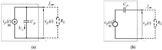
Figure 3.
Equivalent circuit diagram of a piezoelectric element: (a) circuit variant using a current source, according to the Norton theorem; (b) circuit variant using voltage source, according to Thévenin’s theorem.
Impedance matching is a necessity in systems where the load is required to use the maximum power generated by the source. In energy harvesting systems, however, the generated energy is not fully used to power the load at the time of its generation, and it must also be stored. In [28], the authors describe in depth the steps for analyzing the matching of the piezoelectric source to the load in these systems. They begin by analyzing the mechanical system and deriving the equivalent electrical circuit, then analyze the load circuit with several energy conversion options with an analytical and graphical representation in the complex plane of each. In the complete electrical equivalent circuit of the piezoelectric load system shown in Figure 4, veq(t), XL, XC, and R are the source equivalent model parameters, corresponding to the mechanical parameters of velocity, mass, damping, and stiffness, and XE, Rd, and Rh are the electrical part parameters.
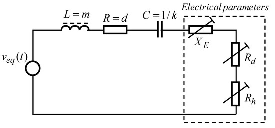
Figure 4.
Simplified circuit configuration of system piezoelectric energy harvester.
In it, it is noticed that the values are not only variable but also dependent on each other. Rd and Rh have the same electrical function of an active load but differ in that losses are denoted by Rd and harvested energy by Rh. They propose a Formula (5) that describes the dependence of the harvested energy Ph on the parameters in the equivalent circuit, where Veq is the magnitude of the equivalent source Veq, and Zsys is the impedance seen by it.
where in the mechanical domain veq is the equivalent voltage source, XL = ωL (the equivalent inductor L = m takes into account the effective beam mass m [kg] or the inertia of the generator), the equivalent resistance R = d (d [kg/s]) represents the mechanical damping, XL = 1/ωC (the equivalent capacitor C = 1/k represents the reciprocal mechanical stiffness k [N/m]), and XE is the reactance of the electrical part of the PEH (the values of Rd, Rh, and XE are not only variables (denoted with arrows) but also related with each other (illustrated with dot links among the three components)).
As a consequence of this formula, they present the condition for achieving maximum power in the general case, presented as the Formula (6).
2.2. Commercially Available Piezoelectric Elements
Examples of commercially available piezoelectric elements that can be used to build low-power alternative sources of electrical energy are ABT-441-RC [29] and ABT-448-90-RC [30]. For them, the outer diameter is no larger than 35 mm, and the generated sinusoidal voltage on the electrodes in a resonance has maximum value for the amplitude. The equivalent internal electrode capacitance is approximately 20 nF ± 30%. The natural resonant frequency is up to 3 kHz, and the equivalent resonant resistance is higher than 200 Ω. The operating temperature range of the piezoelectric elements is from −20 °C to +70 °C, and the parameters listed above are determined at a temperature of 25 °C. Based on laboratory experimental studies performed with ABT-441-RC at frequencies lower than the resonance frequency, the amplitude of the produced non-sinusoidal voltage (in the presence of higher harmonics) can have lower values, and the internal resistance reaches values of up to tens of kiloohms. Thus, the piezoelectric element can be considered more like a current source with internal resistance and capacitance, according to the equivalent circuit in Figure 3a. For ABT-448-90-RC, a third terminal has been added that can be used in a feedback circuit. In the generator mode of operation, this terminal can be left unconnected. To design electronic converters, it is essential to use equivalent electrical circuits in which the behavior of real devices is modeled with sufficient accuracy.
Another frequently used group of low-power piezoelectric elements that convert mechanical vibrations or shocks into AC voltage are the PPA (Piezo Protection Advantage) generators of the Mide Technologies® company [31]. The PPA elements from Mide Technologies® (Woburn, MA, USA) are mounted in rectangular packages and are designed for cantilevers or fixed-beam configurations. Each of the products has a wide range of resonant frequencies from as low as 20 Hz up to 500 Hz. All elements will operate at virtually any frequency in actuation. In energy harvesting, they will need at least 2 Hz of motion to produce any electrical current. They are virtually unlimited in regard to higher frequencies. Moreover, they can generate a few mA of current at several volts of output voltage.
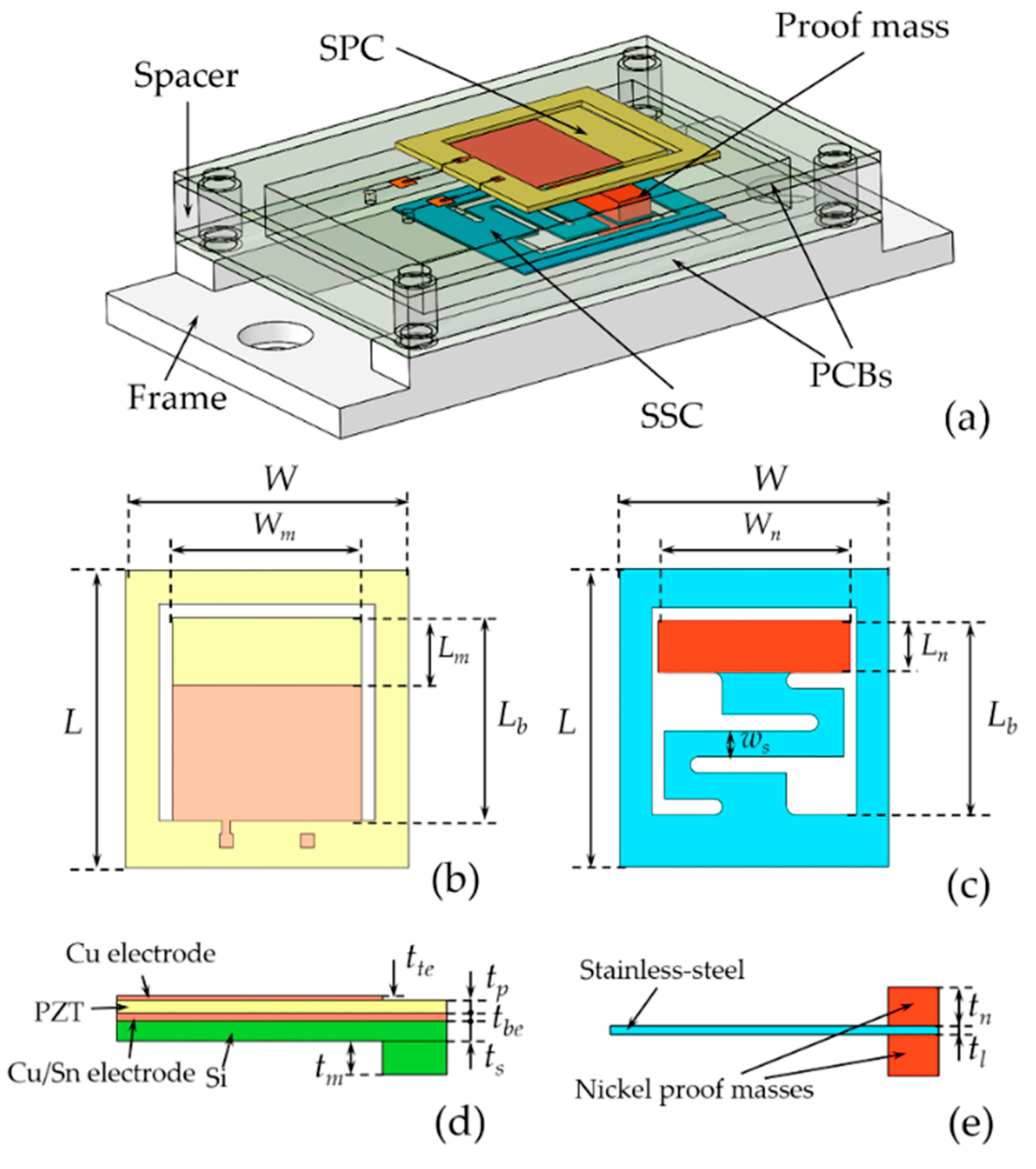
2.3. Micro-Electro-Mechanical System (MEMS) Piezoelectric Energy Harvesting Elements
The MEMSs have revolutionized the field of energy harvesting, providing highly efficient and compact solutions for powering small electronic devices [32,33]. When compared to traditional flexible-foil-based wearable piezoelectric generators, MEMS piezoelectric energy harvesting elements offer several distinct advantages. Specifically, silicon-based MEMS piezoelectric energy harvesting devices excel in their miniaturization and precise control over dimensions, allowing for enhanced energy conversion efficiencies and sensitivity to mechanical stimuli. These devices can be tailored to resonate at specific frequencies, optimizing energy extraction from various mechanical inputs, such as vibrations. This level of customization sets MEMS piezoelectric harvesters apart from their flexible foil counterparts, enabling them to operate in a wider range of conditions and environments (Figure 5).
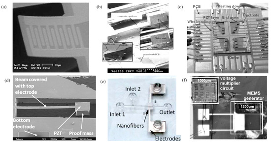
Figure 5.
Different MEMS piezoelectric energy harvesting devices including (a) thin-film PZT cantilever, (b) high-aspect-ratio microbeam, (c) cantilever array, (d) silicon oxide wafer-based cantilever, (e) microfluidic harvester, and (f) harvester with rectangular hole [34].
The versatility of MEMS piezoelectric energy harvesters extends to their ability to generate electrical power from diverse mechanical sources, including ambient vibrations, structural deformations, and even human motion. This broad spectrum of energy sources makes MEMS devices well suited for applications where continuous but low-magnitude vibrations are present, offering a reliable power source for a variety of portable electronics and sensors. While specific ranges for each parameter of silicon piezoelectric MEMS harvesters can vary based on the design, application, and fabrication process, here are typical ranges for some key performance parameters [35,36]:
- -
- Energy conversion efficiency: This is a key factor in determining the overall performance of the harvester in converting mechanical vibrations into electrical energy, which is very often expressed by the output power or by power density for an activated volume of material. In this regard, typical values for the output power are in the range of 800 nW to 14 W [32], according to the cantilever shape and the material’s crystal structure and thickness, and for the power density, they are in the range of 3 μW/mm3–3 mW/cm3 [37].
- -
- Size/dimensions: These devices can be miniaturized to dimensions ranging from a few millimeters down to sub-millimeter scales, with thicknesses typically falling in the range of tens to hundreds of micrometers. These compact sizes enable integration into small-scale systems and applications where space is limited, offering versatility and flexibility in deployment. With the silicon MEMS harvesters, it is possible to maintain high aspect ratios, where the thickness of the device is significantly smaller than its lateral dimensions. This characteristic enables the harvester to effectively convert mechanical vibrations into electrical energy while maintaining structural integrity and mechanical robustness. The high-aspect-ratio design also enhances the harvester’s sensitivity to vibrations, optimizing its energy harvesting performance across a wide range of frequencies.
- -
- Frequency range: Silicon MEMS harvesters can be tuned to resonate at frequencies ranging from a few hertz (Hz) to several kilohertz (kHz), allowing for efficient energy extraction from a broad spectrum of mechanical vibrations, such as for structural health monitoring, wearable technologies, transportation systems, and industrial machinery. By adjusting the dimensions, material properties, and structural configurations of the harvester, engineers can tailor its resonant frequency to match the dominant frequencies present in the ambient vibration source.
- -
- Reliability: Silicon-based MEMS devices are known for their high reliability, with the mean time between failures (MTBF) exceeding tens of thousands of operational hours. This reliability ensures stable performance over an extended operational lifespan. The materials used in their construction, such as silicon substrates and piezoelectric thin films, exhibit excellent mechanical properties and resistance to environmental factors like temperature fluctuations, humidity, and vibration stresses. This inherent durability enables silicon MEMS harvesters to maintain their energy conversion efficiency and functionality over an extended operational lifespan, making them ideal for applications requiring continuous and reliable energy harvesting capabilities, such as in industrial, automotive, aerospace, and environmental monitoring environments.
- -
- Scalability: Silicon MEMSs’ fabrication processes enable the production of harvesters in large quantities, ranging from individual devices for specialized applications to arrays of harvesters for increased power output. Scalability allows for cost-effective manufacturing and deployment in various scenarios, which is demonstrated in Figure 6, where scalability refers to the ability of a MEMS energy harvester to be produced and deployed with a minimal quantity of materials and energy (low resource input) while also maintaining its efficiency even for critical parameters, such as low frequencies with no need for using a macrobeam. By being scalable, the technology can be easily adapted and manufactured in varying quantities and sizes (micro or nano) without significantly increasing costs. This means that as the production volume or deployment scenarios change, the cost per unit or efficiency does not increase proportionally, making it an attractive and economically viable solution for mass production and deployment in various scenarios, which is visible in Figure 7, because it is a small version of millimetric beam design.
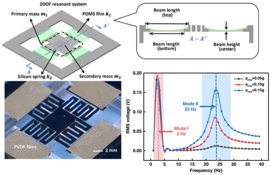
Figure 6.
Complex MEMS piezoelectric energy harvester, which reaches ultralow-frequency resonance [38].
Figure 6.
Complex MEMS piezoelectric energy harvester, which reaches ultralow-frequency resonance [38].

Despite their numerous advantages, MEMS piezoelectric energy harvesters face challenges in fabrication complexity, requiring specialized manufacturing processes and expertise (Figure 7). While silicon-based MEMS devices are generally considered stable and reliable, the intricate nature of their structures can introduce challenges that require careful design considerations for long-term stability. In essence, MEMS devices have the potential to be stable and reliable, but achieving and maintaining that stability over an extended period may necessitate specific design approaches to address factors such as mechanical fatigue and environmental susceptibility (temperature variations, humidity levels, exposure to contaminants, and mechanical stresses) [39]. Therefore, stability can be achieved with the appropriate design measures in place to ensure the resilience and longevity of MEMS devices in operation.

Figure 7.
Specialized manufacturing processes and expertise: (a) complex design of a MEMS piezoelectric energy harvesting system. (b) Top view of the straight piezoelectric cantilever and (c) S-shaped stainless-steel cantilever. (d) Cross-section of the piezoelectric cantilever and (e) the stainless-steel cantilever [40].
In terms of energy output, MEMS piezoelectric energy harvesters typically yield power in the microwatt to milliwatt range due to the relatively high voltage of a few volts (Figure 8), compensating for the fact that the current is low-polarizing. The performance depends on factors such as device design, mechanical input, and operational conditions. This range of power output makes MEMS devices suitable for a wide array of applications, from self-powering sensor networks to energy-efficient wearable electronics and medical implants.
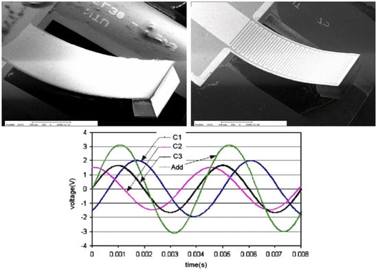
Figure 8.
SEM images of piezoelectric MEMS generator in {3–1} mode (left upper image) and {3–3} mode (right upper image), and the electrical output of three cantilevers arranged in an array and connected in series to each other (down) [41].
The integration of MEMS piezoelectric energy harvesting elements into wearable devices presents exciting prospects for self-sustaining electronics. These devices can power smart textiles, health monitoring systems, and IoT gadgets, offering a seamless and continuous energy supply without the need for external charging. Using a flexible foil as a substrate for MEMS piezoelectric energy harvesting offers several advantages in certain applications. One primary reason for choosing a flexible foil over other substrates, such as rigid materials or MEMS structures, is the ease of fabrication and flexibility in design. Flexible foils are lightweight and cost-effective and can be easily integrated into various wearable and flexible electronics without compromising comfort or mobility. Additionally, flexible foils provide a larger surface area for piezoelectric elements, allowing for higher energy generation capabilities compared to miniaturized MEMS devices [42,43]. This increased surface area enhances the efficiency of energy harvesting from mechanical vibrations, deformations, or other sources of mechanical stress (Figure 9).

Figure 9.
Image of flexible piezoelectric energy harvesting with Ga-ZnO piezoelectric materials on a seed polymer layer (left), morphology of the nanostructured Ga-ZnO grown on the seed layer (middle), and increased piezoelectric voltage of the nanostructured piezoelectric film grown on a polymeric seed layer, as compared to metal electrode (right) [44]. Reprinted from Microelectr. Eng., M. Aleksandrova, Copyright (2020), with permission from Elsevier.
3. Low-Power Electronic Converters
3.1. Single-Phase Rectifiers
In this section, various types of voltage rectifiers are considered, which are used as input stages in low-power AC-to-DC converters. The review begins with the well-known circuits of the half-wave rectifiers and bridge rectifiers or full-wave rectifiers since all other electronic circuits of this class are obtained from them. Furthermore, they serve as basic circuit configurations and are used in most cases when performing comparative analysis.
3.1.1. Half-Wave Rectifier
The basic analog circuit that can be used to rectify an AC input voltage is shown in Figure 10 [45,46]. This circuit contains a rectifier diode D and a capacitor C, with an external load connected in parallel with the capacitor. According to the Thévenin’s theorem, the input signal is represented as an input voltage source and internal resistance . Provided that no load is included in the output of the circuit, the capacitor C is charged during the positive half-cycle to a peak value equal to , where is the voltage in the forward direction of the diode, and for Si diodes, the typical values are from 0.6 to 0.7 V, while for Schottky diodes, the typical values are from 0.3 to 0.4 V. The voltage is the peak value of the input voltage, provided that no load is connected to the output because when an external load is connected, due to the influence of the internal resistance of the input signal source, the voltage value can be reduced. For the negative half-wave of the input voltage, the peak value of the voltage across the diode is equal to .

Figure 10.
Circuit diagram of a half-wave rectifier and basic waveforms of the current and voltage.
When a load with resistance is connected to the output of the rectifier, the value of the output voltage changes because the capacitor C will discharge while the diode is reverse-biased. Only during the time intervals when the input voltage is greater than the output voltage of value , the current flows from the source to the capacitor, and it is recharged. In this case, provided that the capacitor is of a sufficiently large value, the output voltage is determined by the following formula: [46]. Therefore, the value of the output voltage can be significantly reduced when a load is turned on, especially when the internal resistance of the source is relatively large.
The ratio between the DC component of the rectified current (the average value of the current ) and the output current with the load on is found as follows. Assuming that the diode is an ideal element, the curve of the current in the time intervals in which the diode is forward-biased has a sinusoidal waveform, and the repetitive peak current [47] is obtained as follows:
Also, based on the value of the output voltage, the average value of the output current is found by the formula ; then, the relation between the DC component of the rectified current and the repetitive peak current through the diode is . In this case, the average value of the rectified current is relatively small and depends on both the internal resistance of the source and the resistance of the load.
Therefore, the relatively simple structure with a small number of elements should be defined as an advantage of the basic circuit. A disadvantage of the circuit is that due to the relatively small value of the ratio of the time intervals of charge and discharge of the capacitor, the output voltage can often be obtained with a small value, even for small values of the current through the load, which is essential for energy harvesting sources providing small input power of the input signal.
A modification of the basic circuit is shown in Figure 11 [47,48]. In this circuit, two Schottky diodes are used, and for the positive polarity of the input voltage , capacitor C is charged through a diode and resistor R. For negative polarity of the input voltage, the diode is turned off, and the capacitor through the diode provides the output voltage over the load :
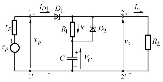
Figure 11.
Circuit diagram of a basic half-wave rectifier with two Schottky diodes.
The maximum value of the voltage to which the capacitor can be charged for the positive half-cycle of the input voltage is
where the is the voltage between the anode and cathode over the diode , and is the voltage over the .
In view of the practical usability of the circuit, the resistance value of the can be determined by the following formula [48]:
where is the maximum initial value of the input current for the present small piezoelectric thin-film harvester.
3.1.2. Bridge Rectifier
A smaller value of the ratio between the recharge and discharge time intervals of the capacitor C as well as a larger average value of the rectified current can be obtained for the bridge rectifier, given in Figure 12. This circuit is a bridge, in the branches of which four rectifier diodes are connected [25,46]. One diagonal of the bridge is connected to the input source of the signal, and the other diagonal is connected to the grounded load of the rectifier. The diodes are connected in such a way that during each half-cycle two of them operate simultaneously—the diode with the most positive anode potential ( or ) and the diode with the most negative cathode potential ( or ). As a result, the current through the load flows in the same direction. The positive pole of the rectifier is obtained at the common point of the cathodes of the diodes ( or ), and the negative pole—at the common point of the anodes of the diodes ( or ). During the recharge time interval of the capacitor C connected in parallel with the load , the positive terminal of the input source is connected to the output and the negative terminal to the ground. The input signal source can be for example the ABT-441-RC Piezo Element or ABT-448-90-RC Piezo Element, as for ABT-448-90-RC the additional wire (marked in blue) can be connected to the ground. In this way, a reduction in parasitic common-mode voltages that would occur on the load can be ensured.

Figure 12.
Circuit diagram of a bridge rectifier.
For the output voltage of the circuit, with no load connected at the output of the circuit in Figure 6, the following can be written [46]:
It can be seen from the above formula that the output voltage will be smaller compared to the value of the basic circuit (Figure 10), but when using Schottky diodes for the circuit, in some cases, this reduction can be neglected.
When connecting a load with resistance in the output port, the voltage decreases because the internal resistance of the source and diodes is taken into account. The value of the output voltage for a capacitor C of infinitely large capacitance can be determined as follows [46]:
As can be seen from Formula (12), at a larger load, i.e., with a smaller value of , the output voltage decreases. This results in a longer time interval for recharging the capacitor. At a periodic input signal with equal peak values, a steady-state operation is reached, with the incoming charge equal to the outgoing charge. In comparison with the basic circuit (Figure 10) in the bridge rectifier, due to the way of connecting the diodes, the voltage drop arising from the internal resistance of the input source is twice as small when connecting a load. As a result, there is less variation in the output voltage when the load changes. This is especially important in cases with higher internal resistance of the source .
During each time interval of recharging the capacitor, a current flow occurs with a peak value, according to Ohm’s law, equal to
After substituting Formula (12) into (13), the following is found [46]:
The maximum average power that can be obtained from a piezoelectric element is found at half the no-load rectified voltage [24,25]:
In comparison with the basic circuit in the bridge rectifier, the peak current value is smaller by a factor of . However, for both rectifier circuits, the internal resistance of the signal source has a significant effect on the peak current value. This means that a relatively high internal resistance, which at the same time changes its value, in some cases, can lead to a decrease in the current through the load. Examples of Si diodes that can be used to implement the basic and bridge rectifier circuits are 1N4148 and 1N914 (from Vishay Semiconductors® (Malvern, PA, USA)). Also, to obtain a smaller voltage drop across the diodes, Schottky diodes such as the BAT17-04, BAT54S, BAT81S, or BAT83S (from Infineon Technologies® (Neubiberg, Germany)) can be used.
Due to its superior performance, the single-phase bridge circuit is one of the most commonly used rectifier circuits and is preferred in many cases where there is no obstacle to its use. In addition, there are a large number of example circuits that partially or fully use the bridge rectifier circuit [49,50,51,52,53]. For some circuits, the bridge rectifier is partially used to form AC-to-DC electronic converters [24,50,51,53].
In cases where the voltage vp(t) generated by the piezoelectric element is not of sufficiently high amplitude, a technique in which an electronic switch (implemented with a single or a pair of MOSFETs) is connected in parallel to the input port of the voltage rectifier (Figure 13a) is used [54]. As can be seen in Figure 13b, when the signal produced by the piezoelectric generator as a result of mechanical vibrations reaches, for example, its maximum value, the electronic switch is closed for a short time interval (for example, for a time interval that is about one-hundredth of the period of the vp(t)), and the voltage decreases to zero. After this time interval, the switch is opened again, and the voltage again starts to vary according to the waveform of the voltage generated by the piezoelectric element. In this case, if proper control of the electronic switch is provided, so that exactly for the maximum and minimum values of the generated voltage, a control signal is provided to close the switch, as well as to ensure a sufficiently short interval of the closed state, the amplitude of the voltage that will be periodically applied to the input of the rectifier can be approximately twice-increased. Moreover, it is noticeable that the resulting AC voltage is distorted and delayed in phase with respect to the generated one based on the vibrations. An example block diagram for automatic self-powered switches can be found in [55]. As such, a “self-powered” switch means that the control circuit of the electronic switch is powered by the output DC voltage, i.e., by the voltage across the energy storage element.
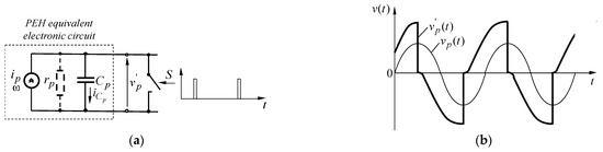
Figure 13.
Functional circuit of a piezoelectric element with additional switch, connected in parallel: (a) circuit variant; (b) timing diagrams of the voltage drop over the switch.
Based on the proposed technique with an additional electronic switch, a modification is presented in [56] in which an inductor is added in series to the switch (known as SSHI (synchronized switch harvesting on inductor)). In this way, signal distortions can be reduced (the first harmonic component is v(1)p(t)), as shown in Figure 14, allowing a further increase in the efficiency. For the time interval when the switch is closed, the system of equivalent current source ip(t), the capacitor Cp, and the inductor Ls form an oscillator. When the switch is opened, the oscillations decrease in a pseudo-periodic process.
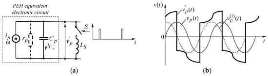
Figure 14.
Functional circuit of an SSHI: (a) circuit variant in which an inductor LS is added in series to the switch; (b) timing diagrams of the piezoelectric voltage when no load is connected.
To reduce the voltage drops across the diodes and increase the efficiency of the bridge circuit (Figure 12), MOS transistors can be used instead of diodes [8,51], as shown in Figure 15. Thus, for the circuit in Figure 15, a voltage drop across each of the transistors of up to several tens of millivolts can be achieved. The electronic circuit is made of two nMOS transistors and two pMOS transistors, and like the circuit with diodes, for each half-cycle of the input voltage ep(t), two of the transistors are in a linear mode of operation, and the other two are turned off. For example, for the indicated polarity of the input voltage ep(t), a positive voltage is supplied to the gate of M3 and a negative voltage to the gate of M1. For the same polarity, voltages are applied to the gates of M2 and M4, for which they are turned off. At a negative polarity of the ep(t), transistors M2 and M4 operate in linear mode, while M1 and M3 are turned off. Typical representatives of discrete nMOSFETs and pMOSFETs suitable for building voltage rectifiers are BSS138 and NTR1P02L (from ONSEMI), respectively.

Figure 15.
Circuit diagram of a bridge rectifier employing MOS transistors.
A further increase in energy efficiency can be achieved by connecting the piezoelectric generator in the secondary diagonal of an H-bridge with four MOS transistors working as electronic switches, using a combination of pre-biasing and synchronous charge extraction [57]. The simplified circuit diagram of such a converter is shown in Figure 16. As can be seen in Figure 16, the inductors L1 and L2 are connected in series to the transistors M1 and M2 with additional pairs of diodes. Thus, the transistors are controlled as follows: M1 and M4 provide current through inductor L1, and then M2 and M3 provide current through inductor L2. The voltage of the secondary diagonal is supplied to the electronic switches implemented with transistors M5 and M6. In this case of converting the mechanical vibrations, the resulting electrical voltage obtained can be approximately twice as high as the voltage obtained by the standard bridge rectifier (Figure 12). The output DC voltage is obtained by algebraically summing the currents at the drains of the M5 and M6 and regulating with a step-down DC-DC converter.
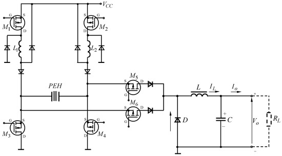
Figure 16.
Simplified circuit diagram of a pre-bias H-bridge.
3.2. Voltage Multipliers (Doublers and Quadruplers)
For thin-film piezoelectric micro-power harvesters, rectifiers with voltage multiplication are often used instead of the electronic circuits described above. At these rectifiers, in addition to rectification, a voltage increase is obtained by appropriately connecting groups of diodes and capacitors [48,58,59]. Moreover, for components with ideal electrical parameters, the amplitude of the input voltage is increased by an integer number of times; therefore, they are called rectifiers with voltage multiplication. Depending on the topological structure of the circuit, there are various types of multipliers. For the implementation of interface circuits connected to piezoelectric harvesters, single-phase asymmetric multipliers are most suitable, where the signal source and the load have a common connection node, which allows their simultaneous connection to the ground.
3.2.1. Voltage Doublers
The basic circuit of a voltage multiplier is shown in Figure 17 [25,46]. For this circuit, the voltage is multiplied by a factor of two. The circuit contains two diodes (D1 and D2), which are most often Schottky due to the possibility of obtaining a smaller voltage drop in the forward mode of operation, and two capacitors (C1 and C2). The input source is represented as a current source ip with an internal resistance rp and a capacitance Cp. The frequency of the input signal is determined by the period, as T = 1/f (f = ω/2π). The magnitude of the open-circuit input voltage (in the condition that the internal resistance rp is neglected) over the piezoelectric capacitance Cp yields [25]
where is the magnitude of the input current through the piezoelectric capacitance.

Figure 17.
Circuit diagram of a rectifier with a voltage multiplication factor of two (voltage-doubler rectifier).
The principle of operation of the circuit is implemented as follows: During the first half-cycle (or the so-called positive half-period) for which the polarity of the input source is shown without brackets, the capacitor is charged through the diode to the amplitude of the input voltage—. For this polarity, the diode is in the forward mode of operation. During the next half-cycle (or negative half-period) for which the input voltage reverses polarity (signs in brackets), the diode is turned off, and the sum of the capacitor voltage and the amplitude of the input voltage is applied to it. During this time interval, the diode is turned on, and the capacitor is charged, with the capacitor transferring part of its electrical energy until a voltage equal to the sum of the input voltage and the voltage of is reached, i.e., .
For the circuit in Figure 17, the input and output voltages and currents as a function of time [14,60] are given in Figure 18. As can be seen, the shape of the output voltage is similar to the basic rectifier circuit (Figure 12), obtaining a similar ratio of the charge and discharge time intervals of the capacitors. With a larger value of the capacitors, an output voltage with smaller ripples can be obtained. Also, at a higher frequency ω of the mechanical oscillations, a decrease in the ratio can occur.

Figure 18.
Input and output voltages and currents of the voltage-doubler rectifier in Figure 6.
The maximum value of average power that can be extracted from a piezoelectric element for the circuit in Figure 17 is found at half the no-load rectified voltage [25]:
The comparison of Formulas (15) and (17) shows that the average values of the maximum power that can be obtained from a piezoelectric generator are equal, but they are obtained at different values of the rectified voltage . For the doubler circuit, the voltage is higher and the current is smaller. A lower current flow for the voltage-doubler circuit also determines a lower power dissipation on the rectifier diodes. Furthermore, the voltage-doubler circuit uses two diodes instead of four as in the bridge rectifier circuit, which further reduces the total value of the power dissipation. An advantage of the bridge circuit compared to the voltage-doubler rectifier is the possibility of obtaining smaller ripples in the output voltage shape, which is determined by the specifics of the structure and the principle of operation.
3.2.2. Voltage Quadruplers
In cases where a higher output voltage is required, multipliers with a larger multiplication factor are used. Figure 19 shows a circuit diagram of a voltage quadrupler [45,60,61]. Compared to the voltage-doubler circuit, the voltage-quadrupler circuit results in a lower energy efficiency value because it contains a larger number of passive components.
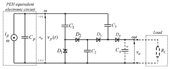
Figure 19.
Circuit diagram of a rectifier with a voltage multiplication factor of four (voltage-quadrupler circuit).
The principle of operation is similar to that of the circuit given in Figure 17. For the third half-period (the polarity of the input voltage is without brackets), the diode is turned on and the is recharged to voltage . The capacitor is also charged through the diode up to the voltage [45]
In the same time interval, the is turned off, and the voltage drop of the is applied over it, as a reverse voltage, with the value . During the fourth half-cycle (the polarity of the input voltage is in brackets), the capacitance is recharged up to and the capacitor is charged through the capacitor and the diode up to voltage .
For the implementation of electronic circuits of voltage multipliers intended for thin-film alternative sources of energy, Schottky diodes are basically used, with a voltage drop between the anode and cathode in the forward mode of operation below 200 mV at a current of up to about 1 mA. Moreover, the total power dissipation obtained is not greater than 300 mW. Examples of Schottky diodes suitable for certain types of electronic circuits are PMEG3002TV and PMEG3015EV from Nexperia® (Nijmegen, The Netherlands), NSR1020MW2 from ON Semiconductor® (Phoenix, AZ, USA), FM130EG from NXP Semiconductors® (Eindhoven, The Netherlands), and BAT54 (BAT54A, BAT54C, or BAT54S) from Nexperia®. Some of the exemplary diodes are single in a package, while others are two in a package, which may facilitate use in wearable electronic devices. When the Sthe input voltage is of a larger value (more than 2 V), Schottky diodes can be used, which have a larger voltage drop in the forward direction, such as 1N5817 and 1N5818. For them, the forward voltage has a typical value of about 500 mV, as the maximum value of the average forward rectified current is 1 A.
The capacitors are determined by the specific operating conditions, depending on the type of input signal source and the load. In this case, the total charge and discharge current flows through each of the capacitors. In this case, the last capacitor has the smallest current, and the first capacitor has the largest current. Due to the small voltage ripples , it can be assumed that the following expression applies to each capacitor [45]:
where is the charging time interval of each capacitor.
The output voltage ripples (or fluctuations) should not be relatively large, and a typical value should not exceed 5% [60] of the nominal DC voltage for a given load. From a constructive and technological point of view, it is convenient for all capacitors to have the same values, and their capacity can be determined as follows [45]:
at k = 4.
3.2.3. Maximum Point Power Tracking
As shown in Formula (34), to drain the maximum possible power from the piezoelectric generator, it is necessary to match the impedances of the generator and the load. Normally this is achieved by implementing the MPPT (Maximum Point Power Tracking) control technique, often in the DC-DC stage. When the impedance of the piezoelectric generator is considered real (active resistance), this can be easily implemented [13]. In some cases, the impedance of the piezoelectric generator could be a complex number [62]. In order to compensate the generator, an inductance connected in parallel could be used, but the value of this inductance could reach some tenth of Henrys. Such large inductance is highly recommended to be avoided in wearable electronic devices due to the practical realization considerations. There are some works discussed in detail in [62] that show possible techniques to solve this problem. The common solution is to use a small inductance with a switch and a suitable control algorithm. The common solution is to use a small inductance with a switch and suitable control algorithm. In Figure 17, one of the possible solutions is shown. It is the so-called synchronized switch harvesting on inductor (SSHI). In the presented case, the inductor is connected in parallel with the piezoelectric element. A series connection is also possible.
The SSHI is used to optimize the energy extraction from the piezoelectric generator. The theory of operation in this circuit is complex and well described [63]. In general, a switching synchronized with the mechanical vibrations of the generator is used in order to extract the maximum power from the source.
3.3. Switching DC/DC Regulators
To reduce output voltage variations due to input voltage changes or load current fluctuations, voltage regulators or so-called DC/DC (or DC-DC) regulators or converters are often connected after the rectifiers. In general, voltage regulators can be thought of as controllable series resistances that are connected in series to the load. More specifically, voltage regulators are electronic devices designed to regulate the DC power of the input source after the rectifier by the methods of pulse-width modulation (PWM) or frequency modulation (FM). Regardless of the type of modulation used, the output voltage can be of a value greater or less than the input voltage after the rectifier. The regulators for which the output voltage level is less than the input voltage are called buck regulators (or step-down converters), and the regulators for which the output voltage level is greater than the input voltage are called boost regulators or (or step-up converters) [52,64,65,66].
In the realization of control circuits for low-power stand-alone regulators designed to extract electrical energy from piezoelectric generators, the regulation of DC power using PWM is used relatively more often. Implementing control circuits with the application of PWM allows lower power dissipation with a smaller number of passive and active components and at a lower frequency of the pulse oscillator. In some cases, the input AC voltage obtained from the piezoelectric generator is also used as a rectangular waveform of the signal for controlling the duty cycle, i.e., the intervals during which the series resistance has a small and large value are obtained by an additional latching circuit. A functional diagram [46] of a voltage rectifier with a DC-DC converter or PSD intended for extracting electrical energy from piezoelectric generators is given in Figure 20. As can be seen in Figure 21, after the rectifier or voltage multiplier, the series-controlled resistance can be replaced by a switching circuit that uses a bipolar or MOS transistor operating as an electronic switch. This switch produces a pulsating voltage whose average value varies from zero to approximately the amplitude of the input voltage depending on the duty cycle δ. After the switch, a low-pass filter is usually included, which reduces the ripples of the output voltage. The PWM controller is an electronic device that compares the output voltage with a set reference voltage and produces a control pulse signal with a variable duty cycle. For example, if , then a signal with a larger duty cycle is received at the output terminal of the regulator, i.e., the time interval during which the switch is closed increases. In this case, the frequency f of the control pulse signal remains constant. In cases where the input voltage is used as feedback (dashed line) to change the duty cycle, the output DC voltage forms the supply voltage of the active components in the PWM controller.
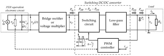
Figure 20.
Functional diagram of a rectifier with DC-DC regulator (or PSD), intended for extracting electrical energy from piezoelectric generators.
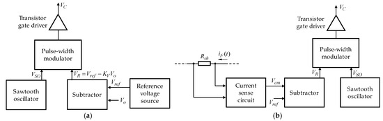
Figure 21.
Block diagram of a PWM controller: (a) circuit variant using output voltage as a feedback signal; (b) circuit variant using piezoelectric input current as a feedback signal.
One of the basic electrical parameters of the DC-DC converter is the overall electrical energy efficiency (or power conversion efficiency), which can be calculated based on the measured values of the average currents at certain nodes:
where is the power of the extracted input signal and is the output power of the circuit ( is the output power after the low-pass filter and is the power consumption of the PWM controller).
The losses in the switching circuit and the low-pass filter as well as in the PWM controller versus the power received by the piezoelectric element can be determined by and , respectively.
Additionally, for the DC-DC converter, the efficiency of the circuit configuration used is evaluated by a figure of merit (FoM). The FoM parameter is defined as the ratio of the power that can be delivered from the storage element (rechargeable battery or ultra-capacitor) to the maximum average power that can be obtained from the piezoelectric element, provided that there is a lossless rectifier () [7]:
Although miniaturized single piezoelectric generators can provide a higher voltage (>10 V) from mechanical vibrations compared to electrostatic and electromagnetic generators, the current that can be obtained is of relatively small value (<0.1 mA), and as a result, the electrical power will also be of small value (with typical values from 10 to 100 μW). Then, a value greater than unity can be obtained for the FoM parameter if a rechargeable battery or a supercapacitor is connected to the output port of the DC-DC regulator. Thus, the instantaneous value of the electrical power that can be obtained from a charged battery or supercapacitor can be significantly greater than the output power of the same DC-DC converter even with minimal power dissipation in the bridge rectifier or switching circuit.
The electrical energy that spreads from the input to the output of the power source with an energy storage element (supercapacitor) connected to the output is determined as follows [7,8]:
where is the capacitance of the energy storage element, is a function depending on the type of voltage rectifier selected and its circuit parameters, and is the output voltage of the rectifier over the filter capacitor C (see Figure 15 and Figure 17) (voltage fluctuations typically do not exceed 5% of the nominal dc value).
Then, the charging efficiency can be calculated as the ratio of the energy that is transferred to the output to the energy that is generated by the vibrations [7,8]:
Based on the functional diagram (Figure 20) in Figure 21a,b, block diagrams of PWM controllers are presented depending on the way of obtaining the feedback signal. In cases where the output DC voltage is used as the input signal to the feedback network for the PWM controller, the block diagram [46,60] in Figure 21a is obtained. In it, the output voltage is initially subtracted from the reference voltage , with previously being multiplied by a factor , which is less than unity. The output voltage of the subtractor is applied to one input terminal of a PWM, while a voltage from a sawtooth oscillator is applied to the other input terminal. As a result of the comparison of the two voltages at the output of the PWM through the transistor gate driver, a control signal with a rectangular shape and a variable duty cycle is obtained, depending on how much the voltage is greater than the triangular voltage , produced by the sawtooth oscillator (Figure 22). The time during which the switch is closed is as long as the time interval . With a longer duration, the switch is closed for a longer time; this increases the average value of the output voltage as well.
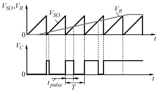
Figure 22.
Input and output voltages of the PWM comparator (Figure 21a).
In cases where the current after the rectifier is used as an input signal to the feedback circuit of the PWM controller, the block diagram in Figure 21b is obtained. To obtain a control signal, the is passed through a shunt resistor indicated with . A small voltage drop is obtained over the , which is amplified by an amplifier circuit, for example, with a micro-power op-amp. For the output voltage, is obtained. This voltage is compared to the reference voltage, yielding the voltage , which is applied to one of the two inputs of the modulator. The voltage from the sawtooth generator is applied to the other input.
3.3.1. Structure and Operational Principle of Step-Down Converters
A simplified circuit configuration of a step-down converter is given in Figure 23. In this circuit, the output voltage can take values depending on the value of the duty cycle, and the switch S is represented as an ideal element, with zero resistance in the closed state and zero current when open. Additionally, the circuit contains a diode D (most commonly a Schottky diode, such as those proposed in the previous section), a coil L, and a smoothing capacitor C. When switch S is closed, the current through coil L increases as capacitor C charges with the polarity shown in the figure. When it opens, the current through the coil retains its direction, and the diode is turned on. The current through the coil decreases, and the voltage across the capacitor decreases until the switch closes again. The voltage and current timing diagrams illustrating the principle of operation of the converter are shown in Figure 24.
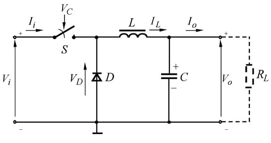
Figure 23.
Simplified circuit configuration of a step-down converter.
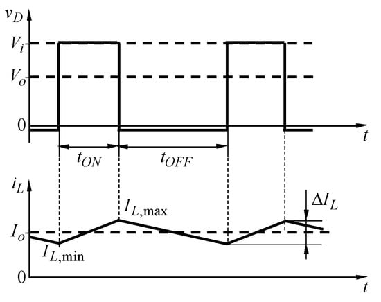
Figure 24.
Voltage and current timing diagrams of a step-down converter.
Since the coil encloses an alternating magnetic flux, a voltage is induced in it, which has the form [46]
The negative sign reflects Lenz’s rule, according to which the induced voltage has such a direction as to oppose the change in current.
When the switch in the circuit shown in Figure 23 is closed (or during the ON-time interval), the voltage drop across the coil is , while when the switch is open, (or during the OFF-time interval), the voltage is .
By using (25), for a linearized current approximation, the following is obtained at the switching moment:
Then, based on the above expression, the following is obtained for the output voltage value [46]:
where is the period of the control signal, as the time interval coincides with the duration of the pulse during which the switch is closed.
The value of the output current is determined by the average value of the current through the coil, or is obtained for the current.
The inductance of the coil is chosen to be as large as possible so that when the switch is open current values below the minimum value (in which the current through the coil reaches zero during the time interval when the switch is open) are not reached [15,32]:
3.3.2. Structure and Operational Principle of Step-Up Converters
A simplified schematic configuration of a step-up converter is given in Figure 25, and timing diagrams of voltages and currents are given in Figure 26. In this circuit, when the switch is open, a current flows through the coil, inducing a voltage. When the switch is opened, the direction of the current is retained, and the output voltage is equal to the sum of the input voltage and the voltage across the coil. As a result, the output voltage is greater than the input voltage.
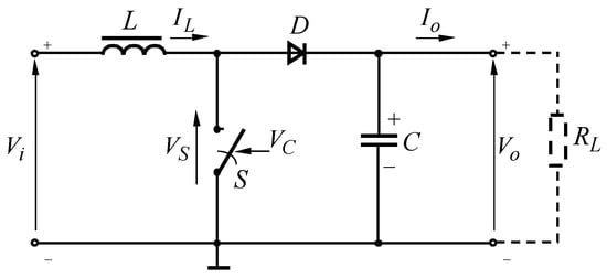
Figure 25.
Simplified circuit configuration of a step-up converter.
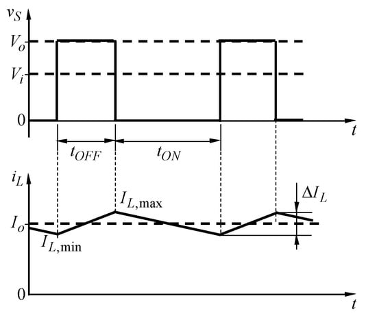
Figure 26.
Voltage and current timing diagrams of a step-up converter.
The output voltage value is found similarly as for the previous circuit, having the form [46]
According to the formula in [15,66], to determine the value of the coil, the following expression is obtained:
4. Conventional Parallel-Plate Capacitors and Thin-Film Supercapacitors—Equivalent Circuits and Basic Parameters
Based on the analysis presented above, piezoelectric elements that are suitable for sources (or generators) of electrical energy from spontaneous mechanical vibrations can be considered as current sources with a relatively large internal resistance. Moreover, mechanical vibrations in most cases cause voltages with a non-sinusoidal waveform, which lead to relatively complex analytical expressions for the electrical parameters. Under these operating conditions, to ensure the continuous operation of the electronic devices that use the produced voltage of the piezoelectric element as a power supply voltage, it is necessary to ensure the possibility of storing the electrical energy before it is applied to an electronic converter and load. This means that directly after rectifying the AC voltage produced, an inductor or capacitor can be connected. The inductors are used less often since at a large value of the inductances they have a relatively complex construction and, in some cases, are relatively large in size. Also, inductors are more difficult to implement in integrated circuits. Moreover, when environmental parameters change, inductors more easily change their electrical parameters. In most practical cases, conventional parallel-plate capacitors with a relatively large capacity with a small value of equivalent series resistance (ESR) or supercapacitors are used, as thin-film electronic elements are preferred for wearable electronic devices. Also, when using supercapacitors as energy storage elements, to limit the voltage across them, a limiter is connected in parallel, most often implemented with a Zener diode, whose anode is connected to the ground. To ensure the completeness of the review, this section of this paper presents an analysis of the structure, principle of operation, and basic parameters of conventional parallel-plate capacitors and thin-film supercapacitors, which are suitable for use as energy storage elements in wearable electronic devices.
4.1. Conventional Parallel-Plate Capacitors
Parallel-plate capacitors are a system of two conductive bodies—electrodes—separated by a dielectric. The two electrodes have equal magnitude charges with different signs, where Q1 = Q and Q2 = −Q. Thus, the capacitance is defined as the ratio of the stored charge Q and the voltage v between the electrodes [67]:
For a parallel-plate capacitor, the capacitance depends on the geometric dimensions of the electrodes and on the absolute permittivity. In principle, the structure of a parallel-plate capacitor is given in Figure 27. In it, the deformation of the electric field at the edges is neglected, and the distance between the electrodes is d, the value of which is significantly smaller compared to the transverse dimensions. In this case, the electric field in the interelectrode space has a uniform character with an electric intensity of constant value (E = const), and outside the capacitor, there is no electric field. Then, for the closed surface, shown in Figure 10 with a dashed line based on Gauss’s law of electric intensity, the following is obtained:
where ε is the absolute electrical permeability of the insulating material (ε = × , where is the vacuum permittivity and is equal to 8.854187… × 10–12 F/m, and is the relative dielectric permittivity (or effective permittivity), indicating how many times the force of interaction between two charged bodies is reduced if the space between them is not a vacuum but is filled with a corresponding material), and A is the area of the electrodes.

Figure 27.
Simplified structure of a parallel-plate capacitor.
Then, the voltage between the electrodes (1 and 2) is defined as the circulation of the electric intensity vector between the two points along the path l:
where the designation 1l2 indicates that the circulation of the vector depends not only on the endpoints 1 and 2 but also on the selected circulation loop.
With Formula (31), the capacitance of the parallel-plate capacitor in the presence of geometrical symmetry of both electrodes is determined as follows:
As can be seen from Formula (34), two of the parameters have a constant value, where is the dielectric constant in vacuum and is the dielectric constant depending on the material contained between the electrodes. As a result, an increase in capacity can be obtained under the condition of changing the type of material between the electrodes and increasing their area. Also, a larger value of the capacitance of the parallel-plate capacitors can be obtained by reducing the thickness of the electrolytic dielectric between the two electrodes.
At a larger value of the capacitance, a larger value of the stored electrical energy WC can be obtained, i.e.,
where .
The electrical power P of a capacitor is defined as the energy delivered per unit of time. In order to determine the maximum power that can be delivered to a given load , Figure 28 shows the equivalent series diagram of a parallel-plate capacitor with internal resistance , which is connected to the load. In this case, the power P of the load at a voltage resonance () has the form [25]
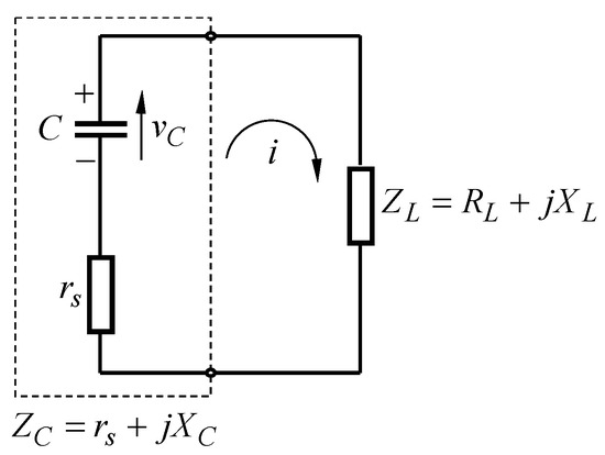
Figure 28.
Equivalent series circuit of a parallel-plate capacitor with a given active load .
The maximum value of the power is determined by calculating for which value of the first derivative is equal to zero:
The first derivative is set to zero for , which yields
As can be seen from Formulas (34) and (35), parallel-plate capacitors can deliver a relatively large amount of energy in a short time, but the energy density is less compared, for example, to rechargeable batteries. Although capacitors have a lower energy density, their volume or mass is also relatively smaller than that of batteries, and they can quickly discharge in a short time. Exemplary commercially available polymer aluminum solid electrolytic capacitors up to 1000 μF with a low ESR value for pulse signals are Fujicon® Electric Company’s MA [68] and FZ [69] series, as well as Yageo®’s AC [70] series.
4.2. Thin-Film Ultra-Capacitors (or Supercapacitors)
To increase the energy density while maintaining a relatively small mass and volume in portable alternative energy sources, capacitors with high and even ultra-high capacitance are used, or ultra-capacitors, sometimes called “supercapacitors” [71,72]. In comparison with parallel-plate capacitors, supercapacitors use the same principle of operation described above; however, they are characterized by a larger area that allows a greater density of charges, and they also have thinner dielectric layers. As a result, a larger capacitance value is achieved for supercapacitors compared to parallel-plate capacitors. The most commonly used supercapacitors (Figure 29) are based on electrochemical double-layer capacitors (EDLCs) [73,74,75,76]. When an AC voltage is applied between the two electrodes, the ions in the bulk or on the electric double layers diffuse through the separator or separators to the oppositely charged electrode. Moreover, the electrodes are designed to limit recombination processes at the surface of the electrodes. For the supercapacitors, the specific capacitance CS and the areal capacitance CA can be found as follows [71]:
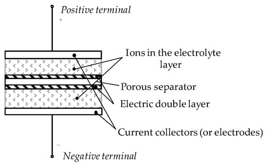
Figure 29.
Simplified structure of an electrochemical double-layer capacitor.
Currently, for the realization of thin-film supercapacitors, MXenes are widely used, which are 2D layered transition metal carbides or carbonitrides exfoliated from their parent MAX phases by selective wet chemical etching processes [77]. Furthermore, MXene supercapacitors as electrochemical energy storage devices ensure high power density, high charge/discharge efficiency, and long duration of the real devices [78,79,80].
Often, when using thin-film supercapacitors, the capacitance of a single element is not sufficient, and then up to n number of capacitors are connected in parallel, while the voltage drop across each of them remains the same. In the general case, for n number of capacitors, the total state of charge has the form
Then, the equivalent capacitance will be obtained from the individual capacitances connected in parallel, i.e.,
For comparison with the parallel-plane capacitors, an effective power density parameter is defined for the supercapacitors. This parameter is defined as the power density per unit of volume or galvanometric power density per unit of mass. The maximum value of the galvanometric power density is determined for the instantaneous power delivered at the full rated voltage Vc,max with an internal equivalent series resistance rs specified at a certain frequency [71]:
The analysis of various literature sources shows that for the purposes of the design process, considering the specific structure, the equivalent electric circuits of supercapacitors can contain RC groups (or RC branches) connected in parallel. Moreover, the individual branches, which have an active–capacitive character, have different time constants. The electrical double layers of the individual separators in the multilayer structure create an additional interfacial tension, in which the capacitance between the external electrodes depends on the potential difference. With a certain approximation, in the formula for the capacity, the component is also obtained, which depends linearly on the applied voltage. Based on the generalized structure in Figure 29, as well as the equivalent circuits given in [75,76,77], Figure 30 shows an example equivalent circuit that can be used as an EDLC replacement circuit. The first RC group contains resistance R1 and capacitance C1, which changes its value depending on the value of the applied voltage v1. The second and third RS groups have an increasing time constant, modeling the interface between two materials at different phase delays. The resistance R4 models the leakage current, and the inductance L1 models the parasitic inductance of the terminals. In most cases, this inductance can be neglected as it has a small value of up to 100 nH. Some recommendations for determining the values of the model parameters can be found in [75,76].
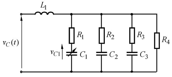
Figure 30.
Equivalent electrical circuit of an electrochemical double-layer capacitor.
Based on the principle of operation of capacitors, the following expression applies to the dependence of the capacity C1 [75]:
where has a constant value and is a coefficient with dimension F/V.
5. Comparative Analysis of Vibrational Energy Harvesting Systems
Based on the analysis of the principle of operation of basic electronic circuits suitable for operation with piezoelectric generators and a review of circuit configurations reported in the literature, Table 1 and Table 2 summarize the electrical parameters of selected low-power-supply devices. More specifically, Table 1 represents self-supplied energy harvesting circuits and their electrical parameters reported before 2018, and Table 2 shows published circuits from the last five years. Moreover, these electronic circuits were chosen because their circuitries include interesting and useful design techniques that lead to improved energy efficiency on the one hand and can serve as a basis for developing new circuit configurations. On the other hand, all the circuit variants presented are self-powered by a signal generated by a piezoelectric element, and for most of them, a low-power rechargeable battery or supercapacitor can be connected to their output port. In comparison with the standard batteries, an advantage of using low-power rechargeable batteries or supercapacitors is that they do not need to be changed often, as in many cases these operations are impossible or too expensive, especially when a large network is built of electronic devices with multiple connections between them. A disadvantage of low-power rechargeable batteries and supercapacitors is that, due to their smaller size, they are more easily depleted. Furthermore, in most cases, a relatively complex electronic circuit has to be designed for them to charge the energy storage elements by converting the energy from the input source, as well as to have functions to track their discharge. In many cases, regardless of the inexhaustible possibilities of harvesting energy from the environment, the recharging property of the energy storage elements can be limited as a result of changing the operating conditions of the piezoelectric generator or changing the magnitude of the consumed current. Independently from the mentioned disadvantages, obtaining electrical energy from the environment, on the one hand, is relatively inexpensive and environmentally friendly, but on the other hand, more importantly, obtaining energy from motion or electromagnetic radiation helps to avoid the use of a bulky “tank” that, for example, standard high-capacity batteries require.
The analysis of the summarized parameters in Table 1 and Table 2 shows that for the implementation of a PSD, application-specific integrated circuits or commercially available integrated circuits, which maintain a large number of functional capabilities, are increasingly used. There are fewer electronic circuits implemented with discrete elements since for them, in most cases, the power dissipation is obtained with a comparatively larger value, and a smaller value for the energy efficiency is obtained. However, in all cases, the maximum overall electrical energy efficiency ranges from 50% to 80% and only in some cases exceeds 85% [8,81,82,83,84,85]. One of the main trends in the construction of low-power electronic converters is increasing the output power (>1 mW and mainly providing a larger output current) and simultaneously reducing the power dissipation (≤10 μW). As can be seen in Table 1 and Table 2, a higher value for electrical energy efficiency can be achieved by designing the electronic circuits basically using circuit variants of synchronized switch harvesting on inductor (SSHI) [8,81,82,83,86,87,88,89,90,91,92,93,94], voltage rectifiers employing MOS transistors [53,81,85,87,94] or voltage multipliers with Schottky diodes [7,59,60,61,84,86], active diodes [82,87,91,93], cold-start-up circuits [8,11,83,89], active and sleep mode of operation [8,81], self-powered circuits from the signal source, and providing a buck/boost DC-DC converter mode of operation [92], as well as a charging control circuit for an energy storage element. An interesting implementation of an electronic circuit for a cold start, which can determine an increase in energy efficiency, is given in [55]. Furthermore, power sources [66,90] with an energy efficiency higher than 90% are of particular interest, which is achieved basically through the optimization of the AC/DC rectification circuit. More specifically, for the system proposed in [52], the AC/DC conversion is conducted by using a low-power MOS-based rectifier, consisting of a passive negative voltage converter followed by an active diode. For the system proposed in [89], the rectification process is realized by developing an enhanced SSHI circuit in which an external inductor in the range of μH is used to flip the residual voltage on the Cp and broaden the duration of charging the storage capacitance. As a result, it can expand the delivered output power in an efficient relatively small chip area.
For the effective operation of the power sources listed above in Table 1 and Table 2, some high-performance piezoelectric generators commonly used as input sources with their more important electrical parameters (such as maximum power up to 500 μW, open-circuit voltage amplitude up to 20 V at the maximum frequency of mechanical vibrations slightly above 200 Hz for a single element) are also indicated. For each of the electronic circuits, the appropriate types of electrical energy storage elements are also indicated, which can be added to the output ports to provide the necessary constant voltage and drivable current. A higher value for the output current or a larger output power over the load in a relatively small power conversion system can be obtained by using piezoelectric elements, as shown in [7], or by connecting low-power supercapacitors in the output [11] and also implementing a group of thin-film supercapacitors (i.e., two, four, or eight samples) based on a new family of two-dimensional materials [78,79,80].
Based on an analysis of current achievements in energy harvesting systems within the framework of project BG-RRP-2.004-0005, the future work of the authors is focused on the design of micro-power supply devices that convert electrical energy from commercially available low-power piezoelectric generators to energy storage elements based on new 2D layered transition metal carbide (MXene) structures.

Table 1.
Comparison of selected self-supplied energy harvesting circuits reported before 2018.
Table 1.
Comparison of selected self-supplied energy harvesting circuits reported before 2018.
| Parameter | (Tabesh et al.) [60] | (Ramadass et al.) [86] | (Hehn et al.) [95] | (Kwon et al.) [91] | (Romani et al.) [7] | (Aktakka et al.) [8] | (Liu et al.) [9] | (Sanchez et al.) [81] | (Wu et al.) [82] | (Du et al.) [53] |
|---|---|---|---|---|---|---|---|---|---|---|
| Piezoelectric Element | ||||||||||
| Type of PEH | Q220-A4-303YB | MIDE V22B | MIDE V22B | MIDE V22B | Three cantilevered Q220-A4-303YB | Custom MEMS harvester, 27 mm3 | Custom MEMS harvester, 150 mm3 | MIDE V21B and V22B | MIDE V22B | MIDE V21BL |
| Excitation frequency | 250 Hz | 225 Hz | 174 Hz | 143 Hz | 40 Hz | 155 Hz | 4–5 Hz | 225 Hz | 144 Hz | 92 Hz |
| Maximum average power (or raw power) | >500 μW (2.3 g) | n.a. | 557 μW | 80 μW | 405 μW | 95 μW | 400 μW | n.a. | n.a. | n.a. |
| Piezoelectric capacitance | 52 nF | 12 nF | 19.5 nF | 15 nF | 52 nF | 8.5 nF | 25 nF | 26 nF | 19 nF | 45 nF |
| Open-circuit voltage amplitude | 3–20 V | 2.4 V | 12.6 V | 2.6 V | 20 V | 1.8 V | 6 V | 2.5 V | 4.9 V | 2.5 V |
| Piezoelectric material | PZT-5A4E | PZT-5H | PZT-5H | PZT-5H | PZT-5A | PZT | Micro-Fiber Composite (MFC) materials | PZT-5A and PZT-5H | PZT-5H | PZT-5H |
| Controlling circuit | ||||||||||
| Conversion circuit | Voltage-doubler rectifier; buck converter; analog controller | Diode bridge; bias flip rectifier; DC-DC buck regulator | pNVC (5); active diode; series SECE | Energy-investing switched-inductor AC-DC converter | Diode bridge; single SECE (2) for three PEHs | Bias clip stage; NVC; active diode; trickle battery charger | LTC3588-1 extraction circuit; battery charger system LTC4071 | Parallel-SSHI rectifier; DC-DC converter; LDO | SSHI circuit and an active rectifier | Diode bridge; SSHC (3) for PEH |
| Type of realization | Discrete components | Process: 350 nm CMOS; chip area: 4.3 mm2 | Process: 350 nm CMOS; chip area: 1.25 mm2 | Process: 180 nm CMOS; chip area: 2.3 mm2 | Discrete components | Process: 180 nm CMOS; chip area: 0.3 mm2 | Discrete components | Process: 350 nm CMOS; chip area: 1.17 mm2 | Process: 250 nm BiCMOS; chip area: 0.98 × 0.76 mm2 | Process: 350 nm CMOS; chip area: 2.9 mm2 |
| Power consumption | <50 μW | <2 μW | 1.7–4.7 μW | 2–3 μW | 8–18 μW | 0.5 μW (active); 10 pW (sleep) | <2 μW | 1 mW (active); 4 μW (sleep) | 11.5 μW | ≈1.7 μW |
| Output DC voltage | 7.5 V | 1.8 V | 5 V | 3.7 V | 6.5 V | 1.8 V | 1.8 V | 0.7–5 V regulated | up to 5 V | up to 6 V |
| Output power | 0.5 mW | 32.5 μW | 10–100 μW | ≈50 μW | 300 μW | 94.5 μW | 200 mW | ≈160 μW | 136 μW | 161.8 μW |
| FoM (through Equation (36)) | n.a. | n.a. | up to 3.45 | n.a. | n.a. | n.a. | up to 4.38 | 2.07 | up to 6.25 | |
| Cold start-up | Yes | No | No | No | Yes | Yes | Yes | Yes | Yes | Yes |
| Maximum overall electrical energy efficiency | 60% | 85% (4) | 85% | 69% (4) | 50–74% | 58–86% (4) | >30% | 94% | 85% | 80% |
| Start-up requirements | Self-powered; battery at the output port (1) | Self-powered; battery at the output port (1) | Self-powered; capacitor at the output port | Self-powered; battery at the output port (1) | Self-powered; capacitor 33 μF at the output port (1) | Self-powered; supercapacitor 20 mF at the output port (1) | Self-powered; battery at the output port (1) | Self-powered; storage capacitor 200 μF at the output port (1) | Self-powered; rechargeable battery at the output port (1) | Self-powered; supercapacitor 2.5 mF at the output port (1) |
| Year | 2010 | 2010 | 2012 | 2014 | 2014 | 2014 | 2015 | 2016 | 2017 | 2017 |
(1) A battery or a capacitor is connected to the output port of the PSD; (2) Synchronous electrical charge extraction (SECE); (3) Synchronized switch harvesting on capacitors (SSHCs); (4) The value is defined for a maximum charging electrical energy efficiency; (5) Passive negative voltage converter (pNVC). n.a. = data not available.
Table 2.
Comparison of selected self-supplied energy harvesting circuits, reported during the last five years.
Table 2.
Comparison of selected self-supplied energy harvesting circuits, reported during the last five years.
| Parameter | (Du et al.) [93] | (Peng et al.) [89] | (Du et al.) [88] | (Li et al.) [87] | (Chew et al.) [59] | (Chamanian et al.) [92] | (Çiftci et al.) [84] | (Chamanian et al.) [83] | (Huet et al.) [11] | (Ben Ammar et al.) [85] | (Costanzo et al.) [94] |
|---|---|---|---|---|---|---|---|---|---|---|---|
| Piezoelectric Element | |||||||||||
| Type of PEH | Custom MEMS harvester, 1.0 g | MIDE PPA1022 | Custom MEMS harvester, 1.0 g | MIDE PPA1021 and PPA1011 | 1 Smart Material MFC8528-P2 | Q220-A4-303YB | Custom MEMS harvester with a footprint of 36 mm2 | MIDE V22BL | MIDE PPA 1014 | AB4113BLW100-R | MIDE PPA-4011 |
| Excitation frequency | 219 Hz | 53–85 Hz | 219 Hz | 100–140 Hz | 10 Hz (min) | 317 Hz | 450 Hz | 208 Hz | <100 Hz | 1 Hz | 232 Hz |
| Maximum average power (or raw power) | 186 μW | n.a. | 186 μW | 160–200 μW | 3.96 μW | n.a. | n.a. | n.a. | n.a. | 4.32 mW | n.a. |
| Piezoelectric capacitance | 1.94 nF | 8 nF | 1.94 nF | 20 and 100 nF | n.a. | 2 nF | 2 nF | 4.66 nF | <55 nF | 150 nF | n.a. |
| Open-circuit voltage amplitude | up to 4.2 V | 0.85–2.13 V | up to 7 V | 1.6–2.66 V | 1.2–20 V | 1.12 V | <3.2 V | 0.87 V | <8 V | 7.2 V | <2 V |
| Piezoelectric material | N/A | PZT-5H | N/A | PZT-5H | Micro-Fiber Composite (MFC) material | PZT-5A | N/A | PZT-5H | PZT-5H | PZT | PZT-5H |
| Controlling circuit | |||||||||||
| Conversion circuit | Cold start-up SSHI interface circuit and full-bridge rectifier | Sense-and- set (SaS) rectifier with a static power of 7 nW | Split-electrode SSHC (SE-SSHC) rectifier | Parallel-SSHI rectifier; buck/boost DC-DC converter | Voltage doubler; analog control circuit LTC3388-3 buck converter and LTC2934-2 | Self-adapting synchronized-switch harvesting (SA-SSH) interface circuit | SSHC circuit utilizing a flipping inductor; DC-DC converter; LDO | Enhanced SSHI system (used external inductor in the range of μHs) | LTC3588-1 extraction circuit; balancing system ALD810023 for ultra-caps | Interface circuit for footstep | Energy Harvester Power Optimizer (EHPO) |
| Type of realization | Process: 180 nm CMOS; chip area: 0.2 mm2 | Process: 180 nm CMOS; chip area: 0.47 mm2 | Process: 180 nm CMOS; chip area: 3.9 mm2 | Process: 130 nm CMOS; chip area: 1.07 mm2 | Discrete components | Process: 180 nm CMOS; chip area: 0.6 × 0.9 mm | Process: 180 nm CMOS; chip area: 1.23 mm2 | Process: 180 nm CMOS; chip area: 0.28 mm2 | Discrete components | Discrete components | Discrete components |
| Power consumption | 0.359 μW (1) | ≈10 μW (1) | ≈2.9 μW (1) | 5 μW (1) | ≤80 μW | 1.3 μW | ≈18 μW (1) | 3.84–26.37 μW | 50 μW | n.a. | n.a. |
| Output DC voltage | 1.5 V | up to 2 V | up to 6 V | ≤3 V | ≤3.3 V | up to 4 V | ≤3 V | 2.68 V optimum value | 2.8–3.6 V | 3.6 V | n.a |
| Output power | 30 μW | 15 μW | 16.1 μW | 120–200 μW | n.a. | 3.22 μW | 24.2 μW | 3.84 μW | 213.2 mW | 4.32 mW | 2.81 mW |
| FoM (through Equation (36)) | n.a. | up to 7.8 | n.a. | 8.47 | n.a. | 4.04 | 2.62 | up to 5.23 | n.a. | n.a. | n.a. |
| Cold start-up | Yes | Yes | Yes | Yes | Yes | Yes | Yes | Yes | Yes | Yes | Yes |
| Maximum overall electrical energy efficiency | 50% | 42% | >80% | 78% | n.a. | n.a. | 83% (L = 100 μH) | 93% (L = 820 μH) | 36% | 83.33% | n.a. |
| Start-up requirements | Self-powered; storage capacitor at the output port (2) | Self-powered; battery at the output port (2) | Self-powered; storage capacitor at the output port (2) | Self-powered; supercapacitor 4.7 mF at the output port (2) | Self-powered; supercapacitor 22 mF at the output port (2) | Self-powered; capacitor 1 μF at the output port (2) | Self-powered; storage capacitor 453 nF at the output port (2) | Self-powered; storage capacitor 449 nF at the output port (2) | Self-powered; supercapacitors 8 × 1 F at the output port (2) | Self-powered; supercapacitor 1.0 mF at the output port (2) | n.a. |
| Year | 2018 | 2019 | 2019 | 2019 | 2020 | 2020 | 2021 | 2021 | 2022 | 2023 | 2023 |
(1) Calculated from the paper; (2) A battery or capacitor is connected to the output port of the PSD. n.a. = data not available.
6. Practical Realizations of Piezoelectric Power Conversion Circuits
6.1. Examples of Comercially Avaliable Monolithic Micro-Power Electronic AC-DC Converters
In the last few years, based on the systematic approaches presented in the previous section and the structure of well-known circuit configurations, various commercially available monolithic integrated circuits, such as [96,97,98], which have a relatively low power consumption and small dimensions, such as the effective area of a semiconductor chip, have been developed. Moreover, these types of integrated circuits contain functional blocks of a rectifier or voltage multiplier and a DC-DC converter, as well as some additional blocks for the charge management of rechargeable batteries or supercapacitors connected in the output port. Some of these integrated circuits also have functional stages to include an additional non-rechargeable battery (or backup primary battery), in case the input signal is of insufficient amplitude to ensure the charging of the energy storage elements connected to the output of the integrated circuit. Also, some of them include functional blocks for connection via a standard interface with a microcontroller or other digital circuit. Exemplary energy harvesters that use a monolithic integrated circuit to convert an AC voltage received from a piezoelectric generator into a DC signal for charging a supercapacitor or battery are given in [3] and [11], respectively. The analysis of the literary sources also showed the presence of electronic converters in which, instead of commercially available circuits [82,84,86,87,88,89,91,92,93], specialized integrated circuits designed for specific applications are used.
One of the popular commercially available integrated circuits that provides the conversion of mechanical vibrations from piezoelectric elements is the LTC3588-1 (from Analog Devices) [96]. The LTC3588-1 is a specialized integrated circuit designed for energy harvesting that has relatively low self-consumption and small physical dimensions. Furthermore, the internal structure of the LTC3588-1 includes some interesting microelectronic techniques that can produce a wide operating dynamic range and a relatively high value of electrical energy efficiency. As shown in Figure 31, the LTC3588-1 contains a built-in rectifier at the input after which a high-efficiency step-down converter is connected, which is optimized for operation with photovoltaics, piezoelectrics, and electromagnetic transducers. The input operating voltage is from 2.7 V to 20 V. The output voltage is digitally selectable from the fixed values of 1.8 V, 2.5 V, 3.3 V, and 3.6 V. The guaranteed output current is 100 mA. There is a digital output signal indicating at a logic high level that the output voltage is at 92% of the set value, which can be used to enable integrated circuits relying on this voltage for power.

Figure 31.
Block diagram of a low-power circuit configuration for energy harvesting using LTC3588-1 [96].
The voltage generated by the piezoelectric is rectified by the built-in diode rectifier, which has a small drop in the typical value of current from such a source (10 µA). This voltage is output to pin Vin, to which the external capacitor Cstorage (or CSTO) is connected. The voltage on it is limited by the built-in Zener diode. This voltage is used to power the integrated circuit as well as the input voltage to the step-down converter that maintains the output voltage. It is set by the digital signals D0 and D1. The output SW is the point between the two switching transistors that are part of the converter. An inductance is externally connected to it. The output voltage is monitored through a Vout pin. The voltage from this pin passes through a controllable resistor voltage divider. Its output is used to enable the buck converter, via the SLEEP comparator, and also to set the PGOOD output logic level, which indicates that the output voltage has reached the reference. The SLEEP comparator reduces switching losses because the step-down converter does not operate continuously but is enabled and disabled when the output voltage is below or above set lower and upper thresholds, respectively. Additionally, internally there is a circuit monitoring the voltage on the input capacitor, which prohibits the operation of the step-down converter if it falls below a limit set at 300 mV above the set voltage at the output.
Based on the above-described structure and principle of operation of the LTC3588-1, an experimental study was carried out to demonstrate its effectiveness and practical applicability. More specifically, in the experimental study, a DC1459B-A (from Analog Devices) development system was used. The test AC signal was obtained from a function generator type MFG-2110 with a high internal resistance equal to 10 kΩ, so as to simulate the typical behavior of a piezoelectric element. The amplitude of the signal is up to 8 V, and the frequency is set equal to 20 Hz. The experimental study was performed in two cases, for an output voltage of 1.8 V and 3.6 V, and for each value of the voltage, a study was performed with four and eight supercapacitors type HV0810-2R7105-R (from Eaton® (Dublin, Ireland)) connected in series. For both cases, the signal produced by the piezoelectric element was applied to the input terminals of the built-in voltage rectifier, having an amplitude of up to 10 V. A digital voltmeter type VC820 (from Voltcraft® (Hirschau Germany)) was used to measure the Vin input voltage (the voltage on the supercapacitors), the output voltage Vout of the converter, and the Power-Good (PGOOD) voltage, which includes an optoelectronic interface with beam waveguide technology. Since the standard interface cable has an RC232 output, an adapter cable was additionally used that converts the RC232 to USB standard to provide a connection to a personal computer. To visualize the measured voltages, an interface program VC820/840, specially developed by the manufacturer for working with digital voltmeters of the VC820 type, was used. To store the measured voltages, a built-in function was used to save arrays of data in the MS Excel® file format. As a result of the experimental study, Figure 32 and Figure 33 present the timing diagrams of the input voltage Vin obtained over several supercapacitors with a nominal capacitance of 1 F, the output voltage Vout of the circuit over a filtering electrolytic capacitor with a capacitance of 100 μF, and the logic state of the PGOOD signal. As can be seen, in Figure 32a,b, the voltage drop across the supercapacitors increases monotonically up to a value approximately equal to the amplitude of the input voltage, while the voltage at the output reaches the set value with certain jumps. Also, as the number of capacitors connected in series increases, the time to reach the set value decreases, as it decreases the equivalent capacitance. The PGOOD signal jumps to its set value when the output voltage reaches approximately 90% of the set value, equal to 1.8 V. Similarly, the time diagrams (Figure 33a,b) were obtained at a set value of 3.6 V. Compared to the timing diagrams in Figure 32, the voltages settle over a longer time interval because the voltage set point is higher. In this case, the established values are reached in approximately the same way. Unlike the first case, the PGOOD signal reaches a value of 3.6 V, depending on the value of the output DC voltage.
Figure 32.
Voltages versus time for the block diagram in Figure 31: (a) for output voltage Vout = 1.8 V (D0 = “0” and D1 = “0”) and four supercapacitors (CSTO = 1 F/4 = 250 mF; 2.7 V) in series, connected to the output terminal of the voltage rectifier (pin 4); (b) for the output voltage Vout = 1.8 V (D0 = “0” and D1 = “0”) and eight supercapacitors (CSTO = 1 F/8 = 125 mF; 2.7 V) in series, connected to the output terminal of the voltage rectifier (pin 4).
Figure 33.
Voltages versus time for the block diagram in Figure 31: (a) for output voltage Vout = 3.6 V (D0 = “1” and D1 = “1”) and four supercapacitors (four capacitors connected in series CSTO = 1 F/4 = 250 mF; 2.7 V) in series, connected to the output terminal of the voltage rectifier (pin 4); (b) for output voltage Vout = 3.6 V (D0 = “1” and D1 = “1”) and eighth supercapacitors (eighth capacitors in series CSTO = 1 F/8 = 125 mF; 2.7 V) in series, connected to the output terminal of the voltage rectifier (pin 4).
The basic advantages of the circuit configurations described above with the IC LTC3588-1 are (1) the ability to directly connect a piezoelectric generator that produces an AC voltage, (2) the low self-consumption in the rest mode, which does not exceed 1 μA, (3) in regulation, the LTC3588-1 enters a sleep state in which both input and output quiescent currents are minimal, and (4) the buck converter turns on and off as needed to maintain regulation. A disadvantage of circuit configurations with IC LTC3588 is that the minimum value of the working input voltage is 2.7 V. Moreover, higher stability of the output voltage requires a relatively large value of the inductance L1.
The second integrated circuit subject to analysis is the ADP5091 (from Analog Devices) [97], which is intended for harvesting energy from low-power sources. The input of the circuit (Figure 34) is implemented as a high-efficiency step-up converter. It can operate with voltages from 80 mV to 3.3 V during operation, and the minimum cold-start voltage is 380 mV. This allows operation with photovoltaic, thermoelectric, and piezoelectric sources. The ability to temporarily turn off the regulator via an external control signal is added in order to reduce RF emissions. When working with AC sources, it is necessary to add a voltage rectifier externally. There is a built-in MPPT (maximum power point tracking) controller in the circuit, which further increases the conversion factor, due to the operation at the point of maximum power from the characteristic of the source used. The converted energy can be stored in a supercapacitor or battery connected externally to the circuit to a built-in charge and discharge control unit. In case of insufficient power from the source or insufficient stored energy, a back-up power supply option with an additional battery is provided. The output voltage of the built-in LDO (low drop-out) regulator can be controlled digitally from 1.5 V to 3.6 V. Its maximum output current is 150 mA.
Figure 34.
Block diagram of a low-power circuit configuration for energy harvesting using AD5091 [97].
The basic highlights of the circuit configuration using the ADP5090 IC are (1) the possibility of operation from 380 mV at cold start-up (after cold start-up, the regulator is functional at an input voltage with amplitude of 0.08 V), (2) that an optional primary cell battery can be connected to certain terminals and can be managed by an integrated power path management control block, and (3) a very small sleeping quiescent current with a typical value of 390 nA. The disadvantages of this circuit configuration are the need for an external voltage rectifier to connect the piezoelectric element, as well as a relatively large number of external discrete RC components.
6.2. Examples of Custom Micro-Power Electronic AC-DC Converters
In the last 2 years, various practical realizations of piezoelectric power conversion devices have been published [85,94,99,100,101,102,103]. In this section, seven devices for piezoelectric energy harvesting are presented and compared. Most of them also include a prototype realization and real-word estimation of achieved parameters. A comparative study was performed in order to present a clear estimation of the main parameters for the selected topologies. A schematic representation of each device is presented, as well as a brief description of the mode of operation and achieved results.
The first selected work [101] was developed by M. Elda et al. and represents a non-linear switching circuit (INLSC) for the active rectification of voltage in a piezoelectric energy harvesting (PEH) system. The proposed schematic is presented in Figure 35.

Figure 35.
Schematic of the proposed INLSC [99].
The particularity of this topology is the use of a polarity detector for the input voltage which controls the switches M3 and M4, so their state is strongly related with the polarity of the input voltage. The other two switches (M1 and M2) are controlled by the external circuits. The eight possible modes of operation are described in detail in [99]. The presented topology uses a classical H-bridge with enchanted logic control which optimizes the power extraction from the piezo generator. The authors show a practical realization of this approach which is capable of powering a seven-segment display. In some of the proposed regimes, the circuit was capable of delivering more than 450 μW to the load by applying to the input a voltage of 0.44 V with 100 Hz frequency.
The second work [100] which was conducted by A. Haseeb et al. represents a modified voltage-doubled boost converter which claims to have a better performance in terms of efficiency and power extraction. Adding a voltage doubler as a first stage improves the work of the circuit in low-input-voltage conditions. The proposed schematic is presented in Figure 36.
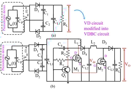
Figure 36.
Existing and proposed circuits: (a) voltage doubler; (b) voltage-doubled boost converter (VDBC) [100].
The main advantage of this topology is the minimized number of diodes which reduces the forward voltage loses. This schematic has six modes of operation. The detailed principle of operation could be found in [100]. The authors suggest the use of this circuit for low-voltage applications with an output voltage of 1–3 V. In those conditions, they were capable of converting 12.321 μW, which is much more in comparison with a test condition in which 11.7 V voltage was required. These circuits were mostly tested with low AC frequencies in the range of 5–20 Hz.
Another topology which represents a voltage doubler coupled with a boost converter was presented by the same author, A. Haseeb et al. [101]. In this design, a reduced number of switching elements (transistors) was used. The proposed topology is shown in Figure 37.
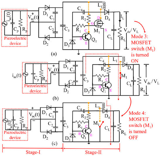
Figure 37.
The proposed topology of voltage doubler and boost converter: (a) Circuit diagram, (b) when the MOSFET switch (M1) is ON, (c) when the MOSFET switch (M1) is OFF [101].
The presented circuit has four modes of operation, which are described in [101]. In this work, the authors succeed in extracting 3.61 mW at an input frequency of 50 Hz and 0.396 mW at an input frequency of 1 Hz, which is better compared to their previous work.
The fourth selected work [102] was conducted by M. Kamran et al. They proposed a topology called full-bridge joule thief (FBRJT). In this topology, the authors used a full-bridge rectifier with a buck/boost converter. The proposed schematic is presented in Figure 38.
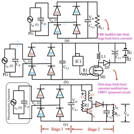
Figure 38.
The evolution of FBRJT topology: (a) Full-bridge rectifier, (b) Dual-stage buck-boost converter, (c) Proposed electronic circuit [102].
The schematic consists of two stages, a classical full-bridge rectifier and a buck/boost converter, and conducts six modes of operation, as described in [102]. The authors claim that the simplicity of this schematic, e.g., the use of coil coupled feedback instead of logic control, reduces the self-consumption power and improves the efficiency of the device [95]. The main advantage of this schematic is a particular optimization for low AC frequencies which are most likely related to normal human movements. The authors show a power of 3.41 mW delivered to the load with an efficiency of 71.5%.
The same author proposes another topology called voltage-doubler joule thief (VDJT) [103]. This concept is based on FBRJT topology but instead of a full-bridge rectifier a voltage doubler is used. The proposed schematic is shown in Figure 39.

Figure 39.
The evolution of VDJT topology [103].
The main difference between the two concepts (Figure 38 and Figure 39) is in Stage 1—the rectifier circuit. With this topology, the authors achieved an even higher output energy of 5.5 mW and a slightly higher efficiency of 72.3% in comparison to the FBRJT topology. They also report the need for investigation of the controlling methodology for the boost stage of the converter.
The sixth selected work [94] was conducted by L. Costanzo et al. and presents a device called the Energy Harvester Power Optimizer (EHPO). The schematic of this concept is presented in Figure 40.
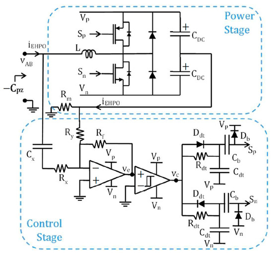
Figure 40.
The schematic of Energy Harvester Power Optimizer (EHPO) [94].
The EPHO topology consists of an AC-DC boost converter and a control loop. The control loop represents a kind of voltage comparator, while the design is described in detail in [94]. The theory of operation is based on controlled current draining from the piezoelectric generator and emulating a “negative” capacitance which increases the provided power. The authors also show a real-word example of this device which is capable of delivering 2.81 mW of power under sinusoidal conditions and 1.19 mW under non-sinusoidal conditions.
The last presented circuit was developed by Ben Ammar et al. [85] (Figure 41). This so-called interface circuit represents an energy harvesting device especially designed for footstep applications. The circuit consists of four main blocks: a piezoelectric energy harvester (PEH) and low-pass filter, a peak voltage detector and triggering circuit, a modified resonant (P-SSHI) circuit, and a GCC-based AC/DC rectifier.
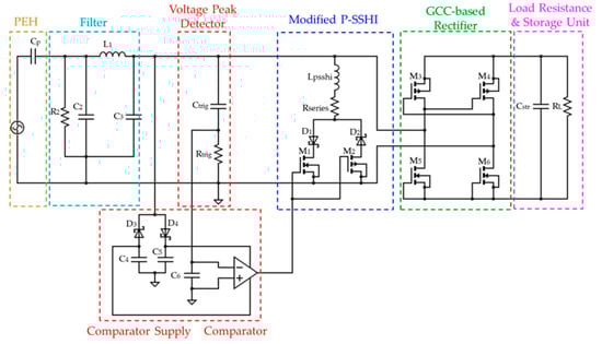
Figure 41.
Proposed energy harvesting circuit design for footstep applications [85].
A detailed description of each block and the principle of operation can be found in [96].
The practical realization of this device is capacitor charging. In the test setup, capacities of 1 mF and 10 µF were used. The authors reported a maximum energy efficiency of 83.33% when the delivered power was 3.6 mW.
In the Table 3, a comparative representation of the investigated devices [85,94,99,100,101,102,103] is presented. The most important parameters such as the output power reached and/or the efficiency for each device are presented. Also, the table describes the topology of the circuit as well as the main highlights for each approach.
Table 3.
Comparison of the described recent approaches for energy harvesting devices.
7. Concluding Remarks
This paper’s study objects are the approaches and techniques for designing power management systems intended for converting electrical energy from energy harvesters. As sources of electrical energy, the capabilities of piezoelectric elements are considered, in which the mechanical energy of vibrations is converted into electrical voltage and current. A typical Si-based cantilever piezoelectric element can generate electrical power in the range of 800 µW to 10–15 W, depending on factors such as the amplitude (1 g–10 kg) and frequency (10 Hz–200 kHz) of the applied mechanical vibrations, the size and geometry of the piezoelectric material (thickness of 0.8 µm–800 µm, linear dimensions of 10 mm–5 cm), and the specific piezoelectric coefficient of the material used (50–500 pC/N). They can also produce current outputs ranging from 100 nA to 100 µA, making them valuable components for applications requiring energy harvesting from ambient vibrations. When using piezoelectric elements as sources of electrical energy, an AC voltage with a non-sinusoidal waveform is obtained. The voltage has an approximately rectangular form, and more often it has an impulse character, i.e., short, intermittent pulses. Also, due to the spontaneous nature of mechanical vibrations, the amplitude of the produced AC voltage varies in a wide range and for a single element can have values of up to several volts and, in some cases, even 10 V or higher. If the produced electrical energy is used to supply a mixed-signal processing circuit or a microcontroller, the continuity of operation is necessary (i.e., constant value of the supply voltage during the operation), and an increase in the clock frequency results in an increase in the current consumption. All these conditions require a “short path” from the source of the electrical energy to the energy storage elements and also to the load, which in most cases is a supercapacitor, used as electrical energy storage elements. In this case, in the discharge mode of the electric energy storage element, the output current can reach values greater than 1 mA. To satisfy these conditions, there is a wide variety of low-power management systems, which in some cases are only a voltage rectifier or electronic AC/DC converter, employing a microcontroller as a switching circuit. At the same time, the quiescent current for the switching circuit does not exceed 1 μA at a relatively wide range of input voltage (from 1–2 V up to 20 V).
In this paper, the authors analyze the basic stage and functional blocks of an energy harvesting system from the signal source, through the electronic converter to the electrical energy storage elements. The structure of suitable piezoelectric elements for harvesting electrical energy is analyzed; then, a review of various types of low-power electronic circuits is performed, defining their advantages and disadvantages, and finally, the structure and operation principles of parallel-plate capacitors and thin-film supercapacitors suitable for wearable devices are discussed. Furthermore, the focus of the authors’ attention is on the various types of electronic circuits that can work with AC voltage obtained from piezoelectric elements and provide charging of a large-capacity electrolytic capacitor or supercapacitor. Since more and more electronic systems are implemented as laboratory monolithic integrated circuits, a comparative analysis was performed for them, indicating the most frequently used structural blocks with a definition of their basic electrical parameters and functional advantages. For all the circuits, the energy efficiency coefficient is greater than 60%, and for some of them, a value greater than 85% is achieved. For most of them, the output voltage is below 5 V when the input voltage changes to about 10 V. Also, a review of electronic systems using commercially available integrated circuits of micro-power management systems is carried out, and their structures and achieved functionalities are analyzed, including the possibility of wireless data transmission. For this class of integrated circuits, the typical value of the energy efficiency coefficient of most of them is greater than 60% but at values of the input voltage higher than 3 V and input current greater than 100 μA. However, as an advantage, it can be stated that most of them allow for several fixed values of the output voltage (up to 3.3 V) to be obtained at an output current of up to about 100 mA.
Based on the performed comparative analyses and the defined characteristics, the future work of the authors is aimed at synthesizing low-power piezoelectric energy harvesting circuits for wearable battery-free power supply devices, which are implemented on flexible printed circuit boards.
Author Contributions
Conceptualization, I.P., N.T., N.K. and M.A.; Investigation, I.P., N.K. and M.A.; Methodology, I.P.; Validation, I.P. and N.T.; Resources, I.P., N.K. and M.A.; Writing—Original Draft Preparation, I.P., N.T. and N.K.; Writing—Review and Editing, I.P., N.T., N.K. and M.A. All authors have read and agreed to the published version of the manuscript.
Funding
This study is financed by the European Union NextGenerationEU, through the National Recovery and Resilience Plan of the Republic of Bulgaria, project № BG-RRP-2.004-0005 “Improving research capacity and quality for international recognition and sustainability of the TU-Sofia”.
Data Availability Statement
Not applicable.
Acknowledgments
The authors wish to thank H.M. Antchev and D.D. Doychev for their helpful comments and suggestions.
Conflicts of Interest
The authors declare no conflicts of interest.
References
- Todaro, M.T.; Guido, F.; Algieri, L.; Mastronardi, V.M.; Desmaële, D.; Epifani, G.; De Vittorio, M. Biocompatible, Flexible, and Compliant Energy Harvesters Based on Piezoelectric Thin Films. IEEE Trans. Nanotechnol. 2018, 17, 220–230. [Google Scholar] [CrossRef]
- Amin, N.; Islam, S.K. Energy Harvesting in Implantable and Wearable Medical Devices for Enduring Precision Healthcare. Energies 2022, 15, 7495. [Google Scholar] [CrossRef]
- Fu, H.; Jiang, J.; Hu, S.; Rao, J.; Theodossiades, S. A multi-stable ultra-low frequency energy harvester using a nonlinear pendulum and piezoelectric transduction for self-powered sensing. Mech. Syst. Signal Process. 2023, 189, 110034. [Google Scholar] [CrossRef]
- Elfrink, R.; Matova, S.; de Nooijer, C.; Jambunathan, M.; Goedbloed, M.; van de Molengraft, J.; Pop, V.; Vullers, R.J.M.; Renaud, M.; van Schaijk, R. Shock induced energy harvesting with a MEMS harvester for automotive applications. In Proceedings of the 2011 International Electron Devices Meeting, Washington, DC, USA, 5–7 December 2011; pp. 29.5.1–29.5.4. [Google Scholar] [CrossRef]
- Shimanouchi, T.; Toyoda, O.; Nakazawa, F. A wireless motor-condition, precise analysis system using a highly efficient vibration-energy harvester. In Proceedings of the 11th IEEE International Conference on Industrial Informatics (INDIN), Bochum, Germany, 29–31 July 2013. [Google Scholar] [CrossRef]
- Rosa, R.L.; Costanza, M.; Livreri, P. Advanced Techniques for Powering Wireless Sensor Nodes through Energy Harvesting and Wireless Power Transfer. In Proceedings of the 2020 AEIT International Conference of Electrical and Electronic Technologies for Automotive (AEIT AUTOMOTIVE), Turin, Italy, 18–20 November 2020. [Google Scholar] [CrossRef]
- Romani, A.; Filippi, M.; Tartagni, M. Micropower Design of a Fully Autonomous Energy Harvesting Circuit for Arrays of Piezoelectric Transducers. IEEE Trans. Power Electron. 2014, 29, 729–739. [Google Scholar] [CrossRef]
- Aktakka, E.E.; Najafi, K. A Micro Inertial Energy Harvesting Platform with Self-Supplied Power Management Circuit for Autonomous Wireless Sensor Nodes. IEEE J. Solid-State Circuits 2014, 49, 2017–2029. [Google Scholar] [CrossRef]
- Liu, W.; Wang, Z.; Qu, S.; Luo, R. Vibration energy harvesting and management for wireless sensor networks in bridge structural monitoring. In Proceedings of the 2015 IEEE SENSORS, Busan, Republic of Korea, 1–4 November 2015. [Google Scholar] [CrossRef]
- Han, Y.; Feng, Y.; Yu, Z.; Lou, W.; Liu, H. A Study on Piezoelectric Energy-Harvesting Wireless Sensor Networks Deployed in a Weak Vibration Environment. IEEE Sens. J. 2017, 17, 6770–6777. [Google Scholar] [CrossRef]
- Huet, F.; Boitier, V.; Seguier, L. Tunable Piezoelectric Vibration Energy Harvester with Supercapacitors for WSN in an Industrial Environment. IEEE Sens. J. 2022, 22, 15373–15384. [Google Scholar] [CrossRef]
- Caliò, R.; Rongala, U.B.; Camboni, D.; Milazzo, M.; Stefanini, C.; De Petris, G.; Oddo, C.M. Piezoelectric Energy Harvesting Solutions. Sensors 2014, 14, 4755–4790. [Google Scholar] [CrossRef] [PubMed]
- Li, H.; Tian, C.; Deng, D. Energy harvesting from low frequency applications using piezoelectric materials. Appl. Phys. Rev. 2014, 1, 041301. [Google Scholar] [CrossRef]
- Priya, S.; Song, H.-C.; Zhou, Y.; Varghese, R.; Chopra, A.; Kim, S.-G.; Kanno, I.; Wu, L.; Ha, D.S.; Ryu, J.; et al. A Review on Piezoelectric Energy Harvesting: Materials, Methods, and Circuits. Energy Harvest. Syst. Actuators 2017, 4, 3–39. [Google Scholar] [CrossRef]
- Covaci, C.; Gontean, A. Piezoelectric Energy Harvesting Solutions: A Review. Sensors 2020, 20, 3512. [Google Scholar] [CrossRef] [PubMed]
- Tamburrano, P.; Sciatti, F.; Plummer, A.R.; Distaso, E.; De Palma, P.; Amirante, R. A Review of Novel Architectures of Servovalves Driven by Piezoelectric Actuators. Energies 2021, 14, 4858. [Google Scholar] [CrossRef]
- Brusa, E.; Carrera, A.; Delprete, C. A Review of Piezoelectric Energy Harvesting: Materials, Design, and Readout Circuits. Actuators 2023, 12, 457. [Google Scholar] [CrossRef]
- Mishra, P.; Singh, G. Energy Management Systems in Sustainable Smart Cities Based on the Internet of Energy: A Technical Review. Energies 2023, 16, 6903. [Google Scholar] [CrossRef]
- Hezekiah, J.D.K.; Ramya, K.C.; Radhakrishnan, S.B.K.; Kumarasamy, V.M.; Devendran, M.; Ramalingam, A.; Maheswar, R. Review of Next-Generation Wireless Devices with Self-Energy Harvesting for Sustainability Improvement. Energies 2023, 16, 5174. [Google Scholar] [CrossRef]
- Dziadak, B.; Makowski, Ł.; Kucharek, M.; Jóśko, A. Energy Harvesting for Wearable Sensors and Body Area Network Nodes. Energies 2023, 16, 1681. [Google Scholar] [CrossRef]
- Katche, M.L.; Makokha, A.B.; Zachary, S.O.; Adaramola, M.S. A Comprehensive Review of Maximum Power Point Tracking (MPPT) Techniques Used in Solar PV Systems. Energies 2023, 16, 2206. [Google Scholar] [CrossRef]
- Nwalike, E.D.; Ibrahim, K.A.; Crawley, F.; Qin, Q.; Luk, P.; Luo, Z. Harnessing Energy for Wearables: A Review of Radio Frequency Energy Harvesting Technologies. Energies 2023, 16, 5711. [Google Scholar] [CrossRef]
- Haider, S.T.; Shah, M.A.; Lee, D.-G.; Hur, S. A Review of the Recent Applications of Aluminum Nitride-Based Piezoelectric Devices. IEEE Access 2023, 11, 58779–58795. [Google Scholar] [CrossRef]
- Ottman, G.K.; Hofmann, H.F.; Bhatt, A.C.; Lesieutre, G.A. Adaptive piezoelectric energy harvesting circuit for wireless remote power supply. IEEE Trans. Power Electron. 2002, 17, 669–676. [Google Scholar] [CrossRef]
- Tabesh, A.; Fréchette, L. An improved small-deflection electromechanical model for piezoelectric bending beam actuators and energy harvesters. J. Micromechanics Microengineering 2008, 18, 104009. [Google Scholar] [CrossRef]
- Sezer, N.; Koç, M. A comprehensive review on the state-of-the-art of piezoelectric energy harvesting. Nano Energy 2021, 80, 105567. [Google Scholar] [CrossRef]
- Wei, C.; Jing, X. A comprehensive review on vibration energy harvesting: Modelling and realization. Renew. Sustain. Energy Rev. 2017, 74, 1–18. [Google Scholar] [CrossRef]
- Liang, J.; Liao, W.-H. Impedance matching for improving piezoelectric energy harvesting systems. In Proceedings of the SPIE—The International Society for Optical Engineering, San Diego, CA, USA, 6–10 March 2010. [Google Scholar] [CrossRef]
- ABT-441-RC; Piezo Element, 27 mm, 4200 Hz, Leaded—Datasheet. MULTICOMP PRO: Chicago, IL, USA. 2020. Available online: https://uk.farnell.com/multicomp/abt-441-rc/transducer-piezo-4200hz-30v/dp/1675548 (accessed on 11 September 2023).
- ABT-448-90-RC; Piezo Element, 35 mm, 2900 Hz, Leaded—Datasheet. MULTICOMP PRO: Chicago, IL, USA. 2019. Available online: https://uk.farnell.com/multicomp/abt-448-90-rc/piezo-element-35mm-2-900hz-leaded/dp/1675549?ost=abt-448-90-rc (accessed on 11 September 2023).
- PPA PRODUCTS Datasheet & User Manual; Midé Technology: Medford, MA, USA. 2020. Available online: https://cdn2.hubspot.net/hubfs/3841176/Data-Sheets/ppa-piezo-product-datasheet.pdf (accessed on 27 May 2024).
- Wakshume, D.G.; Płaczek, M.Ł. Optimizing Piezoelectric Energy Harvesting from Mechanical Vibration for Electrical Efficiency: A Comprehensive Review. Electronics 2024, 13, 987. [Google Scholar] [CrossRef]
- He, M.; He, M.; Zhang, X.; Xia, L. Topology Optimization of Piezoelectric Energy Harvesters for Enhanced Open-Circuit Voltage Subjected to Harmonic Excitations. Materials 2022, 15, 4423. [Google Scholar] [CrossRef]
- Safaei, M.; Sodanoand, H.A.; Anton, S.R. A review of energy harvesting using piezoelectric materials: State-of-the-art a decade later (2008–2018). Smart Mater. Struct. 2019, 28, 113001. [Google Scholar] [CrossRef]
- Ichige, R.; Kuriyama, N.; Umino, Y.; Tsukamoto, T.; Suzuki, T. Size optimization of metamaterial structure for elastic layer of a piezoelectric vibration energy harvester. Sens. Actuators A Phys 2021, 318, 112488. [Google Scholar] [CrossRef]
- Elvira-Hernández, E.A.; Woo-García, R.M.; López-Huerta, F.; Vázquez-Leal, H.; Herrera-May, A.L. Design of a MEMS-Based Piezoelectric Vibration Energy Harvesting Device for Automotive Applications. Comput. Sist. 2019, 23, 71–79. [Google Scholar] [CrossRef]
- Stamatellou, A.M. PZT and PVDF piezoelectric transducers’ design implications on their efficiency and energy harvesting potential. Energy Harvest. Syst. 2023, 10, 157–167. [Google Scholar] [CrossRef]
- Feng, H.; Bu, L.; Li, Z.; Xu, S.; Hu, B.; Xu, M.; Jiang, S.; Wang, X. Multimodal MEMS vibration energy harvester with cascaded flexible and silicon beams for ultralow frequency response. Microsyst. Nanoeng. 2023, 9, 33. [Google Scholar] [CrossRef]
- Zhang, L.; Gui, J.; Wu, Z.; Li, R.; Wang, Y.; Gong, Z.; Zhao, X.; Sun, C.; Guo, S. Enhanced performance of piezoelectric nanogenerator based on aligned nanofibers and three-dimensional interdigital electrodes. Nano Energy 2019, 65, 103924. [Google Scholar] [CrossRef]
- Huang, M.; Hou, C.; Li, Y.; Liu, H.; Wang, F.; Chen, T.; Yang, Z.; Tang, G.; Sun, L. A Low-Frequency MEMS Piezoelectric Energy Harvesting System Based on Frequency Up-Conversion Mechanism. Micromachines 2019, 10, 639. [Google Scholar] [CrossRef] [PubMed]
- Hossain, M.I.; Zahid, M.S.; Chowdhury, M.A.; Hossain MM, M.; Hossain, N. MEMS-based energy harvesting devices for low-power applications—A review. Results Eng. 2023, 19, 101264. [Google Scholar] [CrossRef]
- Zhang, M.; Zhang, A.M.; Chen, Y.; Xie, J.; Xin, Z.F.; Chen, Y.J.; Kan, Y.H.; Li, S.L.; Lan, Y.Q.; Zhang, Q. Polyoxovanadate-polymer hybrid electrolyte in solid state batteries. Energy Storage Mater. 2020, 29, 172–181. [Google Scholar] [CrossRef]
- Dutta, S.; Pandey, A. Overview of residual stress in MEMS structures: Its origin, measurement, and control. J. Mater. Sci. Mater. Electron. 2021, 32, 6705–6741. [Google Scholar] [CrossRef]
- Aleksandrova, M. Polymeric seed layer as a simple approach for nanostructuring of Ga-doped ZnO films for flexible piezoelectric energy harvesting. Microelectron. Eng. 2020, 233, 111434. [Google Scholar] [CrossRef]
- Stefanov, N. Special rectifiers, and Power rectifiers. In Power Supply Devices; Tehnika: Sofia, Bulgaria, 2002; Chapters 2 and 4; pp. 43–68, 84–96. ISBN 9789540305646. (In Bulgarian) [Google Scholar]
- Tietze, V.; Schenk, C. Power Supplies In Electronic circuits, 2nd ed.; Springer: New York, NY, USA, 2008; Chapter 16; pp. 885–928. [Google Scholar] [CrossRef]
- Gates Energy Products, Typical Application for Sealed Nickel-cadmium Batteries. In Rechargeable Batteries Application Handbook; Butterworth-Heinemann: Boston, MA, USA; London, UK, 1992; pp. 35–152.
- Aleksandrova, M.; Pandiev, I. Application of Thin Film Ultralow-Power Lead-Free Perovskite Solar Energy Harvesters in Power Management Systems. In Proceedings of the 28 International Conference Mixed Design of Integrated Circuits and Systems, MIXDES 2021, Łódź, Poland, 24–26 June 2021. [Google Scholar] [CrossRef]
- Asthana, P.; Khanna, G. Power amplification interface circuit for broadband piezoelectric energy harvester. Microelectron. J. 2020, 98, 104734. [Google Scholar] [CrossRef]
- Dicken, J.; Mitcheson, P.D.; Stoianov, I.; Yeatman, E.M. Power-Extraction Circuits for Piezoelectric Energy Harvesters in Miniature and Low-Power Applications. IEEE Trans. Power Electron. 2012, 27, 4514–4529. [Google Scholar] [CrossRef]
- Szarka, G.D.; Stark, B.H.; Burrow, S.G. Review of Power Conditioning for Kinetic Energy Harvesting Systems. IEEE Trans. Power Electron. 2012, 27, 803–815. [Google Scholar] [CrossRef]
- Faghihi, S.; Moallem, M. Analysis and design of a low power electronics circuit for energy harvesting applications. In Proceedings of the 2012 IEEE International Symposium on Industrial Electronics, Hangzhou, China, 28–31 May 2012. [Google Scholar] [CrossRef]
- Du, S.; Seshia, A.A. An Inductorless Bias-Flip Rectifier for Piezoelectric Energy Harvesting. IEEE J. Solid-State Circuits 2017, 52, 2746–2757. [Google Scholar] [CrossRef]
- Richard, C.; Guyomar, D.; Audigier, D.; Ching, G. Semi Passive Damping using Continuous Switching of a Piezoelectric Device. In Proceedings of the SPIE Smart Structures and Materials Conference, Passive Damping and Isolation, San Diego, CA, USA, 1–2 March 1999. [Google Scholar]
- Guyomar, D.; Richard, C.; Lefeuvre, E.; Petit, L. Piezoelectric Non-linear Systems for Standalone Vibration Control and Energy Reclamation. In Proceedings of the AC’04, Hildesheim, Germany, 27–28 April 2004. [Google Scholar]
- Badel, A.; Guyomar, D.; Lefeuvre, E.; Richard, C. Efficiency enhancement of a piezoelectric energy harvesting device in pulsed operation by synchronous charge inversion. J. Intell. Mater. Syst. Struct. 2005, 16, 889–901. [Google Scholar] [CrossRef]
- Dicken, J.; Mitcheson, P.D.; Stoianov, I.; Yeatman, E.M. Increased power output from piezoelectric energy harvesters by pre-biasing. In Proceedings of the 9th International Workshop on Micro and Nanotechnology for Power Generation and Energy Conversion Applications (PowerMEMS), Washington, DC, USA, 1–4 December 2009; pp. 75–78. [Google Scholar]
- Oh, T.; Islam, S.K.; To, G.; Mahfouz, M. Powering wearable sensors with a low-power CMOS piezoelectric energy harvesting circuit. In Proceedings of the 2017 IEEE International Symposium on Medical Measurements and Applications (MeMeA), Rochester, MN, USA, 7–10 May 2017. [Google Scholar] [CrossRef]
- Chew, Z.J.; Zhu, M. Adaptive Self-Configurable Rectifier for Extended Operating Range of Piezoelectric Energy Harvesting. IEEE Trans. Ind. Electron. 2020, 67, 3267–3276. [Google Scholar] [CrossRef]
- Tabesh, A.; Frechette, L.G. A Low-Power Stand-Alone Adaptive Circuit for Harvesting Energy From a Piezoelectric Micropower Generator. IEEE Trans. Ind. Electron. 2010, 57, 840–849. [Google Scholar] [CrossRef]
- Pandiev, I.; Aleksandrova, M.; Kolev, G. Design and Implementation of Interface Circuits Intended for Printed Piezoelectric Micropower Harvesters on Flexible Substrates. IOP Conf. Ser. Mater. Sci. Eng. 2020, 876, 012007. [Google Scholar] [CrossRef]
- Brenes, A.; Morel, A.; Juillard, J.; Lefeuvre, E.; Badel, A. Maximum power point of piezoelectric energy harvesters: A review of optimality condition for electrical tuning. Smart Mater. Struct. 2020, 29, 033001. [Google Scholar] [CrossRef]
- Du, S.; Jia, Y.; Do, C.D.; Seshia, A.A. An Efficient SSHI Interface with Increased Input Range for Piezoelectric Energy Harvesting Under Variable Conditions. IEEE J. Solid-State Circuits 2016, 51, 2729–2742. [Google Scholar] [CrossRef]
- Liu, Z.; Zhao, C.; Hu, G.; Yang, Y. A multi-degree-of-freedom triboelectric energy harvester for dual-frequency vibration energy harvesting. Mech. Syst. Signal Process. 2023, 188, 1–20. [Google Scholar] [CrossRef]
- Lefeuvre, E.; Badel, A.; Richard, C.; Petit, L.; Guyomar, D. A comparison between several vibration-powered piezoelectric generators for standalone systems. Sens. Actuators A Phys. 2006, 126, 405–416. [Google Scholar] [CrossRef]
- Seifart, M. Stromversorgung. In Analoge Schaltungen, 6th ed.; Technik: Berlin, Germany, 2003; Chapter 22; pp. 591–639. [Google Scholar]
- Farhi, S.; Papazov, S. Introduction to Electromagnetism. In Theoretical Electric Engineering, 2nd ed.; Tehnika: Sofia, Bulgaria, 1987; Chapter 1; Part 1, pp. 5–46. (In Bulgarian) [Google Scholar]
- Polymer Aluminum Solid Electrolytic Capacitors MA Series—Datasheet; Fujicon Electric Company: Kowloon, Hong Kong. 2024. Available online: http://www.fujicon.com/pdf/products/MA.pdf (accessed on 24 May 2024).
- Polymer Aluminum Solid Electrolytic Capacitors FZ Series—Datasheet. Fujicon Electric Company. Hunghom Commercial Centre, Tower A, 39 Ma Tau Wai Road, Hung Hom, Kowloon, Hong Kong. 2024. Available online: http://www.fujicon.com/pdf/products/FZ.pdf (accessed on 24 May 2024).
- Surface-Mount Ceramic Multilayer Capacitors—Datasheet. YAGEO, 3F, 233–1, Baoqiao Rd. Xindian Dist., New Taipei City 23145 Taiwan. 2024. Available online: https://www.yageo.com/upload/media/product/products/datasheet/mlcc/UPY-AC_NP0X7RX7S_6.3V-to-2KV_20.pdf (accessed on 24 May 2024).
- Halper, M.S.; Ellenbogen, J.C. Supercapacitors: A Brief Overview; MITRE Nanosystems Group: McLean, VA, USA, 2006; Available online: http://www.mitre.org/sites/default/files/pdf/06_0667.pdf (accessed on 24 May 2024).
- Sherrard, C.G.; Rolin, T.D. Solid-State Ultracapacitor Polymer Composite; National Aeronautics and Space Administration, Marshall Space Flight Center: Huntsville, AL, USA, 2022. Available online: https://ntrs.nasa.gov/citations/20220018181 (accessed on 24 May 2024).
- Yoshida, A.; Imoto, K.; Yoneda, H.; Nishimo, A. An electric double-layer capacitor with high capacitance and low resistance. IEEE Trans. Compon. Hybrids Manuf. Technol. 1992, 15, 133–138. [Google Scholar] [CrossRef]
- Bonert, R.; Zubieta, L. Measurement techniques for the evaluation of double-layer power capacitors, IAS ’97. In Proceedings of the 1997 IEEE Industry Applications Conference Thirty-Second IAS Annual Meeting, New Orleans, LA, USA, 5–9 October 1997. [Google Scholar] [CrossRef]
- Zubieta, L.; Bonert, R. Characterization of double-layer capacitors (DLCs) for power electronics applications. In Proceedings of the 1998 IEEE Industry Applications Conference. Thirty-Third IAS Annual Meeting (Cat. No.98CH36242), St. Louis, MO, USA, 12–15 October1998. [Google Scholar] [CrossRef]
- Belhachemi, F.; Rael, S.; Davat, B. A physical based model of power electric double-layer supercapacitors. In Proceedings of the 2000 IEEE Industry Applications Conference. Thirty-Fifth IAS Annual Meeting and World Conference on Industrial Applications of Electrical Energy (Cat. No.00CH37129), Rome, Italy, 8–12 October 2000. [Google Scholar] [CrossRef]
- Naguib, M.; Mochalin, V.N.; Barsoum, M.W.; Gogotsi, Y. 25th anniversary article: MXenes: A new family of two-dimensional materials. Adv. Mater. 2014, 26, 992–1005. [Google Scholar] [CrossRef]
- Xu, S.; Liu, W.; Liu, X.; Kuang, X.; Wang, X. A MXene based all-solid-state microsupercapacitor with 3D interdigital electrode. In Proceedings of the 19th International Conference on Solid-State Sensors, Actuators and Microsystems (TRANSDUCERS), Kaohsiung, Taiwan, 18–22 June 2017. [Google Scholar] [CrossRef]
- Tuzluca, F.N.; Yesilbag, Y.O.; Shafiee, F.N.; Hamidon, M.N.; Ertugrul, M. Two Dimensional Ti3C2Tx MXene Electrode For Supercapacitor Application. In Proceedings of the 2019 IEEE Regional Symposium on Micro and Nanoelectronics (RSM), Pahang, Malaysia, 21–23 August 2019. [Google Scholar] [CrossRef]
- Panda, S.; Deshmukh, K.; Pasha, S.K.K.; Theerthagiri, J.; Manickam, S.; Choi, M.Y. MXene based emerging materials for supercapacitor applications: Recent advances, challenges, and future perspectives. Coord. Chem. Rev. 2022, 462, 214518. [Google Scholar] [CrossRef]
- Sanchez, D.A.; Leicht, J.; Jodka, E.; Fazel, E.; Manoli, Y. 21.2 A 4 µW-to-1 mW parallel-SSHI rectifier for piezoelectric energy harvesting of periodic and shock excitations with inductor sharing, cold start-up and up to 681% power extraction improvement. In Proceedings of the 2016 IEEE International Solid-State Circuits Conference (ISSCC), San Francisco, CA, USA, 31 January–4 February 2016. [Google Scholar] [CrossRef]
- Wu, L.; Do, X.-D.; Lee, S.-G.; Ha, D.S. A Self-Powered and Optimal SSHI Circuit Integrated with an Active Rectifier for Piezoelectric Energy Harvesting. IEEE Trans. Circuits Syst. I Regul. Pap. 2017, 64, 537–549. [Google Scholar] [CrossRef]
- Chamanian, S.; Çiftci, B.; Muhtaroğlu, A.; Külah, H. A Self-Powered and Area Efficient SSHI Rectifier for Piezoelectric Harvesters. IEEE Access 2021, 9, 117703–117713. [Google Scholar] [CrossRef]
- Çiftci, B.; Chamanian, S.; Koyuncuoğlu, A.; Muhtaroğlu, A.; Külah, H. A Low-Profile Autonomous Interface Circuit for Piezoelectric Micro-Power Generators. IEEE Trans. Circuits Syst. I Regul. Pap. 2021, 68, 1458–1471. [Google Scholar] [CrossRef]
- Ben Ammar, M.; Sahnoun, S.; Fakhfakh, A.; Viehweger, C.; Kanoun, O. Self-Powered Synchronized Switching Interface Circuit for Piezoelectric Footstep Energy Harvesting. Sensors 2023, 23, 1830. [Google Scholar] [CrossRef] [PubMed]
- Ramadass, Y.K.; Chandrakasan, A.P. An Efficient Piezoelectric Energy Harvesting Interface Circuit Using a Bias-Flip Rectifier and Shared Inductor. IEEE J. Solid-State Circuits 2010, 45, 189–204. [Google Scholar] [CrossRef]
- Li, S.; Roy, A.; Calhoun, B.H. A Piezoelectric Energy-Harvesting System with Parallel-SSHI Rectifier and Integrated MPPT Achieving 417% Energy-Extraction Improvement and 97% Tracking Efficiency. In Proceedings of the 2019 Symposium on VLSI Circuits, Kyoto, Japan, 9–14 June 2019. [Google Scholar] [CrossRef]
- Du, S.; Jia, Y.; Zhao, C.; Amaratunga GA, J.; Seshia, A.A. A Fully Integrated Split-Electrode SSHC Rectifier for Piezoelectric Energy Harvesting. IEEE J. Solid-State Circuits 2019, 54, 1733–1743. [Google Scholar] [CrossRef]
- Peng, Y.; Choo, K.D.; Oh, S.; Lee, I.; Jang, T.; Kim, Y.; Lim, J.; Blaauw, D.; Sylvester, D. An Efficient Piezoelectric Energy Harvesting Interface Circuit Using a Sense-and-Set Rectifier. IEEE J. Solid-State Circuits 2019, 54, 3348–3361. [Google Scholar] [CrossRef]
- Khan, M.B.; Saif, H.; Lee, Y. A Piezoelectric Energy Harvesting Interface for Irregular High Voltage Input with Partial Electric Charge Extraction with 3.9× Extraction Improvement. In Proceedings of the 2019 IEEE Asian Solid-State Circuits Conference (A-SSCC), Macau, Macao, 4–6 November 2019. [Google Scholar] [CrossRef]
- Kwon, D.; Rincón-Mora, G.A. A Single-Inductor 0.35 µm CMOS Energy-Investing Piezoelectric Harvester. IEEE J. Solid-State Circuits 2014, 49, 2277–2291. [Google Scholar] [CrossRef]
- Chamanian, S.; Muhtaroğlu, A.; Külah, H. A Self-Adapting Synchronized-Switch Interface Circuit for Piezoelectric Energy Harvesters. IEEE Trans. Power Electron. 2020, 35, 901–912. [Google Scholar] [CrossRef]
- Du, S.; Amaratunga GA, J.; Seshia, A.A. A Cold-Startup SSHI Rectifier for Piezoelectric Energy Harvesters with Increased Open-Circuit Voltage. IEEE Trans. Power Electron. 2019, 34, 263–274. [Google Scholar] [CrossRef]
- Costanzo, L.; Lo Schiavo, A.; Vitelli, M. A Self-Supplied Power Optimizer for Piezoelectric Energy Harvesters Operating under Non-Sinusoidal Vibrations. Energies 2023, 16, 4368. [Google Scholar] [CrossRef]
- Hehn, T.; Hagedorn, F.; Maurath, D.; Marinkovic, D.; Kuehne, I.; Frey, A.; Manoli, Y. A Fully Autonomous Integrated Interface Circuit for Piezoelectric Harvesters. IEEE J. Solid-State Circuits 2012, 47, 2185–2198. [Google Scholar] [CrossRef]
- LTC3588-1; Nanopower Energy Harvesting Power Supply—Datasheet. Analog Devices: Norwood, MA, USA. 2023. Available online: https://www.analog.com/en/products/ltc3588-1.html (accessed on 16 October 2023).
- ADP5092; Ultralow Power Energy Harvester PMU with MPPT and Charge Management—Datasheet. Analog Devices: Norwood, MA, USA. 2023. Available online: https://www.analog.com/en/products/adp5092.html (accessed on 16 October 2023).
- MAX20361; Small, Single-/Multi-Cell Solar Harvester with MPPT and Harvest Counter—Datasheet. Analog Devices: Norwood, MA, USA. 2023. Available online: https://www.analog.com/en/products/max20361.html (accessed on 16 October 2023).
- Edla, M.; Lim, Y.Y.; Mikio, D.; Padilla, R.V. Non-Linear Switching Circuit for Active Voltage Rectification and Ripples Reduction of Piezoelectric Energy Harvesters. Energies 2022, 15, 709. [Google Scholar] [CrossRef]
- Haseeb, A.; Edla, M.; Ucgul, M.; Santoso, F.; Deguchi, M. A Voltage Doubler Boost Converter Circuit for Piezoelectric Energy Harvesting Systems. Energies 2023, 16, 1631. [Google Scholar] [CrossRef]
- Haseeb, A.; Edla, M.; Thabet, A.M.; Deguchi, M.; Kamran, M. A Self-Powered Dual-Stage Boost Converter Circuit for Piezoelectric Energy Harvesting Systems. Energies 2023, 16, 2490. [Google Scholar] [CrossRef]
- Kamran, M.; Edla, M.; Thabet, A.M.; Haseeb, A.; Mikio, D.; Bui, V. A Self-Powered FBRJT AC-DC Conversion Circuit for Piezoelectric Energy Harvesting Systems. Energies 2023, 16, 1734. [Google Scholar] [CrossRef]
- Kamran, M.; Edla, M.; Thabet, A.M.; Mikio, D.; Bui, V. A Self-Powered VDJT AC–DC Conversion Circuit for Piezoelectric Energy Harvesting Systems. Designs 2023, 7, 94. [Google Scholar] [CrossRef]
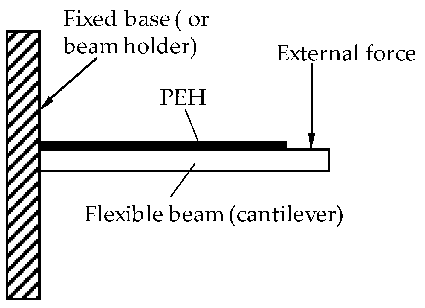
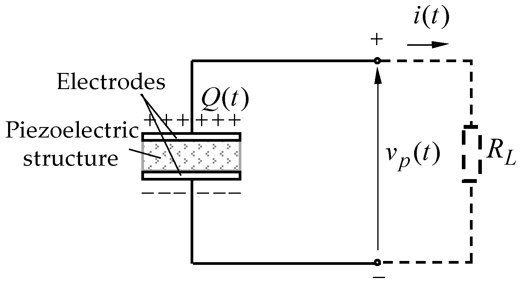

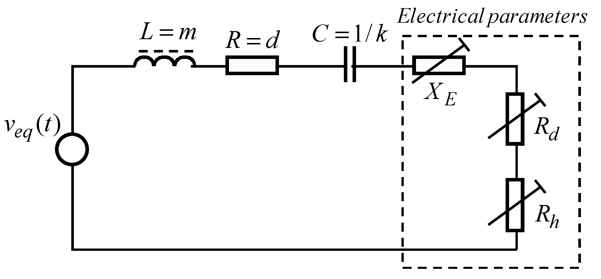
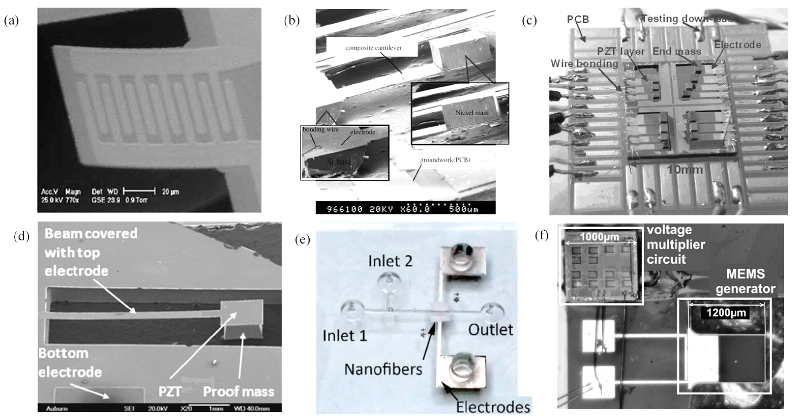
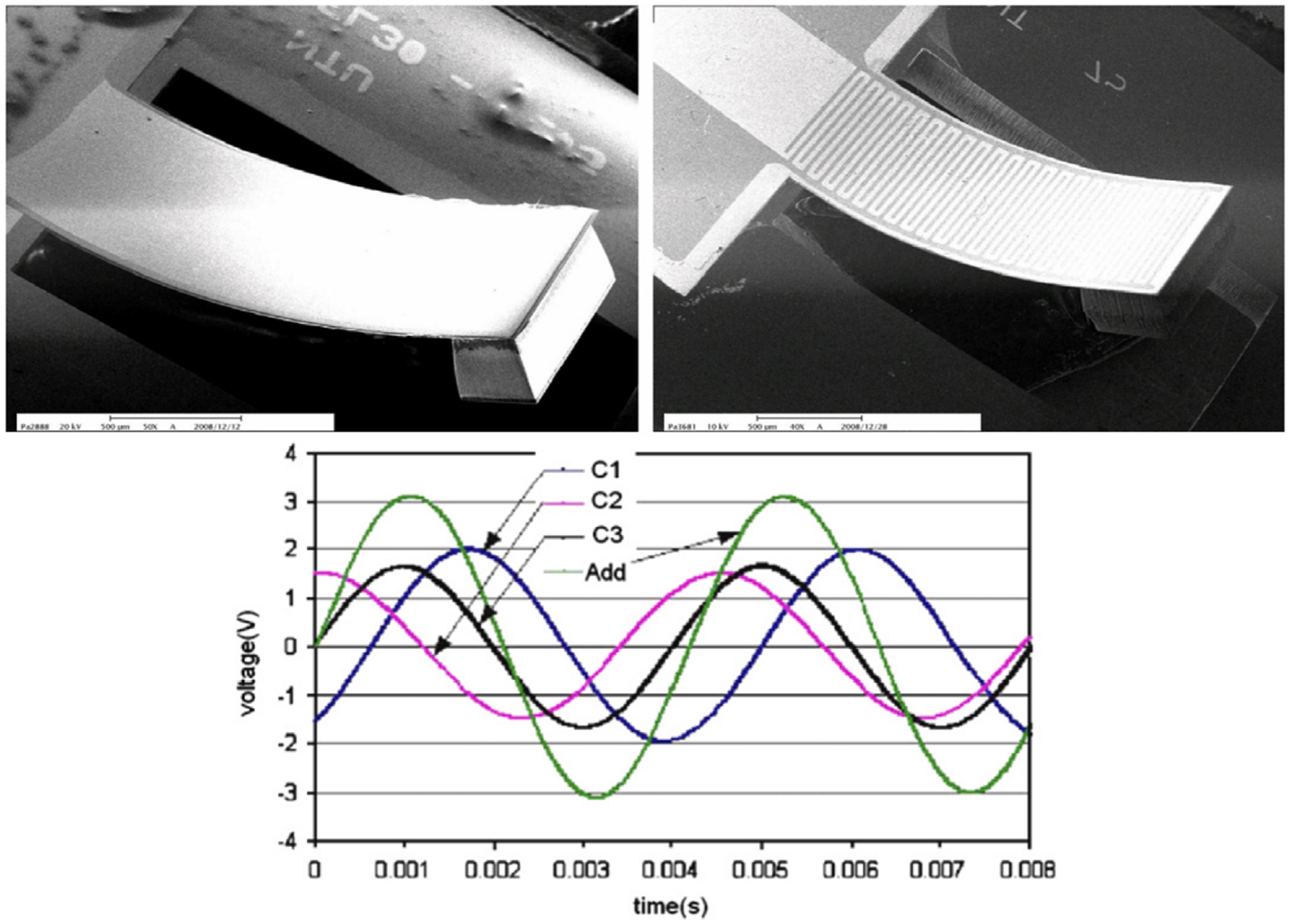
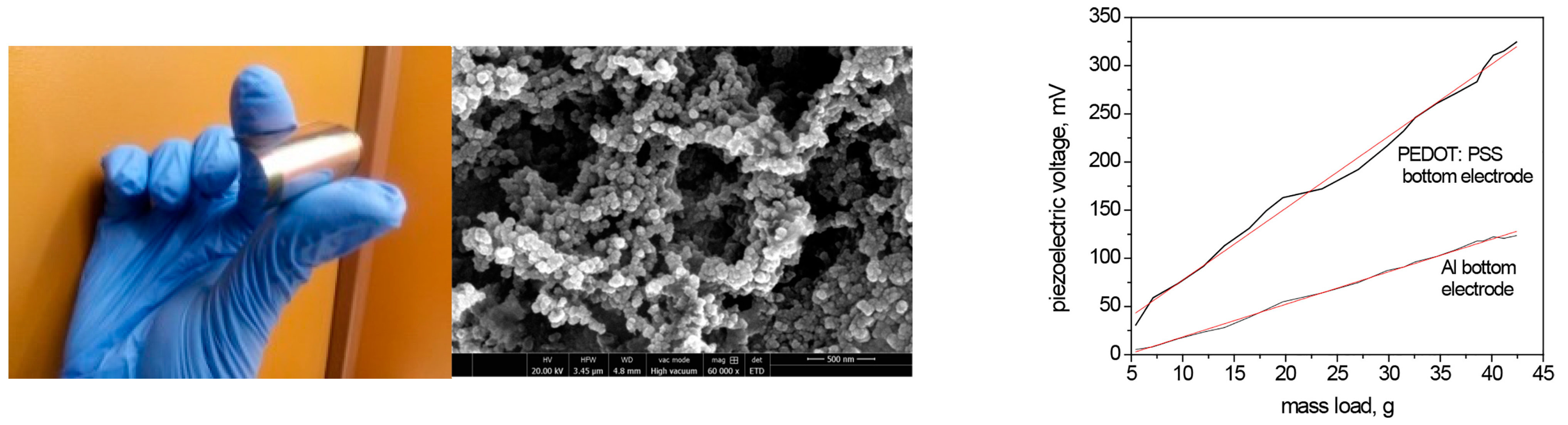
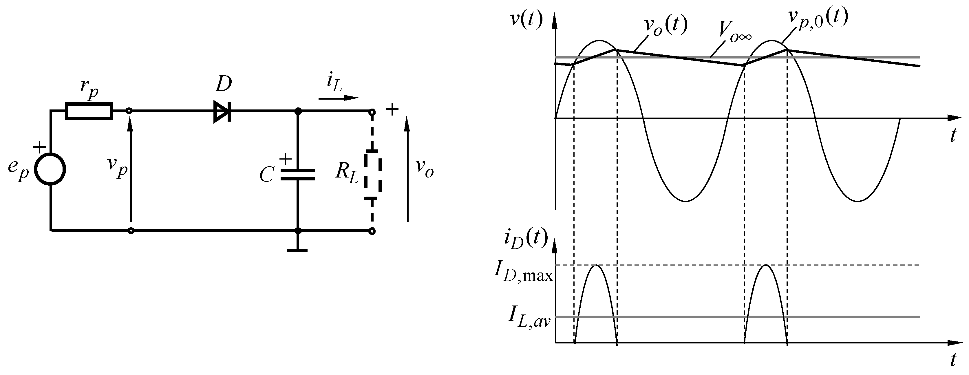

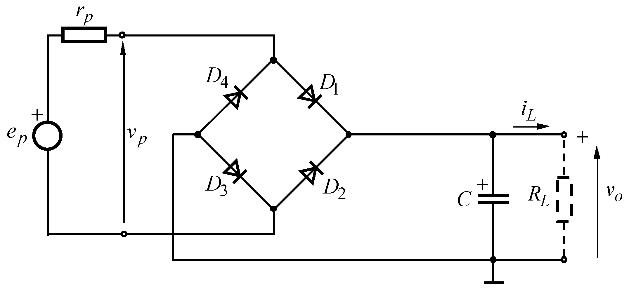
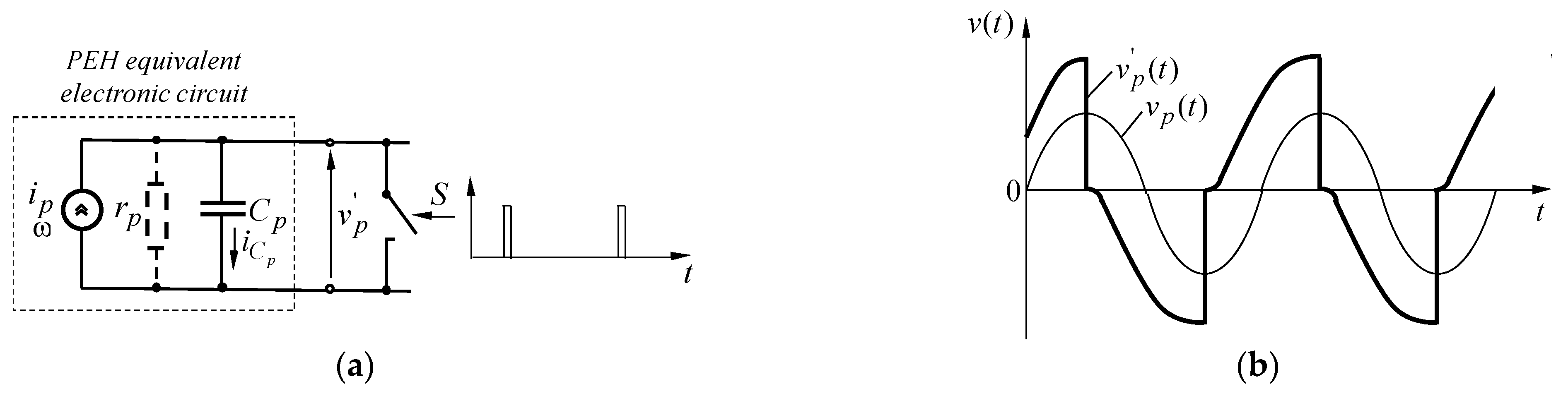

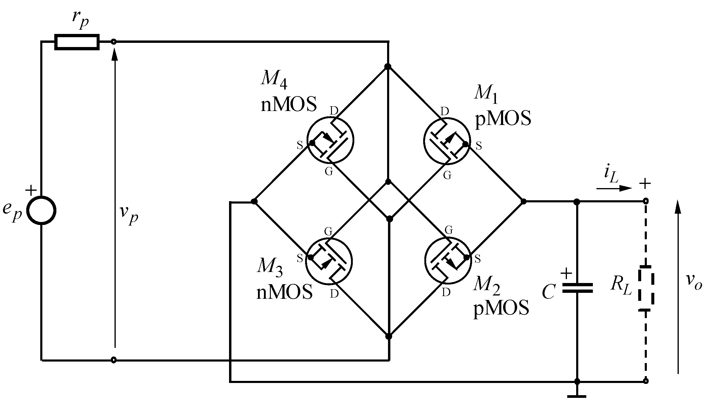

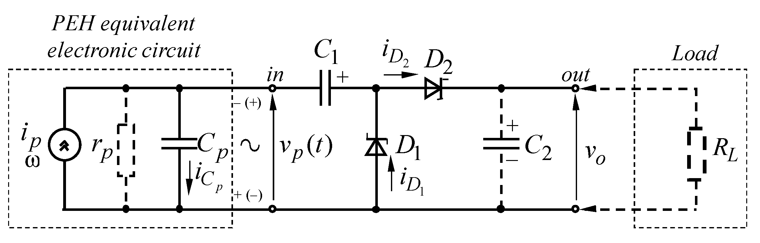
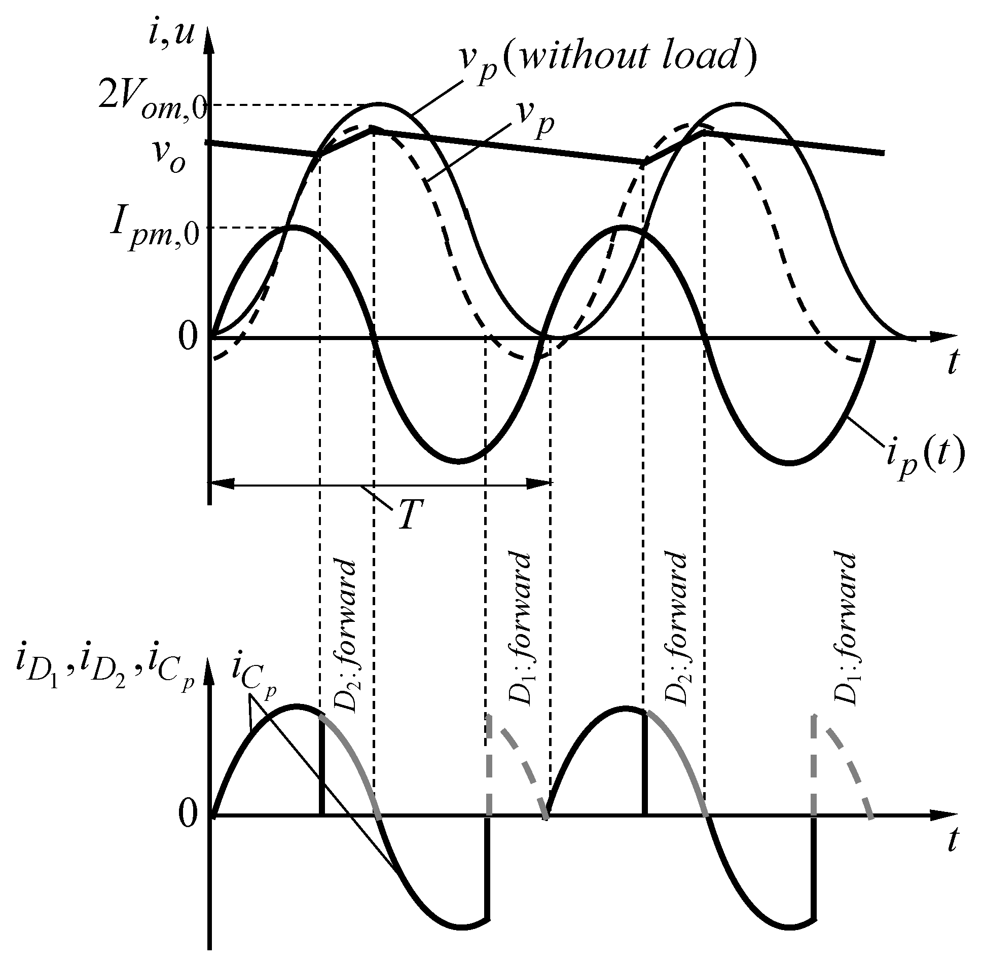

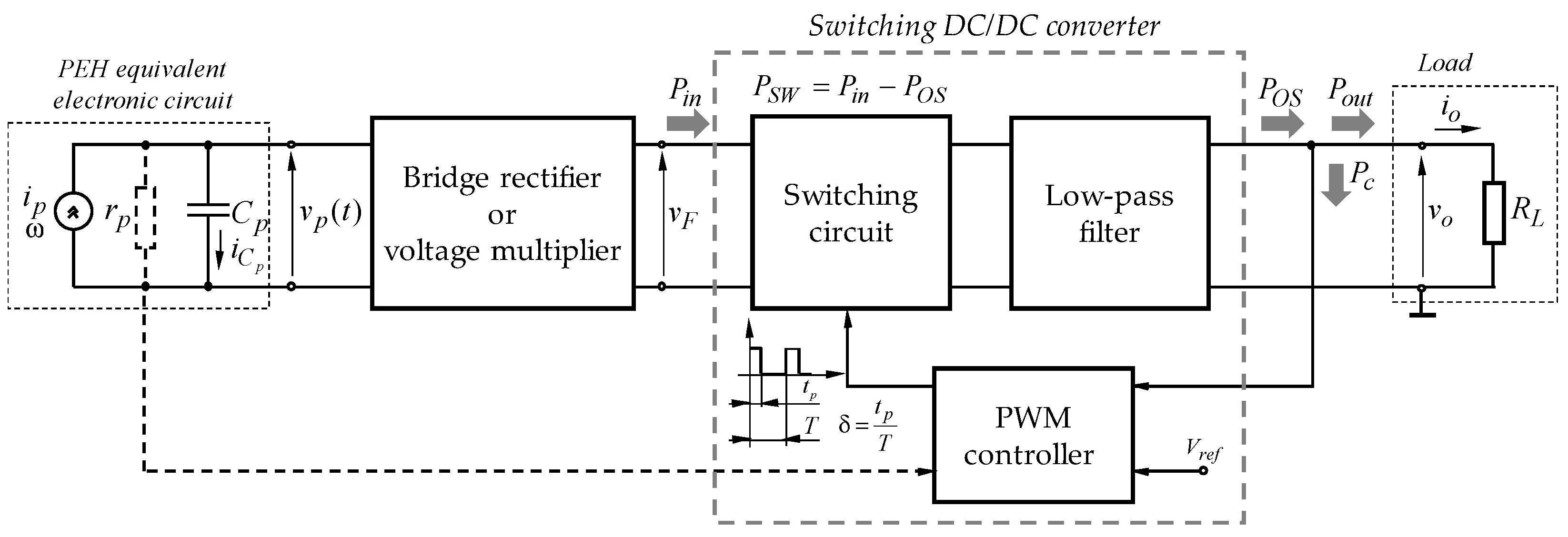
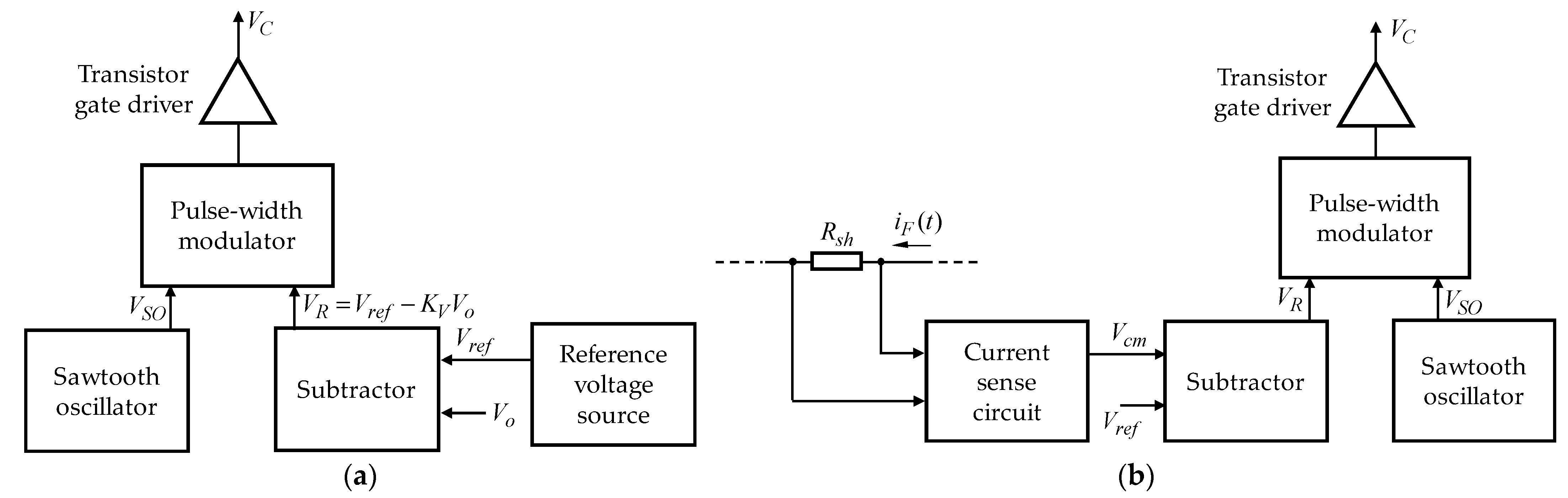
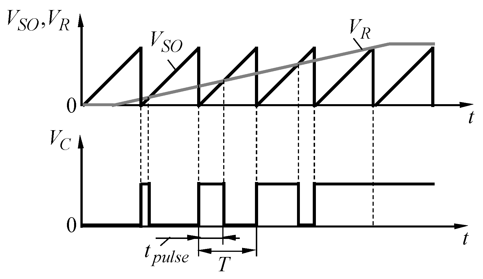
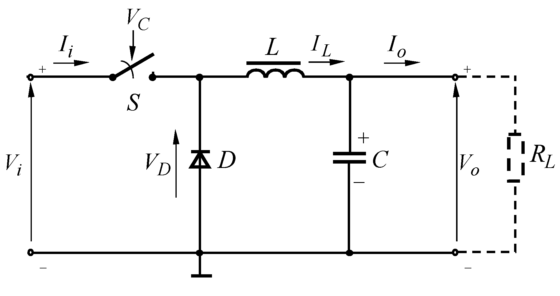
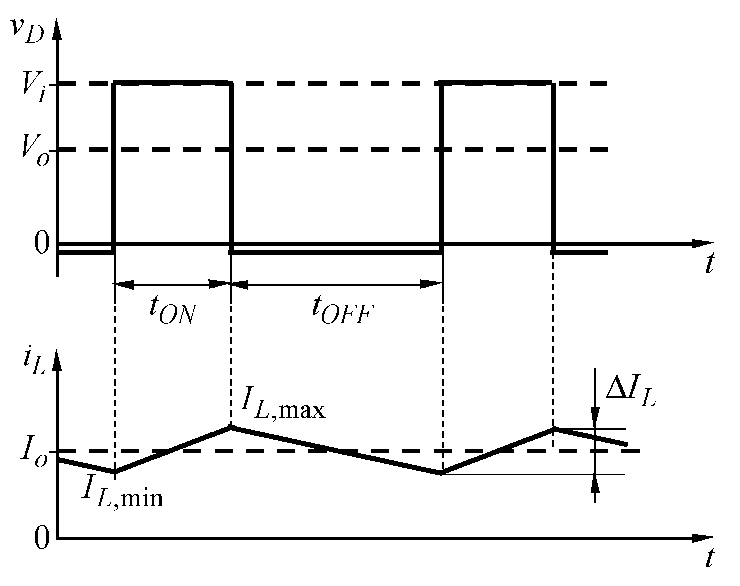
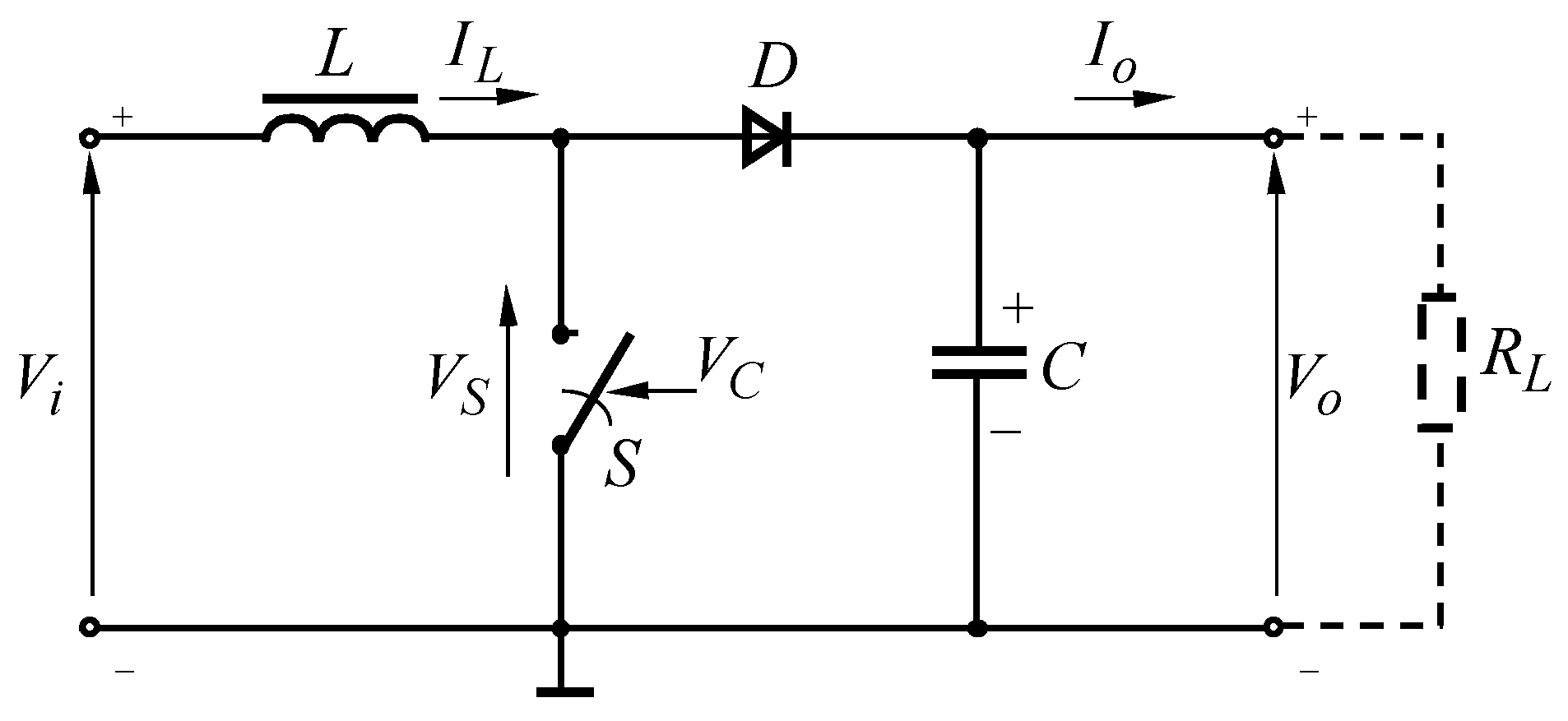

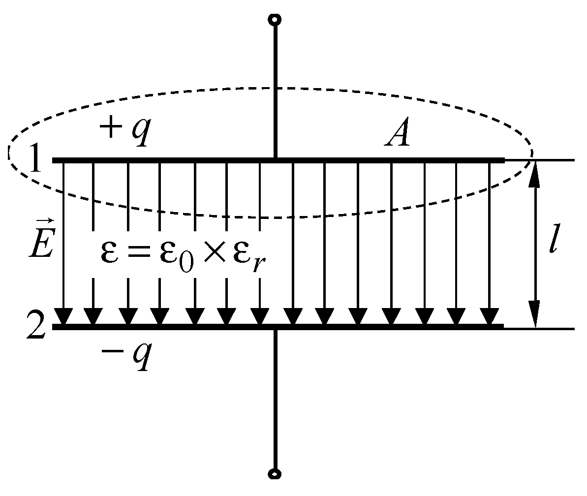


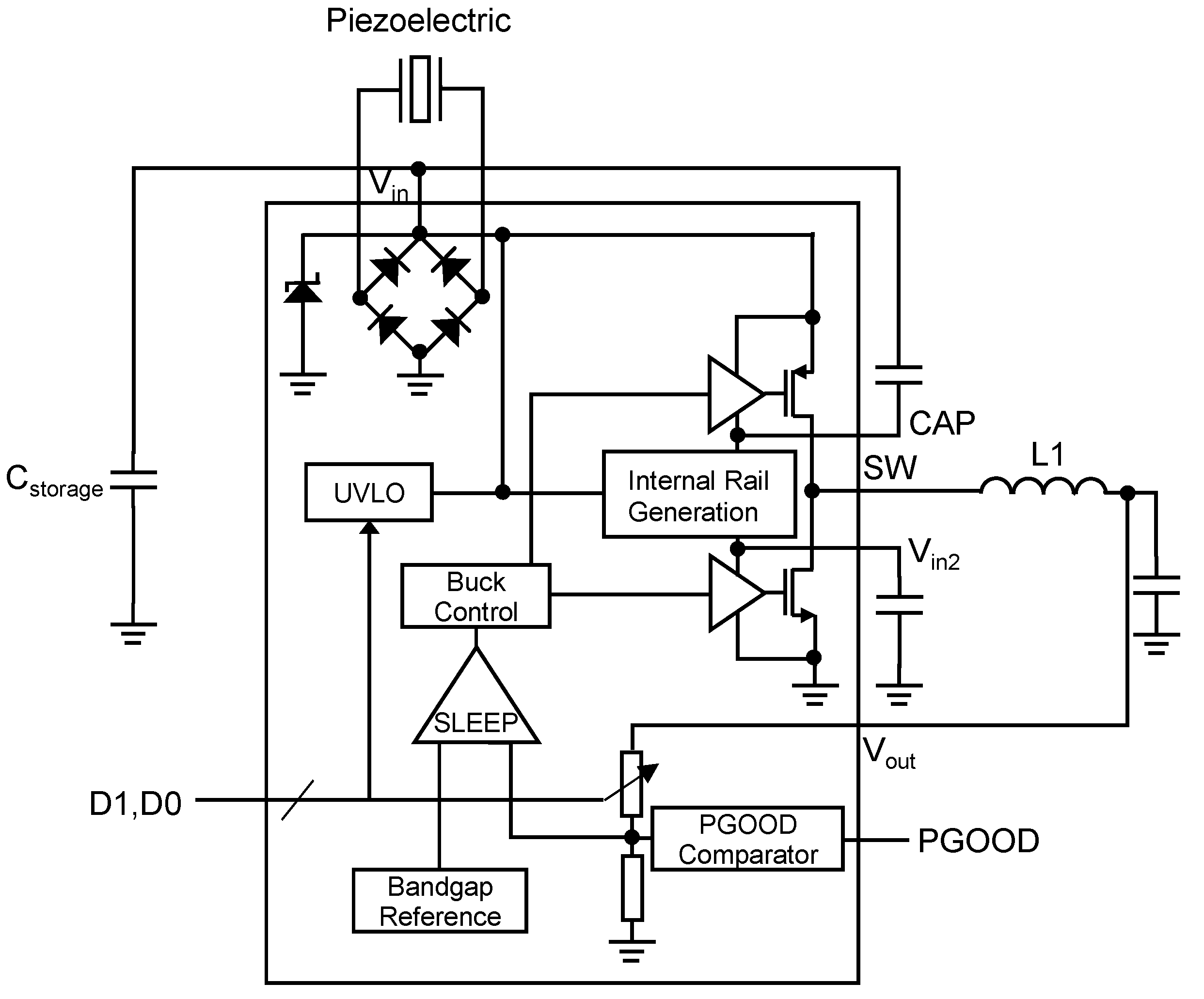

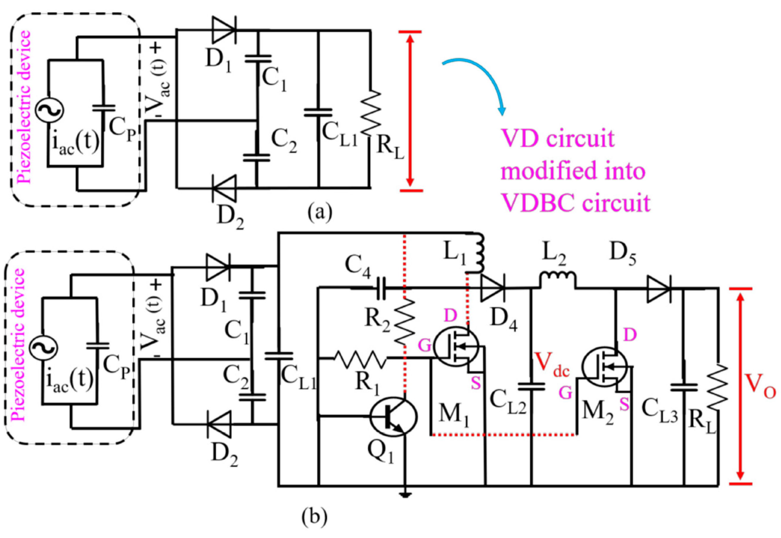

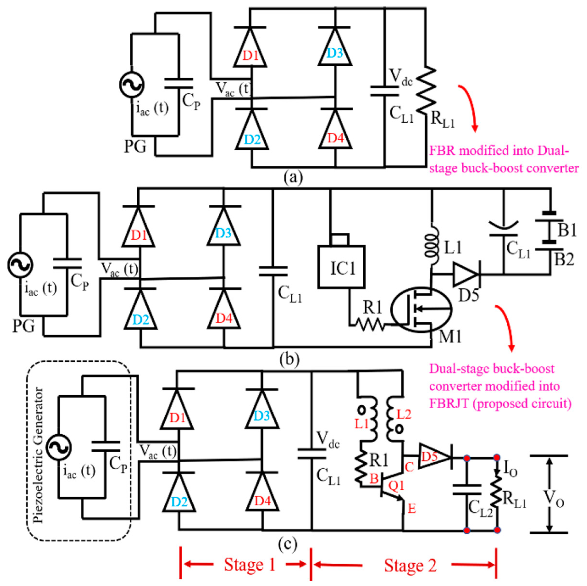
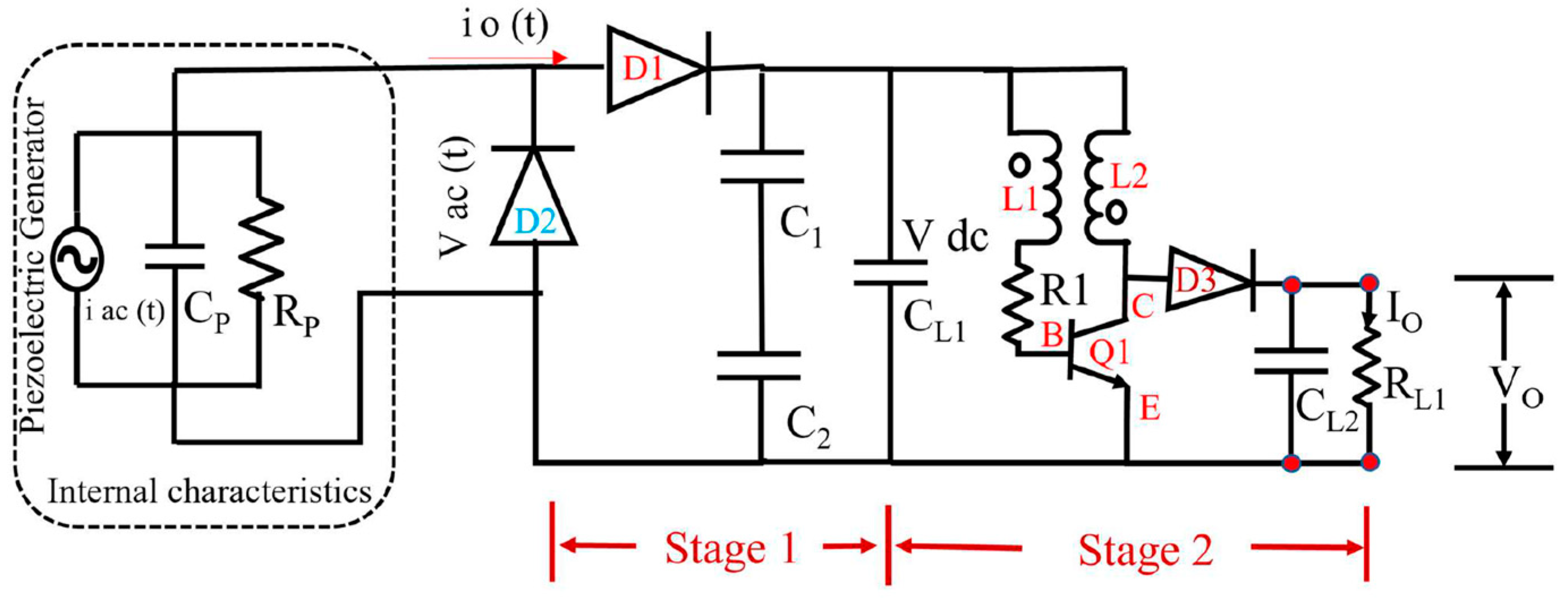
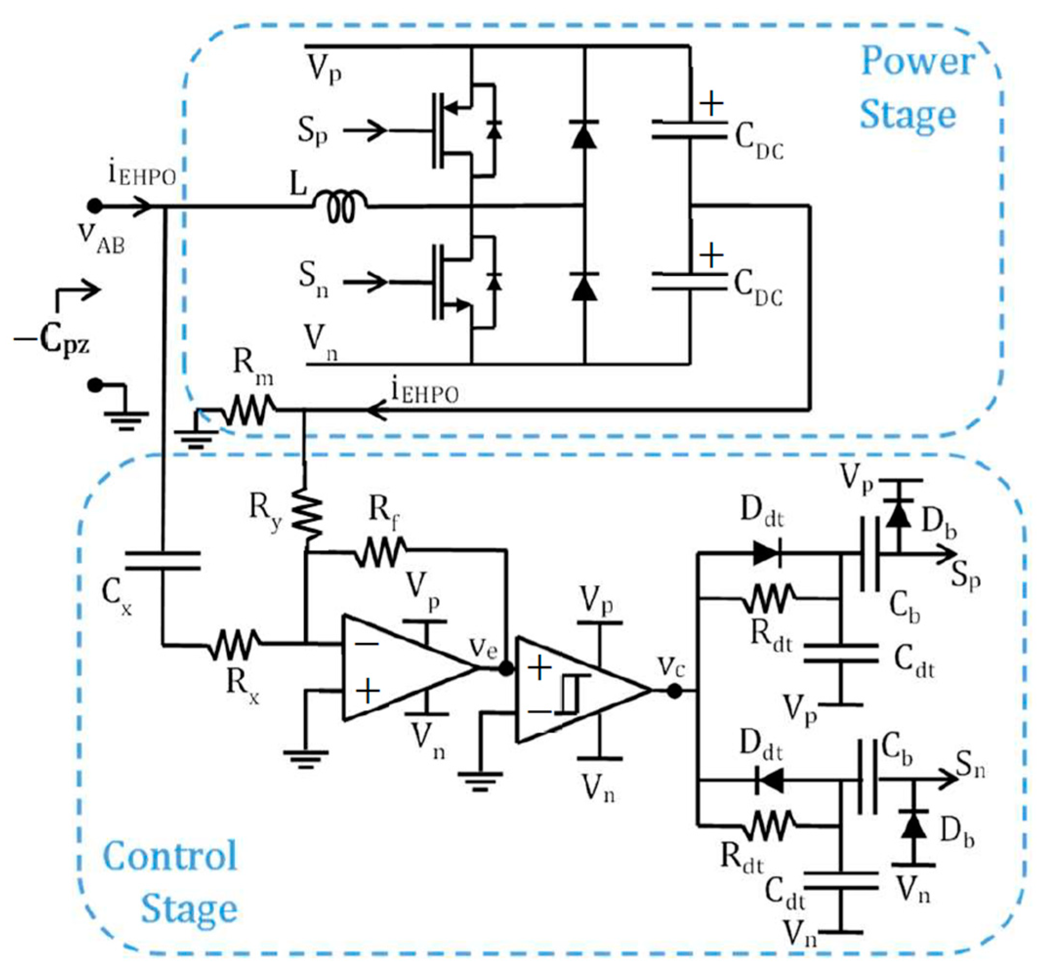
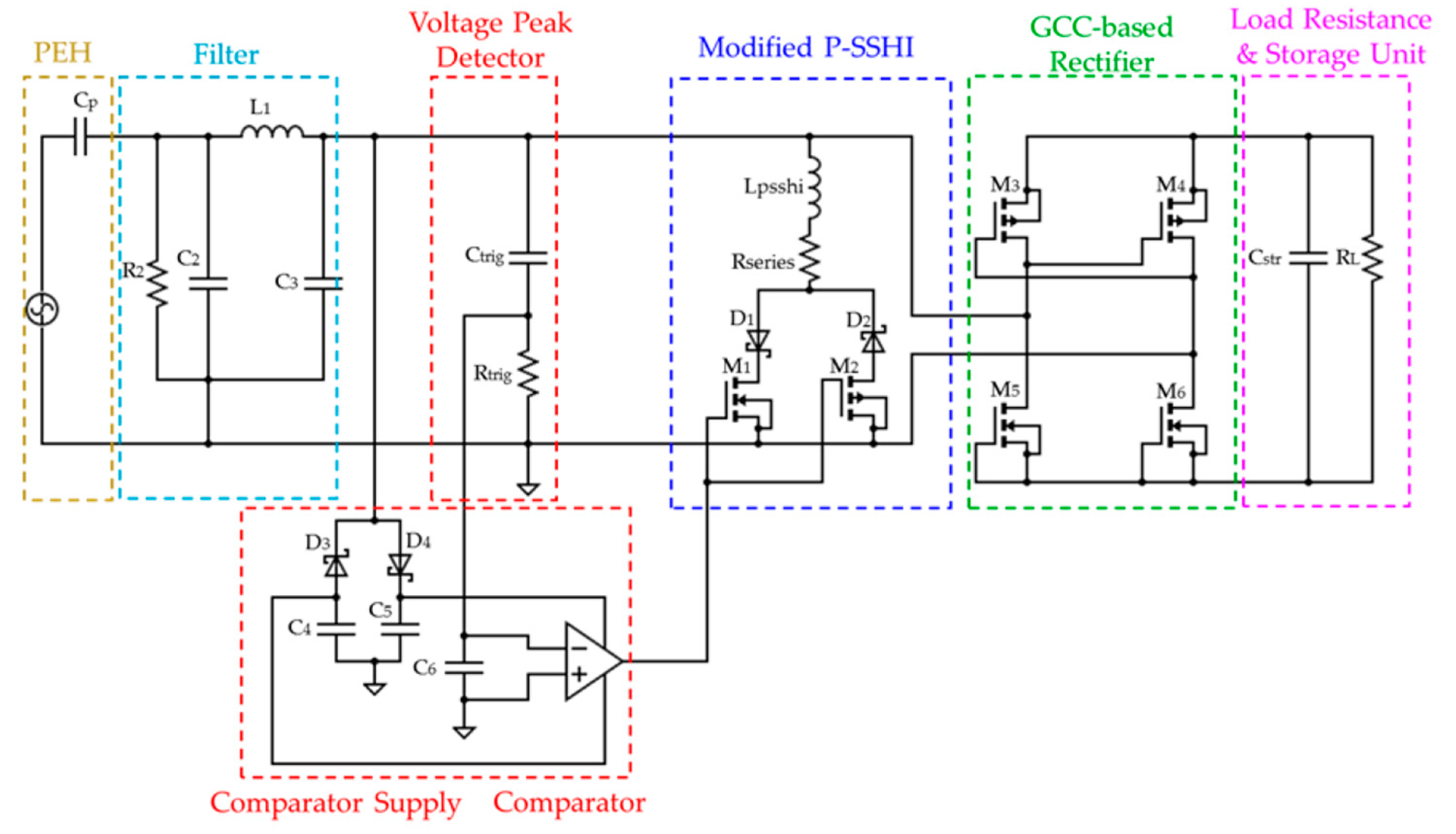
Disclaimer/Publisher’s Note: The statements, opinions and data contained in all publications are solely those of the individual author(s) and contributor(s) and not of MDPI and/or the editor(s). MDPI and/or the editor(s) disclaim responsibility for any injury to people or property resulting from any ideas, methods, instructions or products referred to in the content. |
© 2024 by the authors. Licensee MDPI, Basel, Switzerland. This article is an open access article distributed under the terms and conditions of the Creative Commons Attribution (CC BY) license (https://creativecommons.org/licenses/by/4.0/).